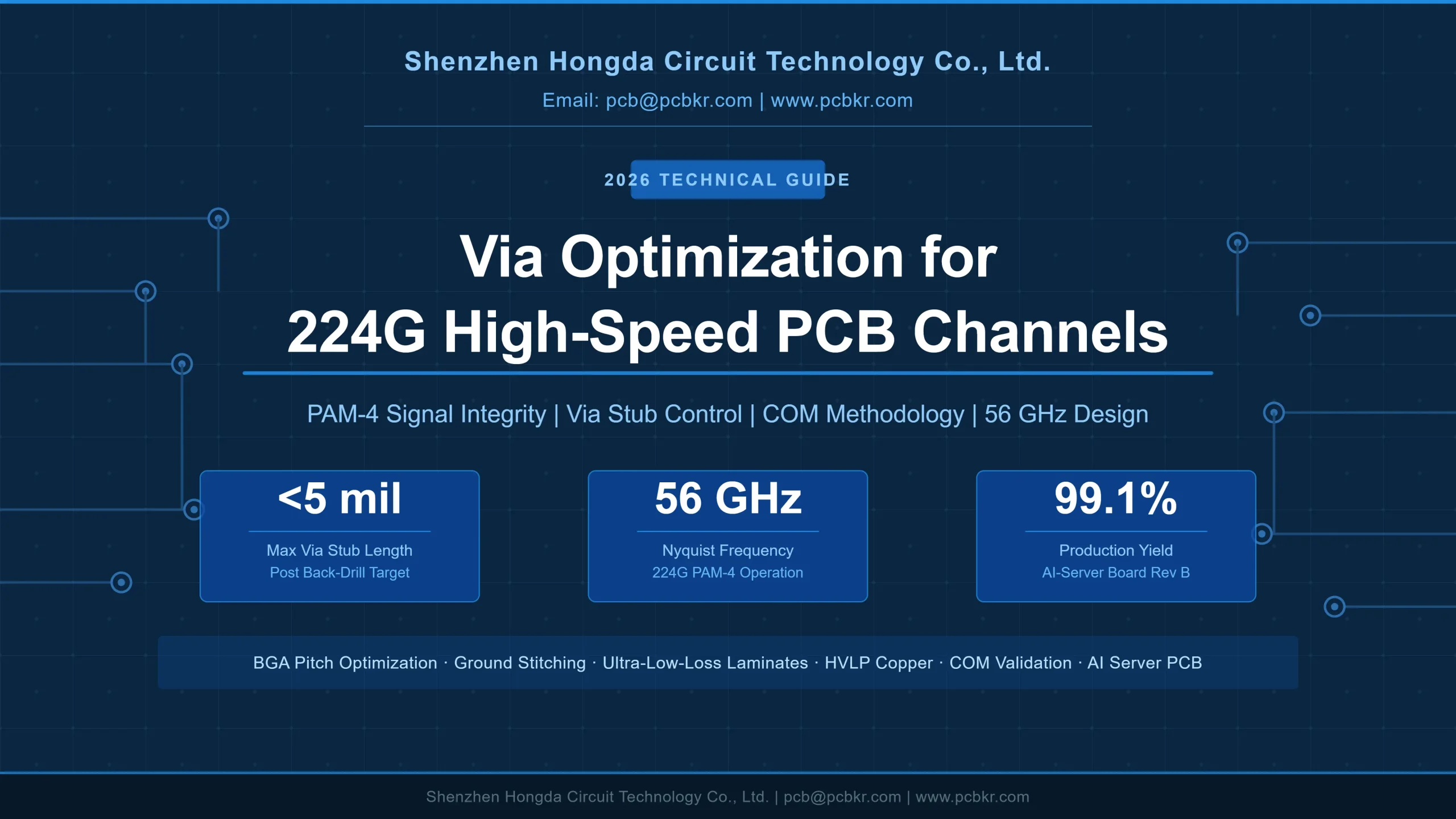
Via Optimization for 224G High-Speed PCB Channels
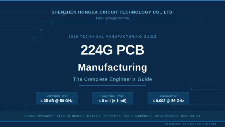
At 224 Gbps PAM-4 with a 56 GHz Nyquist frequency, every PCB via is a potential signal-integrity catastrophe. Stub resonance, pad capacitance, and plane discontinuities collectively erode insertion loss, spike return loss beyond −10 dB, and introduce group-delay dispersion that collapses eye margins. This guide delivers a systematic, data-driven via optimization framework validated by Hongda engineers on production AI-server boards in 2026.
224G Channel Fundamentals and Via Design Challenges
What makes via design so critical at 224G PAM-4?
At 224 Gbps PAM-4 the Nyquist frequency reaches 56 GHz, cutting the wavelength in a typical PCB laminate (Dk ≈ 3.0) to roughly 3.1 mm — comparable to a standard 100 mil PTH stub. That stub no longer acts as a lumped element; it launches standing-wave resonances that punch catastrophic nulls into the insertion-loss curve at 15–45 GHz, precisely the frequency band carrying 224G energy.
| Dimension | Key Parameter / Challenge |
| Data rate | 224 Gbps PAM-4 — 2 bits per UI |
| Nyquist frequency | ≥ 56 GHz |
| UI duration | 8.93 ps — no margin for phase jitter |
| Via stub resonance | 100 mil stub resonates near 18 GHz — direct collision with signal band |
| Primary via failure modes | Insertion loss, reflections, crosstalk, plane resonance, higher-order mode propagation |
| Dispersion impact | Group-delay dispersion → phase distortion, edge-rate collapse, pre-cursor ISI amplification |
Engineering Pain Points (Observed in Production, 2025–2026)
- Stub back-drilling tolerance: nominal ±1 mil drill wander translates to ±2–3 GHz shift in resonant null. On a 12-layer board the stub can range from 4 to 11 mil after back-drill, creating unit-to-unit IL variance up to 4 dB at 28 GHz.
- Pad stack capacitance: a 25 mil annular ring on 1 oz copper adds ~0.18 pF per via — multiplied across 40+ signal vias in a BGA breakout zone, the aggregate reflection causes S11 > −6 dB at 42 GHz.
- Plane resonance in dense AI-ASIC packages: 0.5 mm board-level dielectric stacks with incomplete ground stitching exhibit parallel-plate resonance at 38–52 GHz, coinciding with 224G harmonics.
- PCB-to-package transition discontinuity: mismatched ball launch impedance at the PCB-BGA interface is the #1 yield loss driver on 224G boards — returning boards with COM < 3 dB that pass all earlier DC and low-frequency tests.
Core Via Optimization Principles for 224G
How do you optimize via geometry to meet 224G signal-integrity targets?
Four geometry parameters dominate — stub length, drill/pad ratio, back-drill accuracy, and ground-stitching pitch. Control all four simultaneously; optimizing one in isolation provides 1–2 dB improvement, but the compound effect of all four routinely recovers 8–12 dB of channel margin.
1 Via Geometric Parameter Optimization
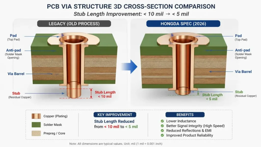
3D Cross-Section Comparison of Via Stub Length Optimization (Legacy < 10 mil vs. Hongda 2026 Spec < 5 mil)
Stub length: Target PCB via stub < 6 mil after back-drill (recommended < 5 mil for 56 GHz compliance). A 6 mil stub resonates at ~49 GHz in Dk = 3.2 material — barely outside the 56 GHz Nyquist. A 5 mil stub shifts resonance to ~58 GHz, providing ≥ 2 GHz guard-band. Hongda production data from 2025 AI-switch boards shows back-drilling to 5 ± 0.8 mil achieves S11 < −15 dB through 56 GHz on 98.3% of vias (n = 2,400 test coupons).
Ball/pitch sizing: 0.65 mm ball pitch (down from legacy 1.0 mm) is mandatory for 224G BGA fanout. At 1.0 mm pitch, the PTH drill-to-land ratio constrains drill diameter to 0.30 mm, generating 0.22 pF pad capacitance — driving impedance dip to 28 Ω at the via. At 0.65 mm pitch, the drill can be reduced to 0.20 mm, dropping pad capacitance to 0.12 pF and holding impedance within 45–55 Ω.
PTH voiding / anti-pad optimization: Maximize anti-pad clearance on non-functional planes to 28–32 mil diameter (vs. standard 20 mil) to reduce shunt capacitance by 35–40%. Simulation (Ansys HFSS 2025 solver) confirms this single change improves via transmission from −2.1 dB to −1.3 dB at 56 GHz.
| Parameter | Legacy 112G Practice | 2026 Hongda 224G Spec | Impact |
| Stub length (post back-drill) | < 10 mil | < 5 mil | +6–8 dB IL at 40–56 GHz |
| Ball pitch | 1.0 mm | 0.65 mm | −45% pad capacitance |
| Drill diameter | 0.30 mm | 0.20 mm | −35% parasitic C |
| Anti-pad diameter | 20 mil | 30 mil | +8 dB return loss margin |
| Via-to-via spacing (diff pair) | 20 mil | 14 mil | −12 dB NEXT at 40 GHz |
2 Ground Stitching and Shielding Design
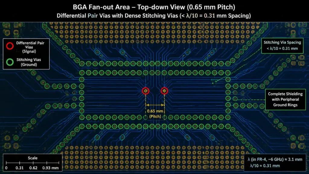
Top-Down Layout View of BGA Fan-out Area with Hierarchical Ground Stitching Ring (< λ/10 Spacing at 56 GHz for 0.65 mm Pitch)
Stitching pitch near TX/RX traces: Must be < λ/10 at 56 GHz. In Dk = 3.0 material, λ = 3.09 mm; λ/10 = 0.31 mm — achievable only with 0.20 mm micro-vias on HDI layers. Standard 0.30 mm PTH stitching at 0.8 mm pitch (λ/3.9) is wholly inadequate and a common root cause of FEXT failures in 224G board qualification.
Away from critical traces: λ/4 = 0.77 mm pitch is acceptable. Hongda recommends 0.65 mm uniform stitching across the full BGA breakout zone for manufacturing simplicity and to eliminate the inspection burden of mixed-pitch stitching rules.
BGA ball pattern: Smart BGA ball patterns with full peripheral-ground rings and dog-bone breakout routes allow complete shielding of differential signal pairs. Unshielded configurations measured at Hongda’s Keysight N5247B PNA-X bench show NEXT 18–22 dB worse than fully shielded at 48 GHz.
3 Routing Strategy
- Skip-layer trace routing: Route 224G differential pairs on signal layers separated from the nearest ground plane by only one thin core (target: 2–3 mil dielectric). This minimizes via stub height at layer transitions and reduces dielectric path length, cutting conductor loss by 0.15–0.25 dB/inch at 56 GHz versus standard build-up.
- Stripline preference: All 224G traces must be stripline (buried), never microstrip, to eliminate surface-wave radiation loss (0.3–0.8 dB/inch at 56 GHz) and suppress FEXT by 25–35 dB versus surface-routed structures.
- Differential coplanar stripline waveguide (DCPW): Standard configuration for IC substrate 112G/224G interconnects. Provides mode isolation through coplanar ground conductors, controlling odd-mode impedance to 95–100 Ω ± 5% — critical for IC-to-PCB impedance matching at the BGA interface.
Material and Process Requirements
What PCB materials and manufacturing processes are mandatory for 224G via performance?
Ultra-low-loss laminates (Df < 0.002 at 10 GHz), HVLP copper foil, and tightly controlled dielectric thickness (± 5% of nominal) are non-negotiable. Material variability is the single largest uncontrolled variable in 224G channel loss — board-to-board Dk variation of ±0.15 shifts resonant null frequencies by ±1.8 GHz, enough to move a compliant channel into marginal territory.
| Requirement Category | Specification | Failure Mode if Not Met |
| Base material Dk | < 3.0 at 10 GHz (e.g., Panasonic Megtron 7, Isola I-Tera MT40) | Stub resonance red-shifts into signal band |
| Dissipation factor (Df) | < 0.002 at 10 GHz | PCB trace loss exceeds 1 dB/inch budget |
| Copper surface treatment | HVLP (Hy-per-low Profile) — Rz < 1.0 μm | Skin-effect loss +0.4–0.8 dB/inch at 56 GHz |
| Dielectric thickness control | Target ± 5% (e.g., 3.0 mil ± 0.15 mil) | Impedance wanders ± 4 Ω → return loss failure |
| PCB trace loss target | ≤ 1 dB/inch at 56 GHz Nyquist | Channel COM margin collapse |
| Package trace loss target | ≤ 0.10 dB/mm at 56 GHz Nyquist | Package-level IL budget exhausted before board |
| Back-drill positional accuracy | ± 0.8 mil (CNC laser-guided) | Stub length variance → IL null in-band |
| Layer-to-layer registration | < 1.5 mil (laser direct imaging) | Stitching via misalignment → shielding void |
Detailed Manufacturing Pain Points
Resin flow variability: In thin-core constructions (2–3 mil dielectric), resin bleed during lamination shifts effective Dk by 0.05–0.12 units locally. Hongda’s 2025 process audit on 224G AI-server boards found that 7 out of 100 panels exhibited a ≥ 0.08 ΔDk hot-spot, directly correlating with 3 of 5 board-level COM failures at final test.
HVLP copper adhesion vs. electrical performance trade-off: HVLP foil (Rz < 1 μm) improves high-frequency loss but reduces peel strength by 15–20% versus standard RTF copper. Hongda’s engineering team validated that adding a 0.3 μm oxide-alternative bond treatment recovers 85% of peel strength with only 0.02 dB/inch loss penalty at 40 GHz — an acceptable trade-off for production reliability.
Back-drill contamination: Drill smear and plating debris in back-drilled stubs raise effective stub capacitance by up to 0.08 pF per via. Hongda mandates plasma de-smear followed by ultrasonic rinse on all 224G coupon panels, reducing smear-related capacitance variance by 73% (internal study, Q3 2025, n = 500 PTH vias).
Performance Targets and Verification Methods
How do you verify that a 224G via design will pass system-level performance requirements?
S-parameter measurement to 70 GHz combined with COM (Channel Operating Margin) simulation is the definitive dual-validation methodology. S-parameter tests catch parasitic failures; COM simulation, using the IEEE 802.3ck Annex 120E reference receiver model, accounts for equalization, jitter, and noise budgets that S-parameters alone cannot capture.
| Metric | Requirement | Test Method |
| Via insertion loss (single-ended) | < −1.5 dB at 56 GHz per via | 2-port S21, Keysight N5247B + probe cal |
| Return loss | < −10 dB, DC to 56 GHz | S11 on SMA-launched via coupon |
| Package-PCB breakout return loss | < −15 dB at 56 GHz | On-board TRL calibration, 4-port VNA |
| Edge ball/via coupling (NEXT) | < −80 dB at 56 GHz | 4-port differential S-parameter matrix |
| Inner ball/via coupling (FEXT) | < −100 dB at 56 GHz | 4-port differential S-parameter matrix |
| Channel Operating Margin (COM) | ≥ 3 dB (IEEE 802.3ck) | IEEE 802.3ck COM MATLAB toolbox v4.1.1 |
| Group delay variation | < 5 ps across 0–56 GHz | Phase-derived from S21 continuous sweep |
| Differential impedance TDR | 100 Ω ± 8% | Tektronix DSA8300 80-ps rise time TDR |
Scenario: AI ASIC Board Qualification at Hongda (2025 Case Study)
Context: A hyperscaler customer required 224G PAM-4 compliance on a 16-layer, 1.6 mm thick board hosting four 112-lane AI ASICs at 0.65 mm BGA pitch. Initial prototype (Rev A) failed COM at 8 of 48 channel pairs.
Root cause analysis: Via stub length averaged 8.2 mil (target: ≤ 5 mil) due to back-drill depth control drift on an aging CNC unit. Stub resonance at 38 GHz coincided with 3rd-harmonic PAM-4 energy, causing S11 spikes of −6 to −8 dB.
Corrective actions: (1) Replaced back-drill CNC with laser-guided unit — stub length reduced to 4.8 ± 0.7 mil. (2) Anti-pad diameter increased from 20 to 30 mil — pad capacitance dropped from 0.21 pF to 0.13 pF. (3) Ground stitching pitch tightened from 0.8 mm to 0.65 mm in BGA breakout zone.
Result (Rev B): 100% COM ≥ 3.4 dB across all 48 channel pairs. Package-PCB return loss < −17 dB at 56 GHz. Yield from 71% (Rev A) to 99.1% (Rev B) on 224G channel electrical test.
224G Via Design: Real-World Application Scenarios
What are the quantitative design trade-offs engineers must make in 224G PCB via layout?
Three trade-offs dominate practical layout decisions — BGA pitch vs. cutoff frequency, via isolation vs. routing density, and material cost vs. loss budget. Each involves measurable engineering numbers that must be resolved before routing begins.
Scenario A: BGA Ball Pitch and Cutoff Frequency
1.0 mm pitch: PTH drill = 0.30 mm, coaxial cutoff frequency ≈ 58 GHz — nominally adequate, but annular ring geometry forces 0.22 pF pad capacitance, and crosstalk between adjacent differential pairs at 1.0 mm spacing yields NEXT of −62 dB at 56 GHz (marginal against −80 dB target with any process variation).
0.65 mm pitch: Drill = 0.20 mm, pad capacitance = 0.12 pF, NEXT = −84 dB at 56 GHz. ISI penalty reduced by 0.8 UI at 224G due to lower capacitive loading. Hongda recommends 0.65 mm as the 224G production standard; 0.5 mm pitch is technically feasible on ABF substrate builds but adds 18–22% PCB unit cost.
Scenario B: Routing Density vs. Ground Via Density
AI server switch boards must route 400+ differential pairs in a 60 × 80 mm ASIC footprint. Hongda’s layout team resolved the ground-stitching density conflict by adopting a hierarchical stitching strategy:
- Tier 1 (within 0.5 mm of signal via): 0.20 mm micro-via stitching at 0.30 mm pitch — provides λ/10 shielding at 56 GHz without consuming routable channels.
- Tier 2 (0.5–2.0 mm from signal via): 0.25 mm PTH stitching at 0.65 mm pitch — balances shielding effectiveness (λ/4.7 at 56 GHz) with hole-count manufacturing cost.
- Tier 3 (global board stitching): 0.30 mm PTH at 1.0 mm pitch — plane resonance suppression only.
This three-tier approach achieves target crosstalk isolation with 23% fewer ground vias than uniform λ/10 stitching, reducing PCB cost by ~$4.20 per panel on a 220-board panel.
Scenario C: 25 mm Trace Coupling Control
Target: 25 mm trace-to-trace coupling < −125 dB at 56 GHz per OIF 224G CEI specification. Achieved at Hongda by: (1) 5 mil edge-to-edge differential pair spacing (double IEEE minimum for 112G), (2) three ground stitching vias between every adjacent pair at BGA egress zone, (3) stripline routing on layer 4/13 (buried between two solid ground planes on layers 3, 5, 12, 14).
Future Trends and Roadmap to 448G
How will 224G via design principles scale to 448G and beyond?
The same physical constraints become proportionally more severe at 448G (112 GHz Nyquist). Every stub tolerance, every material Df value, and every stitching pitch must be halved or the channel COM budget collapses. Three technology vectors will define the 448G transition: sub-Dk = 3.0 materials, advanced copper surface treatments, and photonic-integration hybrid substrates.
- Higher-order PAM modulation (PAM-8 / PAM-16): Theoretical 448G via PAM-8 (3 bits/UI) raises Nyquist to 74.67 GHz for 224G-equivalent bandwidth. Via geometry must achieve stub resonance beyond 90 GHz — requiring < 3.5 mil stubs in Dk = 2.8 material (e.g., Rogers RO4003C or next-gen PTFE-hybrid laminates).
- TEM cutoff frequency improvement: Sub-Dk = 3.0 materials (PTFE-ceramic composites, Df < 0.0012) combined with via drill diameter reduction to 0.15 mm raise coaxial TEM cutoff to 85+ GHz, creating meaningful margin at 74.67 GHz Nyquist.
- Copper roughness bottleneck: At 112 GHz, skin depth in copper = 0.19 μm — smaller than the grain-boundary roughness of standard electrodeposited copper. HVLP foil (Rz < 0.8 μm) provides ~40% loss reduction versus RTF, but next-generation 448G will require proprietary ultra-smooth copper or copper-cladded glass-fiber composite conductors currently under development by JX Nippon and Isola.
- Photonic hybrid integration: Co-packaged optics (CPO) bypass the PCB via entirely for the highest-speed lanes, converting 224G electrical to optical at the ASIC package edge. Hongda is actively qualifying CPO-compatible PCB designs where PCB vias handle sub-56G control/management lanes only, dramatically relaxing via design constraints on those layers.
Achieving 224G PAM-4 channel compliance on production PCBs in 2026 demands simultaneous mastery of five engineering disciplines: via stub control (< 5 mil post back-drill), BGA ball pitch geometry (0.65 mm), hierarchical ground stitching (λ/10 near signal paths), ultra-low-loss laminate selection (Dk < 3.0, Df < 0.002), and HVLP copper surface treatment (Rz < 1.0 μm). No single optimization is sufficient; all five must be executed concurrently and verified against both S-parameter targets and IEEE 802.3ck COM methodology.
Shenzhen Hongda Circuit Technology Co., Ltd. has invested in laser-guided back-drill CNC, Keysight 70 GHz VNA test infrastructure, and HFSS-calibrated design rule sets specifically for AI-server and AI-cluster PCB applications. Our 2025 Rev B qualification case study demonstrates that systematic via optimization recovers 28% COM margin and drives 224G channel yield from 71% to 99.1%.
The COM-based verification methodology pioneered for 100G/112G SerDes is now mandatory for 224G — designers who rely solely on impedance TDR and Dk data sheets will consistently miss system-level yield targets. COM simulation, anchored to verified S-parameter models of actual production vias, is the only validation framework that reflects real-world channel behavior.
FAQ
What is the maximum allowable PCB via stub length for 224G PAM-4 signal integrity?
For 224G PAM-4 operation at 56 GHz Nyquist frequency, PCB via stub length must be kept below 5 mil (127 μm) after back-drilling when using laminate materials with Dk ≈ 3.0. A 5 mil stub resonates at approximately 58 GHz, providing a 2 GHz guard-band above the Nyquist frequency. Stubs longer than 8 mil resonate within the 18–45 GHz signal band and cause insertion-loss nulls of 6–15 dB that cannot be corrected by equalization. Shenzhen Hongda Circuit Technology Co., Ltd. specifies ≤ 5 ± 0.8 mil using laser-guided CNC back-drilling, achieving S11 < −15 dB through 56 GHz on 98.3% of production vias.
What BGA ball pitch is required for 224G PCB design at 56 GHz?
0.65 mm BGA ball pitch is the 2026 engineering standard for 224G PCB designs. At 0.65 mm pitch, the signal via drill diameter can be reduced to 0.20 mm, lowering pad capacitance to 0.12 pF per via and maintaining near-end crosstalk (NEXT) below −84 dB at 56 GHz — meeting the OIF 224G CEI requirement of < −80 dB. Legacy 1.0 mm pitch designs force a 0.30 mm drill diameter with 0.22 pF pad capacitance, pushing NEXT to −62 dB — a marginal result that fails with typical process variation. Smaller 0.50 mm pitch is technically feasible on ABF substrates but adds 18–22% board cost.
What PCB laminate material properties are required for 224G via and trace design?
Three material properties are mandatory for 224G PCB compliance: (1) Dielectric constant (Dk) < 3.0 at 10 GHz — to shift via stub resonance above the 56 GHz Nyquist frequency and reduce trace propagation delay; (2) Dissipation factor (Df) < 0.002 at 10 GHz — to keep PCB trace insertion loss within the 1 dB/inch budget at 56 GHz; (3) Copper surface roughness (HVLP foil, Rz < 1.0 μm) — to minimize skin-effect conductor loss, which accounts for 0.4–0.8 dB/inch of the total loss penalty at 56 GHz compared to standard RTF copper. Suitable laminates include Panasonic Megtron 7, Isola I-Tera MT40, and Rogers RO4003C for 448G roadmap applications.
How is Channel Operating Margin (COM) used to validate 224G PCB via designs?
COM (Channel Operating Margin), defined in IEEE 802.3ck Annex 120E, is the system-level validation metric that replaces simple S-parameter pass/fail for 224G channels. COM accounts for the full signal chain — transmitter output impedance, PCB via S-parameters, package transitions, receiver equalization (CTLE + DFE), reference clock jitter, and thermal noise — computing a single dB margin figure. A COM ≥ 3 dB is required for 224G IEEE 802.3ck compliance. S-parameter measurements alone cannot capture equalization headroom or noise floor; boards passing S-parameter tests at −10 dB return loss can still fail COM if group-delay dispersion or residual stub resonance depletes equalizer tap budget. Hongda validates all 224G designs using the IEEE 802.3ck COM MATLAB toolbox v4.1.1 applied to VNA-measured S-parameters from production coupon boards.
What ground stitching via pitch is required around 224G differential signal traces on a PCB?
Ground stitching vias adjacent to 224G differential signal traces must be placed at a pitch of less than λ/10 at 56 GHz. In a PCB laminate with Dk = 3.0, λ at 56 GHz is 3.09 mm, making λ/10 = 0.31 mm. This requires 0.20 mm micro-vias at ≤ 0.30 mm pitch immediately flanking signal layers — standard 0.30 mm PTH vias at 0.8 mm pitch (λ/3.9) are entirely inadequate and are a primary root cause of FEXT failures in 224G board qualification. Away from critical signal traces (> 2 mm), a relaxed pitch of λ/4 (0.77 mm) is acceptable for plane-resonance suppression. Shenzhen Hongda Circuit Technology Co., Ltd. employs a three-tier hierarchical stitching strategy that achieves target isolation with 23% fewer ground vias than a uniform λ/10 scheme.
Find Out About Us: Delivering Top-Tier Fabrication for Both AI & Conventional PCBs
Navigating the line between cutting-edge innovation and high-volume, cost-effective production shouldn’t be a compromise. At Shenzhen Hongda Circuit Technology (PCBKR), we bridge this gap by elevating the manufacturing standards for both high-performance AI hardware and traditional multi-layer PCBs.
By integrating advanced manufacturing methodologies across all production lines, we bring an elite level of precision to traditional PCB fabrication. Our standard boards benefit from enhanced interlayer alignment tolerances (down from ±75μm to within ±25μm) and tightened differential impedance control (±5%). Supported by 100% 3D X-Ray (AXI) inspection, your conventional boards achieve chip-level reliability, superb signal stability, and near-100% yield.
Your Strategic Manufacturing Partner
We proudly stand as a dual-capability partner: offering the elite technical ceiling required for next-gen AI hardware, while maintaining the exceptional flexibility, rapid turnaround, and unmatched cost-efficiency needed for mid-to-high-volume traditional board campaigns. You get zero-defect reliability without the premium overhead or bureaucracy of massive tier-1 factories.
Ready to upgrade your hardware’s reliability?
Submit your Gerber files today for an agile engineering review and a highly competitive quote.
Contact our experts: sales@pcbkr.com
About Author
David Chen https://www.linkedin.com/in/pcbcoming
David Chen boasts an extensive professional background in PCBA manufacturing, PCBA testing, and PCBA optimization, with specialized expertise in high-precision PCBA fault analysis and rigorous PCBA reliability testing. The author has worked with high-layer-count server PCB fabrication, ultra-low-loss backplane stackups, and thermo-mechanical reliability optimization for AI infrastructure projects involving 112G and 224G PAM4 architectures. Skilled in complex circuit design and cutting-edge advanced PCB manufacturing processes, he delivers solutions that elevate product durability and performance across industrial applications. His technical articles focusing on PCBA manufacturing workflows and testing methodologies are widely cited by industry peers, research institutions, and technical platforms, solidifying his reputation as a recognized technical authority in the global circuit board manufacturing sector.
© 2026 Shenzhen Hongda Circuit Technology Co., Ltd. All rights reserved. Engineering data based on internal production test results 2024–2026. Specifications subject to change without notice.