Laser Microvia Drilling Technology and Capabilities: UV, CO₂, and Femtosecond Systems for Precision HDI PCB Fabrication
Introduction: The Laser as the Defining Tool of Modern HDI Manufacturing
In the hierarchy of PCB manufacturing capabilities, laser microvia drilling sits at the intersection of physics, precision engineering, and production economics. No other single process step has as much impact on the density, reliability, and electrical performance of a high-density interconnect (HDI) board. And no other process step is as poorly understood by procurement teams evaluating suppliers.
If you are sourcing High-Density Interconnect (HDI) Microvia PCB Manufacturing | mSAP & SAP Capabilities for AI Server and HPC Applications for an AI server backplane, an 800G optical module, or a smartphone motherboard, you need to look beyond the supplier’s claim of “laser drilling available The critical questions are: What wavelength? What pulse duration? What positional accuracy? What aspect ratio? What desmear process? And most importantly—what is the actual yield on stacked microvia structures under thermal cycling?
This article provides a comprehensive technical and procurement-oriented analysis of PCB microvia drilling technology as it exists in 2026. We will examine UV, CO₂, and femtosecond laser systems; compare stacked versus staggered microvia architectures; analyze aspect ratio limits and reliability implications; and provide a qualification framework for verifying that a supplier’s laser drilling capability matches their marketing claims.
At Shenzhen Hongda Circuit Technology Co., Ltd. , our laser drilling infrastructure includes Mitsubishi UV/CO₂ hybrid systems, femtosecond laser platforms for advanced interposer applications, and automated optical registration with real-time beam profiling, paired with precision fine-line production via mSAP Process in Microvia PCB Fabrication: Why Modified Semi-Additive Technology Is the Only Path to Sub-15μm Routing for AI Chip Carriers. Our production floor drills approximately 2.5 million microvias per day across HDI, rigid-flex, and substrate-like PCB (SLP) builds. The specifications and process data in this article reflect our actual production parameters.
The Physics of Microvia Formation: How Lasers Create Interconnects
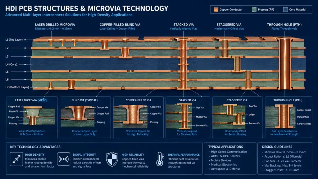
HDI PCB Structures & Microvia Technology Cross-Section
Ablation Mechanisms: Photochemical vs. Photothermal Decomposition
Laser drilling of microvias operates on two distinct physical principles, depending on wavelength and pulse duration:
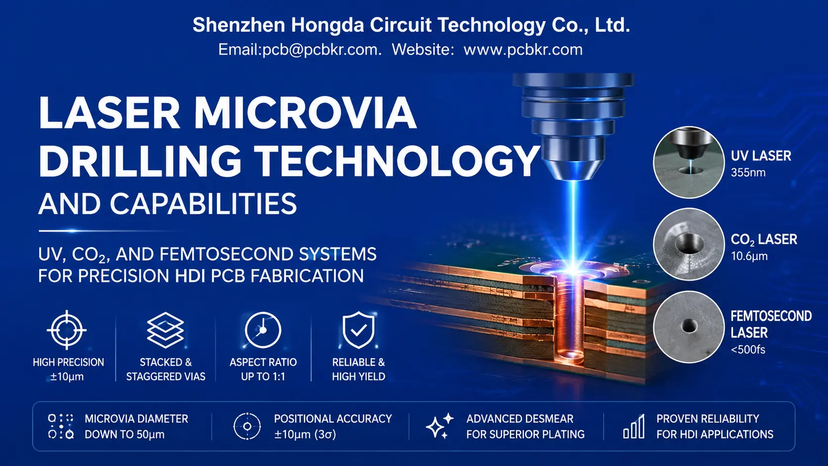
Photothermal Ablation (CO₂ Lasers) CO₂ lasers operate at 9.3–10.6 μm wavelength, where photon energy is absorbed by the molecular bonds of organic dielectrics (epoxy resins, polyimides, build-up films). The absorption is strong and localized, causing rapid thermal decomposition—essentially vaporizing the material. The process is efficient for dielectric removal but produces a characteristic tapered hole profile due to the Gaussian intensity distribution of the beam. This taper is actually beneficial for subsequent plating, as it improves copper throw into the via barrel. However, excessive taper can reduce the effective landing pad diameter and create resin smear at the via bottom.
Photochemical Ablation (UV Lasers) UV lasers—typically 355 nm frequency-tripled Nd:YAG (DPSS) sources—operate at photon energies that exceed the work function of copper. This enables cold ablation: the laser breaks molecular bonds through photochemical decomposition rather than thermal heating. The result is cleaner sidewalls, smaller heat-affected zones (HAZ), and the ability to drill through both copper foil and dielectric in a single process step. UV lasers are essential for stacked microvia structures where thermal damage to underlying layers must be minimized.
Ultrafast Ablation (Femtosecond/Picosecond Lasers) Femtosecond lasers (pulse duration <1 ps) operate in a regime where the pulse is shorter than the thermal diffusion time of the material. Energy is deposited so rapidly that it vaporizes material before heat can conduct to surrounding regions. This produces virtually zero heat-affected zone, enabling microvia diameters below 50 μm in temperature-sensitive materials like high-Tg polyimides. At Hongda Circuit, we have qualified femtosecond sources for 20–30 μm microvias in rigid-flex and SLP applications where standard UV/CO₂ systems reach their limit.
Why Mechanical Drilling Cannot Compete for Microvias
Mechanical drill bits, even carbide micro-drills, face fundamental limitations, you can compare all pros and cons in our complete Microvia vs. Through-Hole PCB: Key Differences and Selection Guide.
• Minimum practical diameter: 150–200 μm due to bit deflection, runout, and breakage
• Aspect ratio limit: 8:1 for reliable plating; 10:1 at the absolute extreme
• Positional accuracy: ±25 μm under ideal conditions, degrading with bit wear
• Surface damage: Mechanical stress can delaminate thin build-up dielectrics
• Tooling cost: Micro-drills below 0.3 mm require frequent replacement, increasing cost per hole
For comparison, our laser systems achieve 50 μm diameters routinely, 20 μm in advanced qualification, with positional accuracy of ±5 μm and no mechanical contact with the board surface. The economic crossover point—where laser drilling becomes cheaper than mechanical drilling—occurs at approximately 0.25 mm hole diameter. For microvias, there is no contest.
Laser System Technologies: UV, CO₂, and Hybrid Configurations
UV DPSS Laser Drilling: Precision for Stacked Microvia Structures
Our Mitsubishi UV DPSS (Diode-Pumped Solid-State) laser drilling systems represent the current production standard for high-reliability HDI microvias. Key specifications:
| Parameter | Specification | Significance |
|---|---|---|
| Wavelength | 355 nm | Penetrates copper and dielectric; cold ablation |
| Pulse Duration | ~20 ns | Balances ablation efficiency and HAZ control |
| Beam Quality (M²) | <1.3 | Tight focus spot for small diameters |
| Positional Accuracy | ±5 μm (3σ) | Ensures alignment to BGA pads and inner layer targets |
| Repeatability | ±3 μm | Critical for stacked via alignment |
| Minimum Via Diameter | 50 μm (production); 75 μm (standard) | Supports 0.3 mm pitch BGA escape |
| Maximum Drilling Rate | 1,200 holes/second | High throughput for dense panels |
| Depth Control | ±8 μm | Prevents over-drilling into inner layers |
The UV laser process sequence at Hongda Circuit is:
- Panel alignment: Four-edge fiducial recognition with sub-pixel interpolation
- Copper opening: Low-fluence UV pulses ablate the top copper foil (8–12 μm) to expose dielectric
- Dielectric ablation: Higher-fluence pulses remove epoxy/build-up material to the capture pad
- Quality verification: Inline vision system checks hole diameter, position, and bottom cleanliness
- Panel indexing: Automatic panel advance for next drilling field
UV lasers excel in applications requiring stacked microvia structures, where multiple blind vias are aligned vertically. The minimal HAZ prevents thermal damage to the copper pad of the underlying via, preserving plating adhesion at the stack interface.
CO₂ Laser Drilling: Throughput for Standard Blind Vias
Our CO₂ laser systems are optimized for high-volume production of standard blind microvias in build-up layers. Key specifications:
| Parameter | Specification | Significance |
|---|---|---|
| Wavelength | 9.3 μm (tuned for epoxy absorption) | Maximizes ablation efficiency; minimizes collateral heating |
| Pulse Duration | ~100 μs | Thermal decomposition regime for clean dielectric removal |
| Positional Accuracy | ±8 μm | Adequate for standard HDI and consumer electronics |
| Minimum Via Diameter | 75 μm (production); 100 μm (standard) | Cost-effective for non-stacked applications |
| Maximum Drilling Rate | 2,500 holes/second | Highest throughput for dense panels |
| Natural Copper Stop | Yes | CO₂ wavelength reflects from copper, self-limiting drill depth |
CO₂ lasers have a natural advantage: the 9.3 μm wavelength is strongly absorbed by epoxy dielectrics but reflected by copper. This means the laser automatically stops when it reaches the copper capture pad, making depth control inherently simpler than UV systems. However, CO₂ lasers cannot drill through copper—they require a pre-etched opening or a UV “pilot” pulse to expose the dielectric.
At Hongda Circuit, we use CO₂ lasers for: – Standard blind vias in consumer electronics and automotive HDI – High-volume builds where throughput outweighs the need for minimum diameter – Build-up layer drilling where natural copper stop simplifies process control
Hybrid UV/CO₂ Systems: The Best of Both Worlds
The latest 2026 laser drilling platforms combine both technologies in a single integrated system. The UV laser performs copper opening and precision dielectric ablation for small-diameter vias, while the CO₂ laser handles bulk dielectric removal for larger vias or high-density arrays. This hybrid approach:
• Reduces cycle time by 30–40% compared to pure UV drilling
• Maintains precision for critical stacked via structures
• Optimizes cost per hole by using the most efficient laser for each task
• Improves yield by matching laser type to via specification
Our 2026-capacity expansion includes two additional hybrid systems to support the surge in AI server and optical module demand.
Femtosecond Laser Drilling: The Frontier of Ultra-Fine Microvias
For applications pushing beyond standard HDI—rigid-flex wearables, advanced interposers, and CoWoP substrate-like PCBs—we have qualified femtosecond laser sources that achieve:
• 20–30 μm microvia diameters in 25 μm build-up dielectrics
• <5 μm heat-affected zone in high-Tg polyimide flex layers
• ±3 μm positional accuracy for interposer alignment features
• Clean sidewalls with no resin smear, eliminating desmear variability
Femtosecond systems are not yet cost-competitive for high-volume production, but they are indispensable for prototype builds and low-volume, high-mix applications where standard lasers cannot meet geometric requirements.
Microvia Architecture: Stacked vs. Staggered vs. Skip-Via
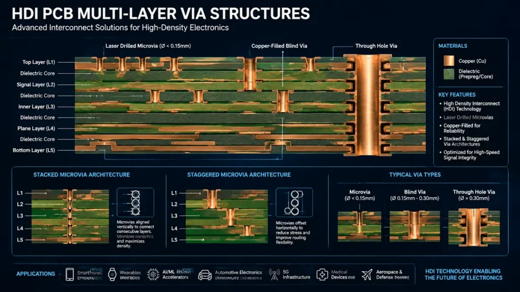
HDI PCB Multi-Layer Via Structures & Technologies
Stacked Microvias: Maximum Density, Managed Risk
Stacked microvias are multiple blind vias aligned vertically, creating a direct copper column through multiple build-up layers. They are essential for Any-Layer HDI and ultra-dense BGA escape routing, but they concentrate mechanical and thermal stress.
Procurement Risk Factors for Stacked Microvias:
- Thermal cycling vulnerability: Vertical alignment creates a continuous stress path. CTE mismatch between copper and epoxy generates shear stress at every layer interface. Under thermal shock (–65°C to +150°C), stacked vias can fail through barrel cracking or pad lift at 300–500 cycles if not properly designed.
- Plating quality sensitivity: The bottom of a stacked via is the top of the via below it. If the lower via has plating voids or incomplete copper fill, the upper via’s reliability is compromised from the start.
- Alignment tolerance accumulation: In a 4-high stack, a ±5 μm misalignment per layer can accumulate to ±20 μm at the top—enough to miss a 75 μm BGA pad entirely.
PHongda Circuit’s Stacked Microvia Protocol: – Maximum stack height: 3 vias for standard builds; 4 vias only with copper-filled and planarized structures – Copper fill requirement: All buried vias in the stack must be void-free copper filled – Alignment verification: 100% automated optical inspection (AOI) of stack registration before lamination – Reliability validation: IST (Interconnect Stress Test) and 1,000-cycle thermal shock on every new stackup design
Staggered Microvias: Distributed Stress, Proven Reliability
Staggered microvias offset each blind via from the one above and below it, distributing thermal and mechanical stress across a wider area. They require slightly more routing area than stacked vias but offer significantly higher reliability.
When to Specify Staggered Microvias: – Automotive ADAS modules subject to under-hood thermal cycling and vibration – Aerospace and defense applications requiring MIL-STD-883 qualification – Medical implants where failure is not an option – Any design where the layout density permits the additional space
Our production data shows that staggered microvias in 2+2+2 structures with aspect ratios below 0.75:1 routinely pass 1,000+ thermal cycles without resistance shift exceeding 10%. This is why we recommend staggered configurations as the default for reliability-critical applications, reserving stacked vias only for density-constrained areas.
Skip-Vias: The Efficiency Play
Skip vias (also called skip-layer vias) connect non-adjacent layers—e.g., L1 directly to L3, bypassing L2. They reduce the number of microvias needed for a given interconnection, lowering manufacturing cost and improving reliability by eliminating unnecessary layer transitions.
Design Rule: Skip vias should be used whenever the electrical design permits. They are particularly valuable in server motherboard PCB designs where power rails need to penetrate multiple layers without consuming routing resources on intermediate layers.
| Parameter | Stacked Microvia | Staggered Microvia | Skip-Via |
|---|---|---|---|
| Routing Density | Highest | High | Medium |
| Reliability (Thermal Cycles) | 300–500 (moderate) | 1,000+ (excellent) | 800+ (very good) |
| Manufacturing Complexity | High (requires fill + planarization) | Medium | Low |
| Cost Impact | +25–40% vs. staggered | Baseline | –15% vs. staggered |
| Best Application | Any-Layer HDI, smartphone SLP | Automotive, aerospace, medical | Server motherboards, power distribution |
| IPC-2226 Guideline | Max 2 stacked; 3 with fill | No limit | No limit |
Aspect Ratio, Desmear, and Plating: The Microvia Reliability Chain
Aspect Ratio: The Single Most Important Design Parameter
Microvia aspect ratio is defined as the dielectric thickness divided by the via diameter. IPC-2226 specifies a maximum aspect ratio of 1:1, but our production experience—and reliability test data—shows that 0.75:1 is the practical upper bound for high-reliability applications.
Why Aspect Ratio Matters:
• Plating throw: In electrolytic copper plating, the copper deposition rate is higher at the via mouth than at the bottom. At aspect ratios above 1:1, the bottom of the via may receive insufficient copper, creating a thin spot that fails under thermal stress.
• Desmear access: After laser drilling, resin smear and carbonized debris must be removed from the via walls before plating. High aspect ratio vias are harder to clean, leading to plating adhesion failures.
• Fill quality: For copper-filled microvias, high aspect ratios create voids at the via center due to additive depletion in the deep cavity.
Hongda Circuit Design Recommendation: Target aspect ratios of 0.5:1 to 0.75:1 for production builds. For a 100 μm diameter microvia, this means dielectric thickness of 50–75 μm. If your design requires thicker dielectrics, increase the via diameter or use staggered vias to reduce individual layer spans.
Post-Drill Desmear: The Hidden Yield Determinant
Laser drilling leaves behind resin smear—a thin layer of carbonized and re-deposited epoxy on the via walls and capture pad. If not completely removed, this smear prevents copper plating adhesion, creating a latent defect that may not fail until thermal cycling.
We employ a three-stage desmear process:
- Plasma desmear: Oxygen and tetrafluoromethane plasma etches organic residue and roughens epoxy surfaces for mechanical adhesion
- Permanganate chemical desmear: Alkaline permanganate solution oxidizes and dissolves smear, exposing clean copper
- Neutralization and conditioning: Sulfuric acid neutralization followed by silane coupling agent application to enhance electroless copper adhesion
For high-reliability builds, we add a plasma-only desmear cycle before permanganate treatment, ensuring that even the most recalcitrant smear is removed from high-aspect-ratio vias.
Copper Plating and Fill: Completing the Interconnect
After desmear, microvias receive:
- Electroless copper deposition: 0.5–1.0 μm seed layer for electrolytic plating conductivity
- Electrolytic copper plating: 15–20 μm barrel thickness for structural reliability
- Copper filling (for VIPPO and stacked applications): Void-free copper fill using moderate aspect ratio treat (MART) chemistry
- Planarization: Precision grinding to create a flat surface for subsequent layer lamination
Our plating line achieves void-free copper fill at aspect ratios up to 20:1 for blind vias, verified by 100% 3D X-Ray inspection (AXI) using Nordson DAGE systems with 5% void detection sensitivity.
Quality Control and Reliability Verification
100% 3D X-Ray Inspection (AXI)
Every panel with copper-filled microvias undergoes 100% 3D X-Ray inspection. Our Nordson DAGE system reconstructs the internal volume of each via, detecting:
• Voids >5% of via volume (reject criterion for AI server builds)
• Incomplete fill (copper height <95% of via depth)
• Cracks in the copper fill or at the via-to-pad interface
• Misalignment between stacked vias (>10 μm reject limit)
Microsection Analysis
We perform destructive microsection analysis per IPC-TM-650 2.1.1 on every production lot, measuring:
• Copper wrap thickness at the via knee (minimum 15 μm for Class 3)
• Nail-heading (protrusion of copper into the dielectric)
• Dielectric thickness uniformity across the panel
• Trace-to-via alignment for mSAP layers
Thermal Shock and IST Qualification
For new designs or customers requiring reliability documentation, we offer:
• Thermal shock testing: –65°C to +150°C, 100–1,000 cycles per IPC-TM-650 2.6.7
• IST (Interconnect Stress Test): Accelerated thermal cycling with resistance monitoring to detect latent via defects
• HAST (Highly Accelerated Stress Test): 130°C/85% RH/96 hours for moisture resistance validation
Procurement Decision Framework: Evaluating Laser Microvia Capabilities
The Six Critical Questions for Microvia PCB Suppliers
Question 1: What laser wavelengths and pulse durations do you operate, and what are their respective via diameter limits? A supplier with only CO₂ lasers cannot produce 50 μm stacked vias. A supplier with only UV lasers may struggle with throughput on high-volume builds. We operate UV, CO₂, hybrid, and femtosecond systems, matching the laser to the application.
Question 2: What is your positional accuracy and repeatability specification? For stacked microvias in 0.3 mm pitch BGA arrays, ±5 μm is the minimum acceptable. Our specification is ±5 μm (3σ) with ±3 μm repeatability.
Question 3: What is your maximum qualified aspect ratio for copper-filled blind vias? Be wary of suppliers quoting 1.5:1 without reliability data. Our production-qualified limit is 1:1 for standard builds and 0.75:1 for high-reliability applications, with 20:1 qualified for copper-filled vias in specific material stacks.
Question 4: What desmear process do you use, and how do you verify cleanliness? Single-stage permanganate desmear is inadequate for high-aspect-ratio vias. We use plasma + permanganate + neutralization, verified by copper peel strength testing on microsection coupons.
Question 5: What is your void rate for copper-filled microvias, and how is it measured? Our void rate is <0.5% for production lots, measured by 100% 3D AXI. Any panel exceeding 1% void rate is rejected.
Question 6: Can you provide reliability test data for the specific via stackup I require? Full stackup, impedance and material rules for AI hardware are covered in our Microvia PCBs for AI Servers and HPC Infrastructure: Advanced HDI Manufacturing & Any-Layer Design Guidelines. Generic reliability claims are worthless. We provide IST, thermal shock, and HAST data specific to your stackup configuration, material set, and aspect ratio.
Frequently Asked Questions: Laser Microvia Drilling Procurement
Stacked vs. Staggered Microvias—Which Should I Choose for My Design?
Stacked microvias offer the highest routing density and shortest signal paths, making them ideal for Any-Layer HDI and ultra-dense BGA escape in advanced High-Density Interconnect (HDI) Microvia PCB Manufacturing.However, they concentrate thermal-mechanical stress and require copper filling and planarization, increasing cost by 25–40%.
Staggered microvias distribute stress across offset positions, achieving 1,000+ thermal cycles without failure. They are the recommended default for automotive, aerospace, and medical applications where reliability is paramount.
Recommendation: Use staggered microvias as your default architecture. Reserve stacked vias only for density-constrained areas where staggered routing is physically impossible. At Hongda Circuit, our DFM team will analyze your layout and recommend the optimal via architecture for your reliability and density requirements.
What Is the Smallest Microvia Diameter You Can Reliably Produce?
Our production-qualified minimum is 50 μm for UV laser drilling in standard build-up dielectrics. For advanced applications (rigid-flex, SLP, interposers), we have qualified 20–30 μm using femtosecond laser systems.
However, smaller is not always better. A 50 μm via in a 75 μm dielectric (aspect ratio 1.5:1) will have lower reliability than a 75 μm via in the same dielectric (aspect ratio 1:1). We recommend designing to the largest via diameter that your density requirements permit, optimizing for reliability rather than minimum size.
How Does Microvia Density Affect PCB Cost?
Microvia cost is driven by three factors:
Hole count: Higher densities require more drilling time. A panel with 500,000 microvias costs more than one with 50,000.
1. Stack complexity: Stacked vias require additional lamination, filling, and planarization cycles.
2. Aspect ratio: High aspect ratio vias require slower plating and more aggressive desmear, increasing processing time.
3. Cost optimization strategies: Consolidate via sizes to reduce laser setup changes. Use skip vias to eliminate unnecessary layer transitions. Specify staggered vias instead of stacked where density permits. These decisions can reduce microvia-related cost by 20–30%.
What Reliability Tests Should I Require for Microvia-Intensive Designs?
For designs with stacked microvias or high aspect ratios, require:
Microsection analysis per IPC-TM-650 2.1.1 (copper wrap, nail-heading, dielectric thickness)
Thermal shock testing per IPC-TM-650 2.6.7 (–65°C to +150°C, minimum 300 cycles)
IST (Interconnect Stress Test) for latent defect detection
3D X-Ray inspection for void detection in copper-filled vias
S-parameter testing for high-speed designs to verify via stub impact
At Hongda Circuit, we provide full reliability documentation packages for qualified customers, including raw test data and statistical analysis.
What Is the Typical Lead Time for Laser Microvia PCB Prototypes?
Standard industry lead times for HDI microvia PCB prototypes are 10–15 working days for simple builds and 15–25 days for complex Any-Layer HDI with stacked vias. At Hongda Circuit, we offer:
48-hour turnaround for standard 4–8 layer HDI with blind microvias (material in stock)
5-day turnaround for 10–16 layer builds with stacked and copper-filled microvias
7-day turnaround for 20+ layer backplanes with hybrid via structures
24/7 engineering support for time-critical AI server and optical module projects
Our dedicated laser drilling capacity ensures that prototype orders are not delayed by volume production commitments.
Conclusion: Laser Microvia Drilling as a Competitive Differentiator
In 2026, laser microvia drilling technology is no longer a differentiator—it is a baseline requirement for high-end High-Density Interconnect (HDI) Microvia PCB Manufacturing serving the AI, optical, and mobile markets. But baseline capability is not enough. The suppliers who will win in this environment are those who can demonstrate:
- Multi-wavelength laser infrastructure (UV, CO₂, hybrid, femtosecond) matched to application requirements
- Proven reliability data for stacked and staggered configurations
- In-house metrology (AXI, SEM, TDR) for real-time quality verification
- DFM engagement that optimizes via architecture for cost and reliability
- Production discipline with on-time delivery rates above 95% and full lot traceability
At Shenzhen Hongda Circuit Technology Co., Ltd., our laser drilling capability is not a line item on a capability list. It is a production reality, validated by millions of microvias shipped annually, supported by comprehensive reliability data, and continuously improved through statistical process control.
Ready to evaluate laser microvia capabilities for your next HDI design?
Submit your Gerber files and stackup requirements for a complimentary DFM review and microvia feasibility assessment. Our engineering team will analyze your via architecture, recommend stacked vs. staggered configurations, verify aspect ratio compliance, and provide a detailed quotation within 30 minutes.
📧 Email: sales@pcbkr.com
📧 Engineering: pcb@pcbkr.com
📞 Phone: +86 0755 23720053
🌐 Website: www.pcbkr.com
📍 Address: Room 1608-1610, Research Development Comprehensive Building, Baoyunda Logistics Center, Baoan, Shenzhen, China
© 2026 Shenzhen Hongda Circuit Technology Co., Ltd. All technical data subject to update. Contact engineering for latest specifications.
About Author
David Chen https://www.linkedin.com/in/pcbcoming
David Chen boasts an extensive professional background in PCBA manufacturing, PCBA testing, and PCBA optimization, with specialized expertise in high-precision PCBA fault analysis and rigorous PCBA reliability testing. The author has worked with high-layer-count server PCB fabrication, ultra-low-loss backplane stackups, and thermo-mechanical reliability optimization for AI infrastructure projects involving 112G and 224G PAM4 architectures. Skilled in complex circuit design and cutting-edge advanced PCB manufacturing processes, he delivers solutions that elevate product durability and performance across industrial applications. His technical articles focusing on PCBA manufacturing workflows and testing methodologies are widely cited by industry peers, research institutions, and technical platforms, solidifying his reputation as a recognized technical authority in the global circuit board manufacturing sector.