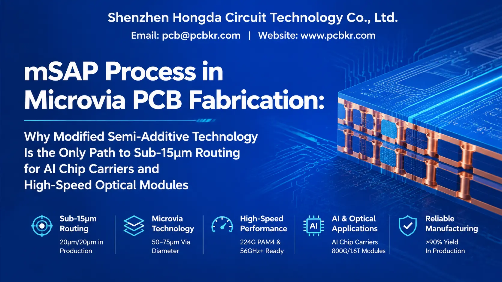
mSAP Process in Microvia PCB Fabrication: Why Modified Semi-Additive Technology Is the Only Path to Sub-15μm Routing for AI Chip Carriers and High-Speed Optical Modules
Introduction: The Subtractive Etching Ceiling and Why mSAP Became Unavoidable in 2026
If you are a hardware procurement manager sourcing microvia PCBs for AI infrastructure in 2026, you have likely encountered a frustrating reality: your design team specifies 20 μm line/space for a GPU carrier board or 25 μm for an 800G optical module, and your incumbent PCB supplier responds with a 12-week lead time, a 40% yield penalty, or a flat refusal. The reason is not supplier incompetence. It is physics.
Traditional subtractive PCB etching—the industry workhorse for six decades—has hit a hard wall. At line/space dimensions below 30 μm, isotropic etch undercut transforms rectangular traces into trapezoidal profiles. Impedance control drifts beyond acceptable limits. Yield collapses. And for applications like AI chip carrier boards, CoWoP (Chip-on-Wafer-on-PCB) packaging, and 1.6T optical transceivers, 30 μm is no longer adequate.
Enter mSAP (Modified Semi-Additive Process)—a manufacturing methodology that has shifted from niche IC substrate fabrication to mainstream microvia PCB production in the span of 24 months. In 2026, mSAP is not an option for high-end designs. It is the baseline.
This article explains, from a procurement and manufacturing engineering perspective, why mSAP process PCB technology has become the definitive solution for fine-line microvia fabrication in High-Density Interconnect (HDI) Microvia PCB Manufacturing | mSAP & SAP Capabilities for AI Server and HPC Applications. We will walk through the process mechanics, compare mSAP against subtractive etching and full SAP, examine real-world applications in AI servers and optical modules, and provide a decision framework for qualifying an mSAP PCB manufacturer that can actually deliver—not just quote.
At Shenzhen Hongda Circuit Technology Co., Ltd. , our mSAP line has been in continuous production since 2024, with 2026 capacity expansion targeting 20 μm/20 μm line/space in volume and 8 μm/8 μm qualified for substrate-like PCB (SLP) builds. The data, equipment specifications, and process controls described below reflect our actual production floor—not aspirational marketing.
What Is the mSAP Process? A Step-by-Step Manufacturing Breakdown
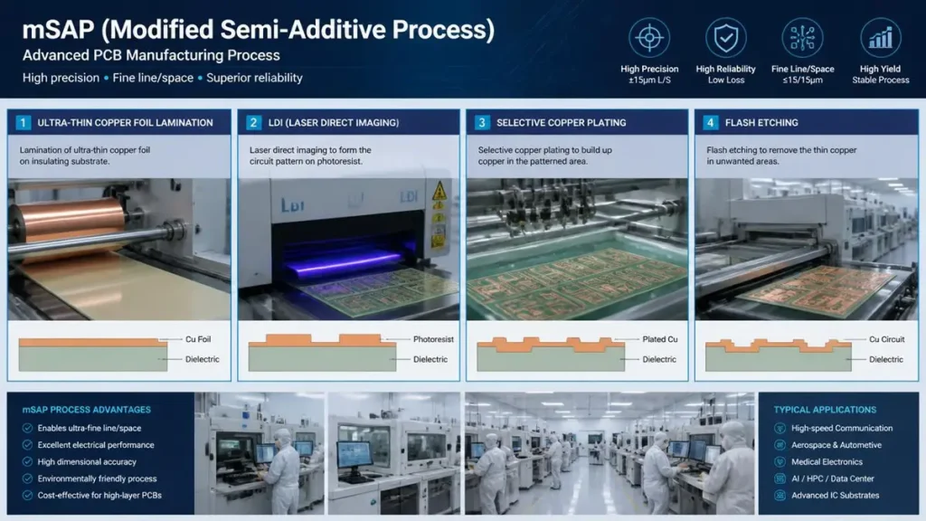
mSAP Manufacturing Process Step-by-Step Breakdown – Hongda Circuit
The Fundamental Principle: Build Up, Not Etch Down
The modified semi-additive process (mSAP) reverses the logic of traditional PCB fabrication. Instead of starting with thick copper and removing material, mSAP starts with minimal copper and adds material only where traces are needed.
Here is the exact process sequence as executed on our production line:
Step 1: Ultra-Thin Copper Foil Lamination We begin with a 1.5–3 μm thin copper foil laminated onto the dielectric substrate—typically M7N or M8-grade low-loss material for AI server applications, or standard high-Tg FR-4 for cost-optimized builds. This is roughly one-tenth the thickness of standard 18 μm copper foil used in subtractive processes. The thin starting layer is the critical enabler: it means the subsequent flash etch removes almost no material from the final traces.
Step 2: Surface Preparation and Photoresist Application The thin copper surface undergoes micro-roughening to enhance photoresist adhesion. We apply dry-film photoresist (DFR) at 15–20 μm thickness using automated roller laminators. The resist must be completely free of pinholes and particulate contamination—any defect at this stage will translate into a trace break or short in the final circuit.
Step 3: Laser Direct Imaging (LDI) Patterning This is where precision becomes non-negotiable. Our SCREEN Ledia LDI system exposes the photoresist using a 405 nm laser diode array with ±1.5 μm registration accuracy across a 24-inch panel. Unlike traditional phototools (film masks), LDI eliminates mask stretch, dust artifacts, and alignment drift. For a 20 μm/20 μm design, a 3 μm misalignment represents a 15% geometric error—unacceptable for impedance-controlled differential pairs.
Step 4: Selective Pattern Plating With the resist defining the trace channels, we electroplate copper into the open areas. Our 3-in-1 horizontal plating line—integrating desmear, electroless copper activation, and electrolytic copper deposition—builds trace height to the target value, typically 15–20 μm for AI server signal layers. The plating chemistry uses a proprietary suppressor/accelerator/leveler (SAL) additive package that ensures ±3% thickness uniformity across the panel, verified by real-time laser displacement sensors.
Step 5: Photoresist Stripping and Flash Etch After plating, the photoresist is chemically stripped, exposing the thin seed copper between traces. A gentle flash etch—typically 10–15 seconds in a sulfuric acid/hydrogen peroxide bath—removes this 1.5–3 μm seed layer without significantly attacking the 18–20 μm plated traces. The result: near-vertical trace sidewalls with aspect ratios (trace height to base width) approaching 1:1, compared to 0.6:1 for subtractive etching.
Step 6: Automated Optical Inspection (AOI) and Metrology Every mSAP panel undergoes 100% AOI using 3 μm resolution line-scan cameras, followed by SEM microsection analysis on sample coupons. We measure trace width, sidewall angle, copper grain structure, and surface roughness. Data is fed back into our process control system for real-time adjustment.
Why This Sequence Matters for Microvia PCB Integration
The mSAP process is not merely a fine-line technique—it is the natural companion to High-Density Interconnect (HDI) Microvia PCB Manufacturing. In a high-density interconnect (HDI) build, microvias terminate on pads that must connect to traces as narrow as 20 μm. If those traces are fabricated via subtractive etching, the trapezoidal profile and undercut create a mechanical stress concentration at the via-to-trace junction. Under thermal cycling, this is where cracks initiate.
mSAP’s vertical sidewalls and precise geometry distribute stress uniformly. When combined with copper-filled microvias and proper aspect ratio control, the mSAP-microvia pairing achieves reliability metrics that subtractive processes cannot approach.
mSAP vs. Subtractive Etching: A Technical and Economic Comparison
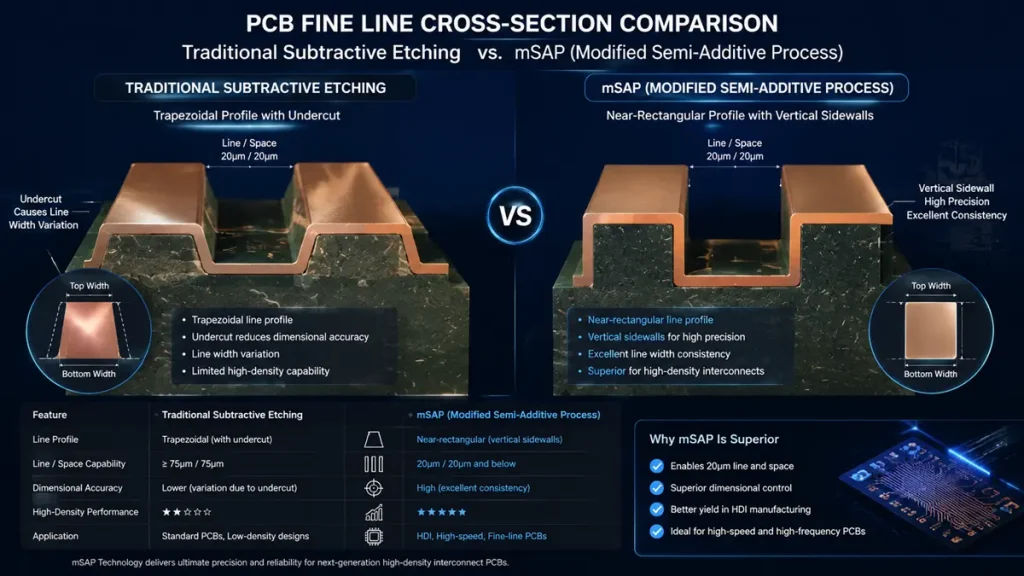
PCB Fine-Line Cross-Section Comparison: Subtractive Etching vs. mSAP Process – Hongda Circuit
The Etching Undercut Problem: Why 30 μm Is the Subtractive Floor
In subtractive etching, the etchant attacks copper both vertically and laterally. The degree of undercut depends on:
• Etchant chemistry: Alkaline ammonia etchants are more isotropic than acid-based alternatives
• Copper thickness: Thicker foil requires longer etch time, increasing lateral attack
• Resist adhesion: Poor adhesion allows etchant seepage under the resist edge
• Etch factor: The ratio of vertical etch depth to lateral undercut, typically 2:1 to 3:1
For a standard 18 μm copper foil with a 2.5:1 etch factor, the lateral undercut is 7.2 μm per side. To achieve a 30 μm top-width trace, the resist opening must be 44.4 μm. At 20 μm target width, the resist opening shrinks to 34.4 μm—below the practical resolution of most imaging systems, and mechanically fragile during processing.
The result is a trapezoidal trace profile with a top width of 20 μm, base width of 34.4 μm, and unpredictable impedance. For 224G PAM4 signaling, where impedance tolerance is ±5% (typically 85 ± 4.25 Ω for differential pairs), this variability is catastrophic.
Side-by-Side Process Comparison
| Parameter | Subtractive Etching | mSAP (Modified Semi-Additive) |
|---|---|---|
| Starting Copper | 18–35 μm standard foil | 1.5–3 μm ultra-thin foil |
| Line/Space Production Limit | 50–60 μm (reliable); 40 μm (marginal) | 20–30 μm (production); 15 μm (qualified) |
| Trace Profile | Trapezoidal, 60–70° sidewall angle | Near-rectangular, 85–88° sidewall angle |
| Impedance Control (1σ) | ±8–10% | ±3–5% |
| Etch Undercut | 6–10 μm per side | <0.5 μm per side |
| BGA Pitch Support | 0.4–0.5 mm | 0.25–0.3 mm |
| Relative Processing Cost | 1.0× (baseline) | 1.8–2.5× |
| Typical Applications | Standard multilayer, power distribution | AI server, optical module, smartphone SLP |
When Subtractive Etching Still Makes Sense
Despite mSAP’s advantages, subtractive etching remains the correct choice for:
• Power distribution layers with 2–6 oz copper, where fine-line capability is irrelevant
• Ground planes where trace geometry is non-critical
• Cost-optimized consumer electronics where 50 μm line/space is adequate
• Prototypes with relaxed timelines where mSAP capacity is better reserved for production
At Hongda Circuit, we practice hybrid manufacturing: mSAP for signal layers requiring fine-line precision, subtractive etching for power and ground layers. This approach reduces overall board cost by 15–20% compared to full mSAP builds while preserving signal integrity where it matters.
mSAP in Action: 2026 Applications Driving Adoption

mSAP PCB Applications in AI Server Motherboards and Optical Modules – Hongda Circuit
AI Chip Carrier Boards and CoWoP Packaging: The SLP Revolution
The most consequential packaging trend of 2026 is CoWoP (Chip-on-Wafer-on-PCB)—NVIDIA’s reported architecture for the Rubin platform, where the GPU die and HBM stacks sit on an interposer that is directly attached to the system PCB, bypassing the traditional IC substrate. This eliminates one packaging tier, reduces signal path length, and improves power delivery—but it places unprecedented demands on the PCB itself.
CoWoP requires Substrate-Like PCB (SLP) technology, which is essentially mSAP taken to its extreme, all AI board stackup standards are detailed inside Microvia PCBs for AI Servers and HPC Infrastructure: Advanced HDI Manufacturing & Any-Layer Design Guidelines. Line/space specifications for CoWoP test vehicles in 2026 are 8–12 μm on build-up layers, with microvia diameters of 50–75 μm and stacked via structures up to 4 layers deep. These are not incremental improvements over standard HDI; they are IC substrate specifications manufactured on PCB-scale panels.
At Shenzhen Hongda Circuit Technology, we have qualified 8 μm/8 μm mSAP line/space for SLP builds targeting CoWoP and similar advanced packaging applications. Our process uses:
• Picosecond laser drilling for 50 μm microvias in thin build-up dielectrics
• Advanced LDI with sub-micron alignment for 8 μm feature resolution
• Enhanced plating chemistry with grain refiners to prevent copper dendrite formation at fine pitches
• Class 1000 cleanroom environment for SLP processing, preventing particulate-induced shorts
800G and 1.6T Optical Modules: mSAP as the Enabler of Silicon Photonics
The optical transceiver market is experiencing explosive growth. According to industry analysis, 800GbE optical module shipments are ramping rapidly in 2026, growing 146% year-over-year to 52.8 million units, while 1.6TbE modules are scaling from late Q3 2026, surging 1,200% to 28.6 million units. Each of these modules contains a PCB that routes high-speed electrical signals from the switch ASIC to the optical engine.
The challenge: 800G modules use 12–14 layer PCBs with Any-Layer (6-2-6) structures, while 1.6T modules require 14–16 layers with Any-Layer (7-2-7) stackups. With total PCB thickness capped at approximately 1 mm, the line/space must shrink to 25–30 μm to maintain controlled impedance in the available routing area. Subtractive etching cannot reliably achieve this density.
mSAP is the solution. For an 800G optical module PCB, we typically fabricate 4–8 mSAP layers on the signal build-up layers, with standard subtractive processing for the thicker core layers. For 1.6T modules, the mSAP layer count increases to 8–14 layers, with M7N-M8 grade low-loss laminates to manage insertion loss at 56 GHz Nyquist frequencies.
Our production data from Q2 2026 shows >92% first-pass yield on 800G optical module PCBs with 25 μm/25 μm mSAP line/space, verified through 100% electrical test and S-parameter coupon analysis.
AI Server Motherboards and Switch Fabrics: mSAP for 224G PAM4 Escape Routing
Beyond chip carriers and optical modules, mSAP PCB technology is increasingly required for AI server motherboards and switch fabric boards. A modern AI server motherboard may contain four or more CPU/GPU sockets, each with a 0.35 mm pitch BGA package containing 5,000+ pins. Escape routing from these packages demands trace widths of 20–25 μm to avoid layer count inflation.
For 224G PAM4 switch fabrics, the situation is even more constrained. A 51.2T switch ASIC may have 128 ports of 400G or 64 ports of 800G, with SerDes channels operating at 112 Gbaud. The BGA pitch for these devices is often 0.8–1.0 mm, but the escape routing density is extreme due to the sheer number of differential pairs. mSAP enables clean escape patterns without the dog-bone via stubs that degrade signal integrity in subtractive designs.
Quality Control in mSAP Manufacturing: What Procurement Teams Must Verify
Flash-Etch Uniformity: The Silent Yield Killer
The most common failure mode in mSAP production is non-uniform flash etch. If the seed layer is not completely removed between traces, residual copper creates shorts. If the etch is too aggressive, it attacks the plated traces, reducing cross-sectional area and increasing resistance.
At Hongda Circuit, we monitor flash-etch uniformity using laser displacement sensors that scan the panel surface before and after etching, measuring seed layer removal rate at 256 points across the panel. Our specification is ±5% etch rate uniformity; any panel exceeding this limit is flagged for engineering review.
LDI Registration Accuracy: The Geometry Gatekeeper
At 20 μm line/space, a 3 μm misalignment between the photoresist image and the underlying microvia pad creates a 15% geometric error. In the worst case, the trace may miss the pad entirely, creating an open circuit that is not detectable until electrical test—after all processing is complete.
Our LDI system maintains ±1.5 μm registration accuracy through:
• Panel-edge fiducial recognition with sub-pixel interpolation
• Real-time thermal compensation for panel expansion during exposure
• Automatic scale factor adjustment based on measured material shrinkage
• Multi-point alignment referencing both panel edges and internal fiducials
Plating Thickness Distribution: The Impedance Variable
Copper plating thickness directly affects trace cross-section and therefore impedance. A 15 μm target thickness with ±10% variation creates a 3 μm swing, which shifts impedance by approximately 2–3 Ω for a 100 Ω differential pair. Our plating line achieves ±3% thickness uniformity through:
• Cathode agitation with programmable oscillation profiles
• Real-time chemistry analysis with automatic additive replenishment
• Dummy panel loading to normalize current density at panel edges
• Cross-panel bussing to eliminate current crowding
In-House Metrology: Why Outsourced QA Fails for mSAP
mSAP quality cannot be verified with standard optical microscopy. At minimum, a qualified mSAP PCB manufacturer must maintain:
• Scanning Electron Microscopy (SEM) for trace profile and sidewall angle measurement
• Focused Ion Beam (FIB) cross-sectioning for via-to-trace interface analysis
• X-ray fluorescence (XRF) for plating thickness verification
• TDR (Time Domain Reflectometry) for impedance validation
At Hongda Circuit, all of these capabilities are in-house. We do not outsource microsection analysis. This eliminates the 24–48 hour delay of external lab turnaround and ensures that quality data is available for real-time process adjustment.
Procurement Decision Framework: Qualifying an mSAP PCB Supplier
The Five Critical Questions Every Buyer Should Ask
When evaluating an mSAP PCB supplier for AI server, optical module, or advanced packaging applications, do not settle for capability statements. Demand evidence.
Question 1: What is your production-qualified line/space, and what is your yield at that geometry? A supplier quoting 15 μm but achieving 60% yield is not a production partner—they are a prototype shop. At Hongda Circuit, our production-qualified mSAP line/space is 20 μm/20 μm with >90% first-pass yield, and we have qualified 8 μm/8 μm for SLP builds with dedicated process lanes.
Question 2: What is your flash-etch uniformity specification, and how is it monitored? If the supplier cannot provide a numerical uniformity target with real-time monitoring methodology, their mSAP process is not under statistical control. Our specification is ±5% across the panel, measured by laser displacement sensors.
Question 3: What LDI registration accuracy do you maintain on a 24-inch panel? At fine-line geometries, registration is everything. Our SCREEN Ledia system maintains ±1.5 μm across the full panel, verified on every lot with automated fiducial measurement.
Question 4: Do you have in-house SEM, TDR, and XRF capability? Outsourced metrology introduces delays and quality blind spots. We maintain all three capabilities in-house, with SEM microsections available within 4 hours of sample request.
Question 5: What is your track record with AI server or optical module customers? Process capability is necessary but not sufficient. Production discipline—on-time delivery, lot traceability, change control, and documentation—is what separates a qualified supplier from a capable one. We have shipped mSAP-enabled boards for 800G optical modules and AI server GPU carriers since 2024, with full lot traceability and PPAP documentation available for automotive and aerospace customers.
Frequently Asked Questions: mSAP Process Procurement
mSAP vs. SAP—Which Process Should I Specify for My Design?
mSAP (Modified Semi-Additive Process) starts with 1.5–3 μm thin copper foil and achieves 15–30 μm line/space in production. It is the standard for advanced HDI, AI server boards, optical modules, and substrate-like PCBs.
SAP (Semi-Additive Process) starts with <1 μm electroless copper and achieves 5–15 μm line/space. It requires substrate-grade cleanrooms and DUV lithography, making it significantly more expensive and limited to IC substrates and interposers.
Recommendation: Specify mSAP for all designs requiring 15–30 μm line/space. Only specify SAP if you need sub-15 μm routing for chiplet integration or advanced packaging. At Hongda Circuit, we offer both processes with full in-house capability.
How Does mSAP Affect PCB Cost, and What Is the ROI?
mSAP adds 1.8–2.5× processing cost compared to subtractive etching for the layers that use it. However, this must be evaluated against total system cost:
• Layer count reduction: mSAP can eliminate 2–4 layers in a dense BGA escape design, reducing laminate cost by 15–25%
• Yield improvement: Higher first-pass yield reduces rework, scrap, and schedule risk
• Performance assurance: Boards that meet signal integrity specs on the first build avoid costly respins • Reliability: mSAP’s vertical trace profiles reduce thermal cycling failures, lowering field return costs
For most AI server and optical module designs, the net cost impact of mSAP is neutral to 15% higher when total system cost is considered, while the risk reduction is substantial.
What Materials Work Best with mSAP?
mSAP is compatible with all standard PCB laminates, but the best results require:
• Low-profile copper foil (<3 μm Rz surface roughness) for uniform seed layer adhesion
• Dimensionally stable dielectrics with low CTE mismatch to copper
• Low-loss materials (M7, M7N, M8) for high-speed applications • Thin build-up dielectrics (20–40 μm) for fine-line layers
We maintain qualified material lists (QML) for mSAP processing, with incoming inspection of Dk/Df, Tg, and CTE for every lot.
Can mSAP Be Combined with Standard Subtractive Layers in a Hybrid Build?
Yes, and this is our recommended approach for most designs. A typical AI server motherboard might use:
• mSAP on outer build-up layers (L1–L2, L(n)–L(n-1)) for BGA escape and fine-pitch routing
• Subtractive etching on internal core layers for power, ground, and low-speed signals • mSAP on selective internal layers only where density demands it
This hybrid approach reduces overall cost by 15–20% compared to full mSAP while preserving signal integrity where it matters.
What Is the Typical Lead Time for mSAP PCB Prototypes?
Standard industry lead times for mSAP PCB prototypes range from 10–15 working days for simple 4–8 layer builds, faster fast-track options are introduced in Custom Microvia PCB Fabrication & Quick-Turn HDI Prototyping: A 2026 Procurement Decision Framework. and 15–20 days for complex HDI with mSAP. At Hongda Circuit, we offer:
• 5-day turnaround for 10–16 layer mSAP builds with copper-filled microvias
• 7-day turnaround for 20+ layer hybrid builds with mSAP signal layers
• 24-hour DFM feedback on all mSAP designs • 48-hour first article for qualified repeat customers
Our dedicated mSAP production lane ensures that urgent prototypes are not delayed by lower-priority volume orders.
Conclusion: mSAP Is Not the Future—It Is the Present
The transition from subtractive etching to mSAP process PCB technology is not a speculative trend in advanced High-Density Interconnect (HDI) Microvia PCB Manufacturing. It is a completed transition for the segments of the market that matter most: AI servers, optical transceivers, advanced packaging, and high-performance mobile devices. In 2026, a PCB supplier without qualified mSAP capability is simply not a viable partner for designs above 30 μm line/space.
The procurement imperative is clear: verify capability, verify yield, verify metrology, and verify track record. Do not accept capability statements at face value. Demand data. Demand microsections. Demand S-parameter reports. The suppliers who can provide these without hesitation are the ones who can actually build your board.
At Shenzhen Hongda Circuit Technology Co., Ltd., our mSAP line is not a pilot project or a marketing claim. It is a production reality, shipping boards to AI infrastructure and optical module customers with the documentation, traceability, and quality discipline that B2B procurement teams require.
Ready to evaluate mSAP for your next design?
Submit your Gerber files and stackup requirements for a complimentary DFM review and mSAP feasibility assessment. Our engineering team will analyze your design for manufacturability, recommend the optimal process flow (mSAP, hybrid, or subtractive), and provide a detailed quotation within 30 minutes.
📧 Email: sales@pcbkr.com
📧 Engineering: pcb@pcbkr.com
📞 Phone: +86 0755 23720053
🌐 Website: www.pcbkr.com
📍 Address: Room 1608-1610, Research Development Comprehensive Building, Baoyunda Logistics Center, Baoan, Shenzhen, China
About Author
David Chen https://www.linkedin.com/in/pcbcoming
David Chen boasts an extensive professional background in PCBA manufacturing, PCBA testing, and PCBA optimization, with specialized expertise in high-precision PCBA fault analysis and rigorous PCBA reliability testing. The author has worked with high-layer-count server PCB fabrication, ultra-low-loss backplane stackups, and thermo-mechanical reliability optimization for AI infrastructure projects involving 112G and 224G PAM4 architectures. Skilled in complex circuit design and cutting-edge advanced PCB manufacturing processes, he delivers solutions that elevate product durability and performance across industrial applications. His technical articles focusing on PCBA manufacturing workflows and testing methodologies are widely cited by industry peers, research institutions, and technical platforms, solidifying his reputation as a recognized technical authority in the global circuit board manufacturing sector.