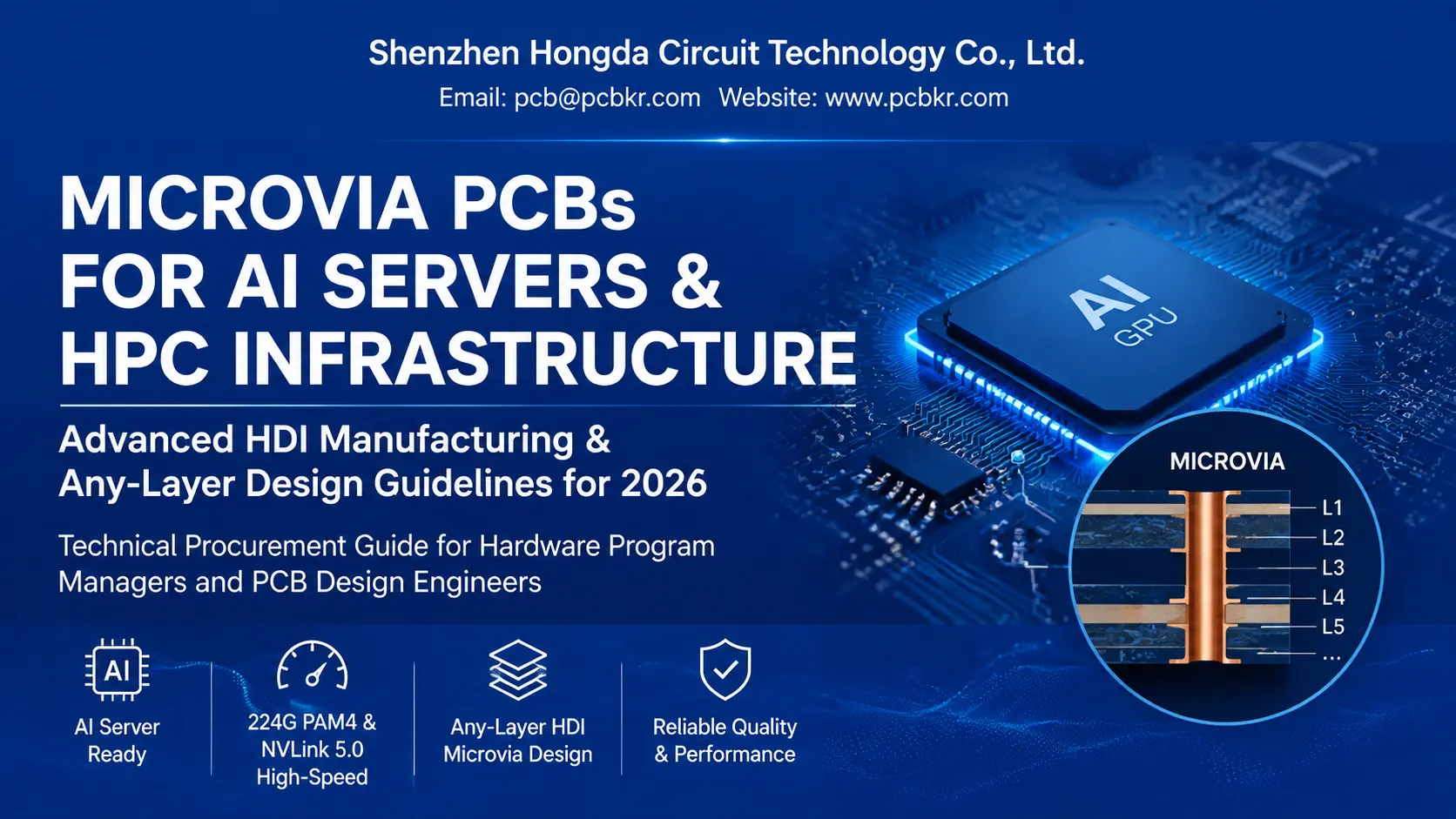
Microvia PCBs for AI Servers and HPC Infrastructure: Advanced HDI Manufacturing & Any-Layer Design Guidelines
From Generic HDI to Application-Specific Microvia Architecture
The preceding pillar guide, High-Density Interconnect (HDI) Microvia PCB Manufacturing | mSAP & SAP Capabilities for AI Server and HPC Applications, established the manufacturing fundamentals of HDI microvia technology—laser drilling thresholds, mSAP versus SAP process economics, and the certification landscape that separates qualified suppliers from marketing brochures. This resource narrows the aperture to the highest-stakes application domain in contemporary PCB procurement: AI server infrastructure and high-performance computing (HPC) platforms.
The global AI server HDI PCB market reached USD 2.50 billion in 2025 and is projected to expand at a 12.7% CAGR through 2035, with microvia HDI PCBs commanding a 45% revenue share. The procurement professional evaluating suppliers in 2026 is no longer merely sourcing a commodity board. You are qualifying a thermal-electrical-mechanical system whose failure modes—via barrel cracking under 1,000 W GPU thermal cycling, impedance drift across a 104-layer backplane, or insertion-loss collapse at 56 GHz—can derail an entire AI cluster deployment.
This guide is structured along two parallel decision tracks that reflect how buyers actually search and evaluate:
Cluster 2.1 — Strategic Procurement Track: For hardware program managers sourcing AI server microvia PCBs, GPU board microvia technology, and HDI PCB microvia technology at the system level. We dissect how Blackwell/Hopper architectures drive stackup decisions, why 224G PAM4 signal integrity mandates redefine supplier capability thresholds, and how to structure an RFI that exposes manufacturing weaknesses before they become field failures.
Cluster 2.2 — Engineering Design Track: For PCB layout engineers and hardware architects who need any-layer HDI microvias PCB design rules that compress NPI timelines. We provide actionable stackup parameters, impedance control standards, and DFM guardrails that prevent the iterative redesign loops that kill procurement schedules.
Both tracks converge on a single truth: in the current supply-constrained environment, where AI demand has pushed standard PCB lead times beyond 80 days and material costs have surged 35% year-over-year, the wrong supplier choice is not merely expensive—it is existential.
Cluster 2.1: AI Server Microvia PCB — Architecture and Signal Integrity Demands for Blackwell & Hopper Platforms
GPU Board Microvia Technology: From H100 to B200 Baseboard Evolution
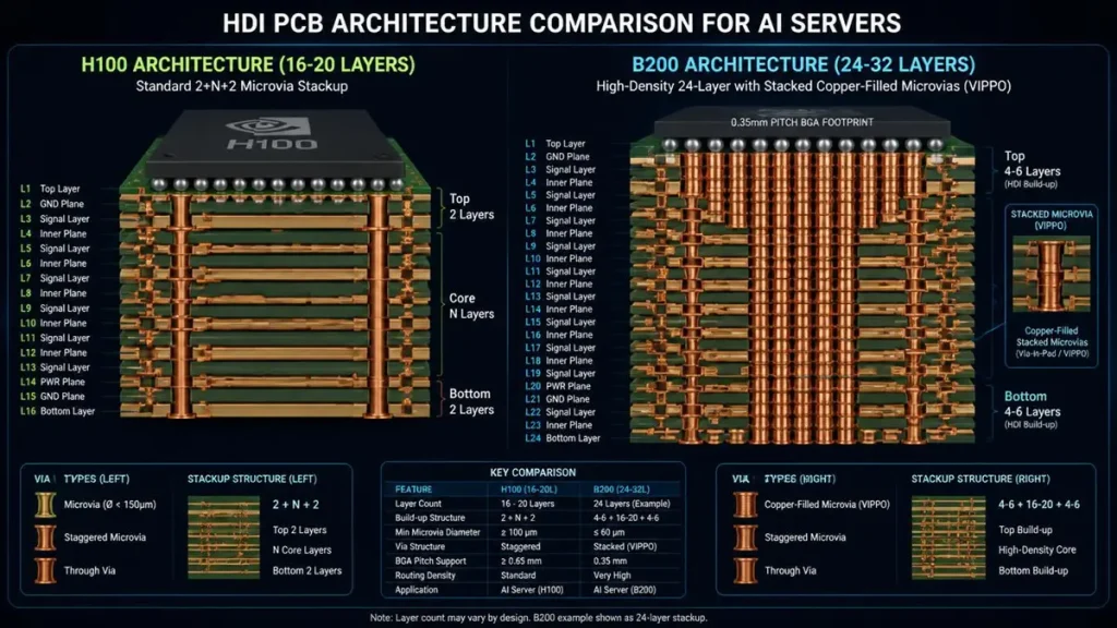
H100 vs. B200 AI Server HDI PCB Microvia Architecture & Stackup Comparison
The transition from NVIDIA Hopper (H100/H200) to Blackwell (B200/GB200) represents a discontinuous jump in PCB complexity, not an incremental refinement. Where an H100 baseboard typically required 16–20 layers with 1+N+1 or 2+N+2 HDI build-up, the B200 baseboard demands 24–32 layers in advanced High-Density Interconnect (HDI) Microvia PCB Manufacturing driven by three architectural stressors:
NVLink 5.0 at 200 Gb/s per lane requires dedicated signal layers that cannot share routing space with power planes due to crosstalk budgets tighter than −35 dB at 56 GHz Nyquist.
PCIe Gen6 at 64 GT/s PAM4 introduces 85 Ω differential impedance targets with intra-pair skew below 3 ps—specifications that expose every micron of trace-width variation.
Dual-die CoWoS-L packaging expands the BGA footprint relative to SXM5, forcing finer escape routing under the socket perimeter where 0.35 mm pitch arrays leave no room for conventional dog-bone fan-out.
For procurement teams, this means the GPU board microvia technology specification cannot be delegated to a standard HDI datasheet. the microvia architecture must support stacked copper-filled vias (VIPPO) under 0.35 mm pads, all laser hole production specs are covered in Laser Microvia Drilling Technology and Capabilities: UV, CO₂, and Femtosecond Systems for Precision HDI PCB Fabrication. with aspect ratios held to 1:1 or below per IPC-2226, and with void rates under 5% verified by 3D X-ray on every production lot. At Shenzhen Hongda Circuit Technology, our Mitsubishi UV/CO₂ laser drilling systems achieve ±5 μm positional accuracy on 75–100 μm microvias, with copper fill validated on Nordson DAGE 3D AXI systems at 5% void-detection sensitivity. These are not aspirational specifications—they are production parameters locked in our 2026 process control plan.
HDI PCB Microvia Technology for 224G PAM4 and NVLink 5.0 Channels
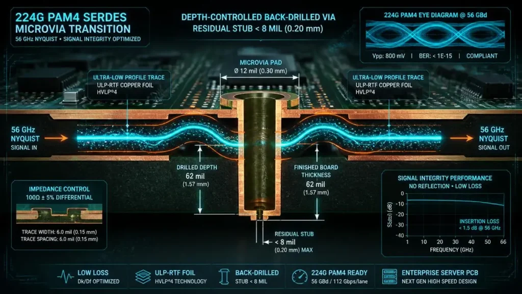
224G PAM4 SerDes Microvia Transition & Back-Drilling Residual Stub (< 8 mil) Analysis
At 224G PAM4, the via stub is no longer a secondary parasitic; it is a channel-killer. A 50-mil via stub resonates at approximately 15 GHz, and its third harmonic at 45 GHz lands directly inside the 56 GHz Nyquist band, producing a 6–10 dB insertion-loss notch that no equalization can recover.
Procurement-critical 224G PAM4 manufacturing requirements:
Back-drilling residual stub: ≤ 8 mil (0.20 mm), verified by destructive cross-section on panel coupons. Our depth-controlled back-drilling process maintains ±2 mil tolerance with 100% depth-measurement logging per panel.
Copper foil specification: Ultra-low-profile reverse-treated foil (ULP-RTF) with Rz ≤ 0.7 μm. Standard HTE copper at Rz 3.0–4.0 μm introduces approximately 3.3 dB of excess loss at 56 GHz—consuming the entire design margin.
Material qualification: Panasonic Megtron 7 (Df ~0.002 at 10 GHz) or Isola Tachyon 100G for NVLink 5.0 signal layers. Standard FR-4 with Df ~0.020 generates 32 dB of dielectric loss on a 40-inch channel—exceeding the entire IEEE 802.3df budget.
Ground via co-location: Every 224G signal via transition must be accompanied by a ground stitching via within 12 mil to suppress common-mode conversion at the layer transition.
When qualifying an HDI PCB microvia technology supplier for 224G channels, demand S-parameter test reports from actual production boards—not simulation decks—showing insertion loss and return loss through 56 GHz. Our 224G PAM4 process, validated in continuous production since Q1 2025 and updated with 2026 laminate qualifications, includes first-article impedance and IL/RL coupon reports as standard deliverables.
Any-Layer HDI Stackup for AI Accelerator OAM/UBB Modules
The OAM (OCP Accelerator Module) and UBB (Universal Baseboard) form factors for AI accelerators represent the most density-constrained PCB applications outside of IC substrates. With 1,500+ I/Os per accelerator and BGA pitches at 0.35 mm, any-layer HDI—where microvias connect any adjacent layer pair without a fixed core constraint—becomes mandatory.
Any-layer HDI procurement specifications for AI accelerators:
| Parameter | Specification | Rationale |
|---|---|---|
| Microvia diameter | 50–75 μm | Enables escape routing under 0.35 mm pitch BGA |
| Aspect ratio | ≤ 1:1 | Ensures void-free copper plating at high aspect ratios |
| Build-up dielectric | 40–60 μm (106 prepreg, ≥65% resin content) | Clean laser ablation, minimal glass fiber protrusion |
| Line/space | 30/30 μm (mSAP) or 20/20 μm (advanced mSAP), full mSAP production workflow is explained in mSAP Process in Microvia PCB Fabrication: Why Modified Semi-Additive Technology Is the Only Path to Sub-15μm Routing for AI Chip Carriers. | Matches BGA escape density requirements |
| Layer count | 20–28 layers | Supports HBM3e routing, power planes, and NVLink/PCIe signal layers |
| Registration accuracy | ±25 μm layer-to-layer | Prevents microvia misalignment in stacked configurations |
Our any-layer HDI line operates with SCREEN Ledia LDI exposure at ±1.5 μm registration accuracy, coupled with a 3-in-1 horizontal plating line (desmear + electroless + electrolytic copper) that improves throughput by 40% while maintaining the uniformity required for 20 μm/20 μm mSAP production. For substrate-like PCB (SLP) builds targeting AI edge devices, we have qualified 8 μm/8 μm line/space capability.
Power Integrity and Thermal Management in High-Layer-Count Backplanes
The B200’s 1,000 W TDP and dual-die architecture demand a power delivery network (PDN) of unprecedented complexity: 15–25 distinct power rails, with VCORE at ~0.85–0.9 V and currents exceeding 800 A. The PCB must deliver this current with end-to-end copper plane resistance below 0.2 mΩ and PDN impedance below 0.1 mΩ from DC to 100 MHz.
Backplane-specific microvia considerations:
Power via arrays: High-current power vias require larger diameters (0.3–0.5 mm) or dense microvia arrays to distribute current without creating thermal hot spots. Our facility produces 104-layer orthogonal backplane PCBs with interlayer registration held within ±25 μm to resist press-fit connector installation stresses.
Thermal vias: Microvia arrays under VRM phases and GPU sockets improve thermal conductivity to heatsink mounting planes. We integrate copper coin and cavity routing for localized thermal management.
Flat-weave glass fabrics: To eliminate the glass-weave effect—where differential pairs crossing glass bundles experience periodic impedance perturbations—we deploy spread-glass and flat-weave laminates (e.g., Panasonic Megtron 7 with 1067 glass style) on all 224G signal layers.
Procurement Decision Framework: Evaluating AI Server Microvia PCB Suppliers
When issuing an RFI for AI server microvia PCB manufacturing, structure your technical inquiry around these verification points:
Process Control Depth – What is your laser drilling positional accuracy and Cpk? (Target: ±5 μm with Cpk ≥ 1.33) – What is your maximum qualified microvia aspect ratio for copper-filled vias? (Target: 15:1 for blind vias, 1:1 for build-up microvias) – What is your microvia void rate, and is verification performed by 3D X-ray or cross-section sampling? (Target: <1% void rate, 100% 3D AXI coverage)
High-Speed Qualification – What 224G PAM4 production history do you have? Demand customer references and first-article test reports. – What low-loss materials do you stock with lot-traceable Dk/Df data at 10 GHz? – What is your impedance control tolerance, and is it verified by TDR on production coupons? (Target: ±5% standard, ±3% premium)
Quality System Maturity – What is your default IPC class for HDI builds? (Class 3 should be baseline for AI server applications; Class 3A available upon request) – What is your internal scrap rate and customer return rate in ppm? – Do you maintain lot traceability from raw laminate to finished PCB with material certificates?
Supply Chain Resilience – In the current environment of 80+ day lead times, what safety stock do you maintain on Megtron 7, Tachyon 100G, and other AI-grade laminates? – What is your fast-track prototype capability? (Our standard: 48-hour turnaround for 4–8 layer HDI, 5-day for 10–16 layer mSAP, 7-day for 20+ layer backplanes)
Cluster 2.2: Any-Layer HDI Microvias PCB Design — Stackup Architecture and Impedance Control Standards
Microvia Aspect Ratio and Capture Pad Sizing Rules per IPC-2226
The foundation of any any-layer HDI microvias PCB design is disciplined adherence to microvia physics. IPC-2226 specifies a maximum aspect ratio of 1:1 (depth divided by diameter) for reliable copper plating. In practice, designing at the 1:1 limit leaves no margin for dielectric thickness variation. Our DFM protocol mandates a 10% engineering margin:
| Microvia Diameter | Maximum Dielectric Thickness | Recommended Design Thickness | Capture Pad (Min) | Capture Pad (Recommended) |
|---|---|---|---|---|
| 100 μm (4 mil) | 100 μm | ≤80 μm | 250 μm | 300 μm |
| 75 μm (3 mil) | 75 μm | ≤60 μm | 200 μm | 250 μm |
| 50 μm (2 mil) | 50 μm | ≤40 μm | 150 μm | 180 μm |
Capture pad sizing formula: Microvia diameter + 150 μm minimum. This accounts for laser position tolerance (±50 μm), copper plating thickness (20–25 μm), and a minimum 50 μm annular ring for structural integrity under thermal cycling.
Violating the aspect ratio rule is the single most common cause of microvia field failures. When the ratio exceeds 1:1, plating solution cannot circulate effectively to the via bottom corner, creating a thin copper zone that cracks under CTE-mismatch stress. A 1.2:1 aspect ratio reduces mean-time-to-failure by approximately 40% compared to 1:1 in IPC-2226 reliability testing.
Stacked vs. Staggered Microvia Configuration: Reliability vs. Density Trade-offs
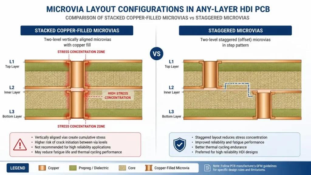
AI Server Microvia PCB Stackup & HDI Architecture
The choice between stacked and staggered microvias is not merely a layout preference; it is a reliability contract with your fabricator.
| Configuration | Thermal Cycles to Failure (IPC-2226) | Relative Reliability | Area Efficiency | Best Application |
|---|---|---|---|---|
| Single microvia (1-level) | 1,000+ cycles | 100% baseline | 1 via per connection | Standard HDI, outer layer escape |
| Staggered (2-level) | 800–1,000 cycles | 80–100% | 2 vias, offset positions | Automotive ADAS, aerospace, high-reliability AI edge |
| Stacked, copper-filled (2-level) | 500–800 cycles | 50–80% | 1 XY position | AI server GPU carriers, smartphones, density-constrained designs |
| Stacked, copper-filled (3-level) | 300–500 cycles | 30–50% | 1 XY position | Avoid unless absolutely necessary |
Design guidance for procurement teams:
For automotive or mission-critical AI inference platforms under IATF 16949, mandate staggered microvias. The 1,000-cycle thermal shock requirement (−40°C to +125°C) is challenging for stacked configurations.
For AI training clusters where board replacement is operationally manageable and density is paramount, stacked copper-filled microvias with VIPPO are acceptable and economically necessary. Our plating line achieves void-free copper fill at aspect ratios up to 20:1 using proprietary suppressor/accelerator/leveler chemistry, followed by precision planarization.
Never specify 3-level stacked microvias without a reliability waiver and accelerated life-test data. The cumulative thermal expansion stress at the via base exceeds the fracture threshold of standard copper barrels unless specialized plating and annealing protocols are employed.
Impedance Control Standards for 85 Ω and 100 Ω Differential Pairs
In any-layer HDI designs for AI servers, impedance is not a post-layout verification step—it is a stackup design parameter that must be locked before component placement begins.
Hongda’s 2026 impedance control matrix for any-layer HDI:
| Interface | Differential Impedance | Tolerance (Standard) | Tolerance (Premium) | Verification Method |
|---|---|---|---|---|
| PCIe Gen6 | 85 Ω | ±5% | ±3% | TDR on production coupons + 2D field solver correlation |
| NVLink 5.0 | 100 Ω | ±5% | ±3% | TDR on production coupons + S-parameter validation |
| DDR5 | 80 Ω | ±7% | ±5% | TDR per IPC-TM-650 |
| 224G PAM4 SerDes | 85 Ω or 100 Ω (design-dependent) | ±4% | ±3% | TDR + 2-port S-parameter to 56 GHz |
Critical design rules:
Differential pair spacing (edge-to-edge): Minimum 3× trace width within the pair; 5× trace width between adjacent pairs in dense BGA escape zones. At 224G, NEXT must be < −35 dB and FEXT < −40 dB.
Intra-pair skew: ≤ 1.5 ps over the full channel length (approximately 0.20 mm length mismatch at Dk 3.45).
Reference plane continuity: Any split, slot, or void in the reference plane beneath a high-speed differential pair increases common-mode conversion. We mandate a 30-mil keepout from any plane split for 224G routing—3× the 10-mil typically used for 56G designs.
No right-angle bends: 45° mitered bends or curved routing only. Impedance disruption from a right-angle bend at 56 GHz can produce −18 dB return-loss spikes.
Material Selection: Low-Loss Laminate and Laser-Drillable Prepreg Guidelines
Signal integrity begins with material selection, and any-layer HDI imposes additional constraints beyond electrical performance: the material must laser-drill cleanly.
Prepreg selection for laser-drillable microvia layers:
| Glass Style | Thickness Range | Resin Content | Laser Drillability | Best For |
|---|---|---|---|---|
| 106 | 33–50 μm | 68–72% | Excellent | Any-layer HDI, 50 μm microvias |
| 1080 | 50–75 μm | 62–68% | Very Good | 1+N+1, 2+N+2, 75–100 μm microvias |
| 2116 | 90–120 μm | 52–58% | Good | Core layers, not recommended for microvia build-up |
| 7628 | 170–210 μm | 42–48% | Poor | Core layers only |
The resin content rule: For laser drilling, resin content should be ≥ 65%. Glass fibers scatter laser energy and leave rough via walls that compromise plating adhesion. Higher resin content means cleaner ablation and more consistent microvia geometry.
Base material selection for AI server any-layer HDI:
Panasonic Megtron 7: Dk ~3.4, Df ~0.002 at 10 GHz. The baseline for NVLink 5.0 and 224G PAM4 signal layers.
Isola Tachyon 100G: Dk ~3.6, Df ~0.0021 at 10 GHz. Suitable for NVLink 5.0 routing with slightly higher Dk but excellent dimensional stability.
Shengyi/ITEQ high-Tg FR-4 variants: For power, ground, and low-speed control layers where ultra-low-loss is unnecessary. Using hybrid stackups with premium materials only on signal layers reduces board cost by 25–35%.
At Hongda Circuit, every laminate lot is incoming-inspected for Dk/Df at 10 GHz, Tg by DSC, and CTE by TMA before release to production. This lot traceability is non-negotiable for AI server builds where material substitution mid-production can invalidate signal integrity qualification.
DFM Checklist to Shorten Procurement and NPI Cycle
The most expensive any-layer HDI board is the one that requires redesign because it violated manufacturing constraints. Our complimentary DFM review—delivered within 24 hours for standard HDI and 48 hours for complex multi-layer designs—typically identifies 3–5 design optimizations per project that prevent costly respins.
Pre-submission DFM checklist for any-layer HDI:
Microvia aspect ratio ≤ 1:1 with 10% margin. For 75 μm vias, specify ≤60 μm dielectric.
Copper balance within 30% across all layers. Asymmetric copper distribution causes warpage during multiple lamination cycles. Add copper thieving (dummy fills) to sparse layers.
Minimum 3-mil annular ring on through-vias in the core. With fine HDI features, drill wander becomes proportionally more significant.
Tear-drop connections on all microvia pads. Reduces stress concentration at the pad-trace junction under thermal cycling.
Stagger BGAs to avoid via shadowing. For 0.8 mm pitch, escape outer rows without via-in-pad. For 0.5 mm and below, VIPPO is mandatory.
Separate laser drill file. Provide a dedicated drill file containing ONLY microvias, clearly labeled in fabrication notes.
Resin plug and cap all via-in-pad. Unfilled vias wick solder during reflow, creating voids under BGA balls that are impossible to rework.
Fiducial marks on all four corners, both sides. Any-layer HDI requires multiple alignment cycles; 1.0 mm diameter fiducials with 2.0 mm clearance are mandatory.
Impedance requirements in fabrication notes. Include target impedance, tolerance, and test coupon placement before routing freeze.
Request stackup sign-off before CAD layout. Lock dielectric materials and copper foil specifications a minimum of two weeks before routing to allow material procurement and pre-simulation.
Frequently Asked Questions: Microvia PCB Supplier Evaluation from a Procurement Perspective
How Do I Verify That a Microvia PCB Manufacturer Can Actually Produce 224G PAM4-Qualified Boards?
224G PAM4 PCB manufacturing is not a marketing claim—it is a validated production process. When qualifying a supplier, demand:
S-parameter test reports from actual production boards, showing insertion loss and return loss through 56 GHz.
Impedance coupon data with TDR traces demonstrating ±5% tolerance (or ±3% for premium tiers) across the panel.
Material qualification documentation proving laminate Dk/Df was measured at 10 GHz on the specific production lot—not just datasheet values.
Back-drilling microsections showing residual stub length ≤ 8 mil with depth-control tolerance.
Thermal reliability data (IST or thermal shock) for the specific via stackup configuration.
At Shenzhen Hongda Circuit Technology, our 224G PAM4 process has been in continuous production since Q1 2025. We provide full test documentation under NDA for qualified procurement teams, including first-article boards with complete impedance and IL/RL coupon reports.
What Drives AI Server Microvia PCB Cost, and How Can I Optimize My Design for Manufacturability Without Sacrificing Performance?
Five primary cost drivers govern AI server microvia PCB pricing:
Layer count and lamination cycles: Each additional lamination stage adds 15–25% to processing cost. Optimize by using skip-vias or any-layer HDI to reduce total layer count.
Microvia density and aspect ratio: Higher hole densities require slower laser drilling speeds. Aspect ratios above 12:1 demand specialized plating chemistry.
Line/space requirements: mSAP adds 1.5–2.5× cost versus subtractive etching. Do not specify mSAP unless your design genuinely requires <30 μm traces.
Material grade: M8/M9 ultra-low-loss laminates cost 3–5× standard FR-4. Use them only for high-speed signal layers, not power or ground planes.
Special processes: ENEPIG costs more than ENIG; hard gold edge connectors require dedicated plating lines; back-drilling adds a machining step.
DFM optimization strategies: Consolidate microvia sizes to reduce laser setup changes. Avoid stacked microvias unless copper filling is specified. Use standard 0.35 mm BGA pitch instead of 0.25 mm if electrical performance allows. These decisions can reduce unit cost by 20–30% without compromising signal integrity.
What Certifications and Quality Systems Should I Demand from a Microvia PCB Supplier Serving AI Infrastructure?
For AI server and HPC microvia PCB procurement, baseline certifications include:
ISO 9001:2015 — Quality management foundation.
IPC-6012 Class 3 — Performance specifications for rigid boards; mandatory for high-reliability AI infrastructure.
IPC-6012 Class 3A — Available for aerospace-grade reliability requirements.
IATF 16949 — If the supplier also serves automotive, this indicates process discipline transferable to AI hardware.
AS9100D — Aerospace quality management; adds configuration management and counterfeit parts prevention.
Beyond certificates, probe the supplier’s internal quality metrics: scrap rate, customer return rate (ppm), and whether they maintain lot traceability from raw material through finished PCB. At Hongda Circuit, we provide certificate copies and welcome third-party registrar verification as part of our standard qualification package.
How Do I Assess a Supplier’s Capacity for High-Layer-Count Backplanes (40+ Layers) with Any-Layer HDI?
High-layer-count backplanes for AI clusters (40–104 layers) introduce manufacturing risks that do not exist at lower layer counts:
Layer registration: ±50 μm or better across the full board area is required; misregistration degrades via alignment and controlled impedance. Our X-ray induction target drilling and real-time inner-layer registration compensation systems achieve >98.5% registration yield at 36+ layers.
Warpage control: Asymmetric copper distribution in thick stackups causes bow and twist that prevent press-fit connector insertion. We enforce copper balance within 10% imbalance on backplane designs.
Flatness for press-fit: Press-fit connector tolerances demand board flatness within 0.5% and hole positional accuracy within ±50 μm.
Request the supplier’s actual production history at your target layer count, not their theoretical capability. Ask for microsection photos from recent 40+ layer builds and connector pull-test data.
What Is the Realistic Lead Time for AI Server Microvia PCB Prototypes, and How Should I Structure My NPI Schedule?
Standard industry lead times for microvia HDI prototypes range from 10–15 working days for simple 4–8 layer builds and 15–25 days for complex Any-Layer HDI designs, view our tiered fast-track solution in Custom Microvia PCB Fabrication & Quick-Turn HDI Prototyping: A 2026 Procurement Decision Framework. However, AI server development cycles demand faster iteration, and the current market has pushed standard deliveries beyond 80 days for non-priority orders.
At Shenzhen Hongda Circuit Technology, we offer:
48-hour prototype turnaround for standard 4–8 layer HDI builds (material in stock, no DFM issues)
5-day turnaround for 10–16 layer mSAP builds with copper-filled microvias
7-day turnaround for 20+ layer backplanes with back-drilling
24/7 engineering support with dedicated account managers for enterprise clients
30-minute inquiry response and 1-hour RFQ triage during business hours (UTC+8)
Our AI-driven ERP system optimizes production scheduling based on equipment availability, material readiness, and test capacity. For time-critical AI server projects, we maintain a fast-track lane with dedicated laser drilling and plating capacity. We recommend a structured qualification sequence: prototype (5–10 units) → pre-pilot (50–100 units) → pilot production (500+ units) → mass production with SPC monitoring.
Conclusion: Selecting the Right Microvia PCB Partner for AI Infrastructure
The AI server microvia PCB market in 2026 is defined by a single reality: demand for advanced High-Density Interconnect (HDI) Microvia PCB Manufacturing, mSAP, and high-layer-count backplanes has outstripped capable manufacturing capacity. AI data center expansion, 5G-Advanced deployment, and automotive electrification are consuming premium PCB capacity faster than new facilities can be qualified. In this environment, choosing a supplier based on unit price alone is a high-risk strategy.
The procurement teams that succeed are those that evaluate suppliers on total cost of ownership: technical capability, quality system maturity, DFM engagement depth, and supply chain resilience. A microvia PCB that fails in thermal cycling after six months in an AI server rack costs far more than a 20% premium on unit price would have saved.
At Shenzhen Hongda Circuit Technology Co., Ltd., we have built our business on the premise that transparency builds trust. Our 2026 manufacturing infrastructure includes 104-layer backplane capability, any-layer HDI mass production, mSAP-processed fine-line circuits down to 8 μm/8 μm line/space, and full 224G PAM4 signal integrity qualification. Our equipment list, capability data, and certification documentation are available for verification. Our engineering team provides proactive DFM consultation before a single panel is cut.
Whether you are designing the next generation of AI training clusters, high-frequency trading platforms, or satellite communication payloads, we invite you to evaluate our capabilities against your most demanding requirements.
Ready to discuss your AI server microvia PCB project?
Email: sales@pcbkr.com
Engineering: pcb@pcbkr.com
Phone: +86 0755 23720053
Website: www.pcbkr.com
Address: Room 1608-1610, Research Development Comprehensive Building, Baoyunda Logistics Center, Baoan, Shenzhen, China
Unified Social Credit Code: 91440300MA5F6CA091
Submit your Gerber files and stackup requirements today for a complimentary DFM review and detailed quotation within 30 minutes.
© 2026 Shenzhen Hongda Circuit Technology Co., Ltd. All technical data subject to update. Contact engineering for latest specifications.
About Author
David Chen https://www.linkedin.com/in/pcbcoming
David Chen boasts an extensive professional background in PCBA manufacturing, PCBA testing, and PCBA optimization, with specialized expertise in high-precision PCBA fault analysis and rigorous PCBA reliability testing. The author has worked with high-layer-count server PCB fabrication, ultra-low-loss backplane stackups, and thermo-mechanical reliability optimization for AI infrastructure projects involving 112G and 224G PAM4 architectures. Skilled in complex circuit design and cutting-edge advanced PCB manufacturing processes, he delivers solutions that elevate product durability and performance across industrial applications. His technical articles focusing on PCBA manufacturing workflows and testing methodologies are widely cited by industry peers, research institutions, and technical platforms, solidifying his reputation as a recognized technical authority in the global circuit board manufacturing sector.