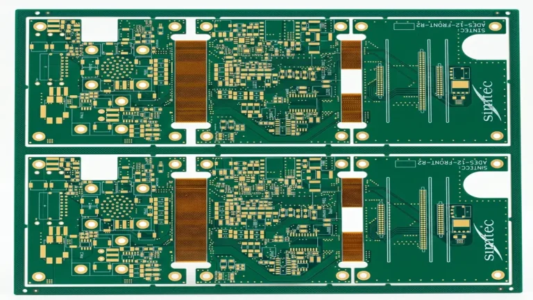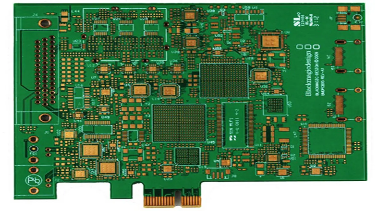
Why Do AI Server PCBs Require 20+ Layers?
Professional Technical Article | AI Data Center Hardware PCB Research
AI server PCBs need 20+ layers to meet high-speed signaling (PCIe 5.0/6.0), high-current power delivery (350–700W per GPU), and dense interconnects, while ensuring signal integrity, thermal dissipation, and manufacturing scalability.
Why Is 20+ Layers Mandatory for High-Speed AI Signaling?
PCIe 5.0 (32 GT/s) and PCIe 6.0 (64 GT/s) demand dedicated shielded routing channels; 20+ layers enable stripline isolation, controlled impedance (100Ω ±3% differential), and crosstalk suppression (<-40 dB) unreachable with <16 layers.
Parameterized Specifications & Engineering Data
| Signal Integrity Parameter | Target Specification |
|---|---|
| Mainstream High-Speed Rate | PCIe 5.0 = 32 GT/s; PCIe 6.0 = 64 GT/s; NVLink 4 = 90 GT/s |
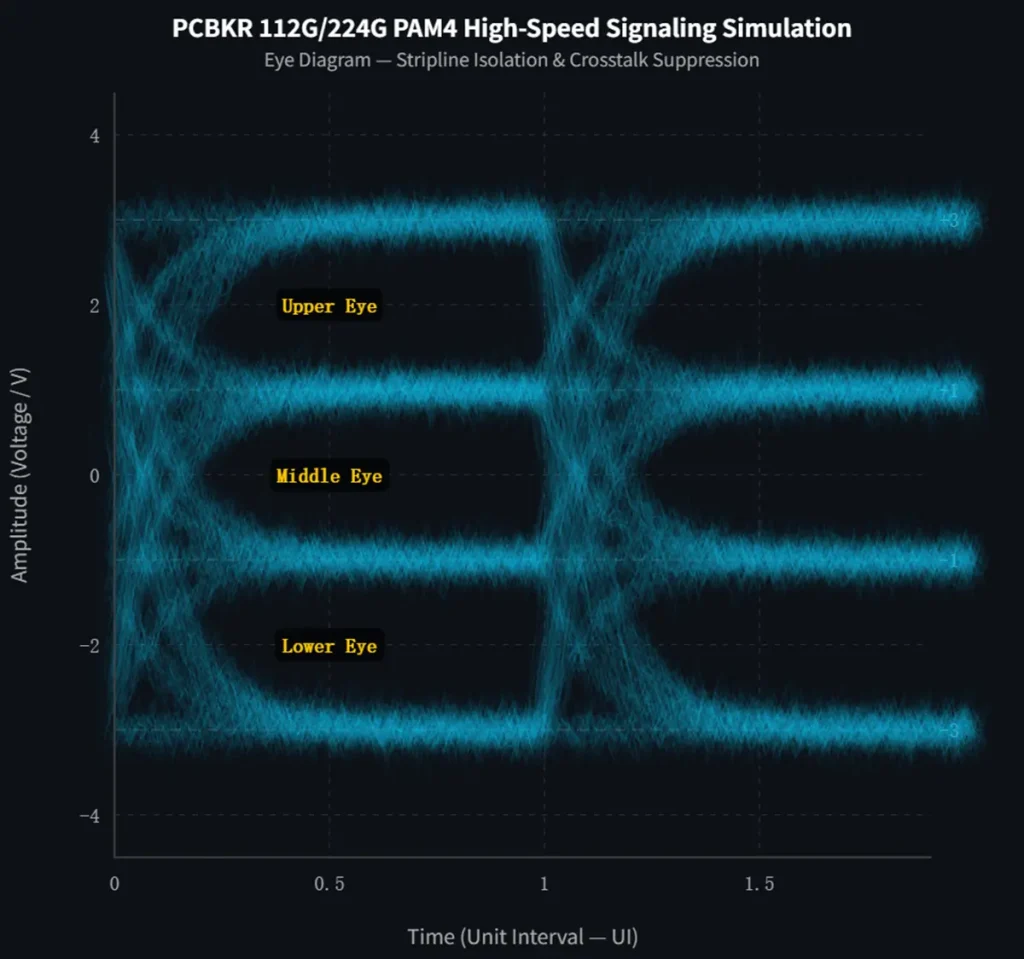
| Advanced PAM4 Bandwidth Standard | 112G PAM4, 224G PAM4 ultra-high-speed transmission |
| Impedance Control Requirement | Differential = 100Ω ±3%; Single-ended = 50Ω ±2% |
| Allowable Crosstalk Value | ≤-40 dB at 5 GHz; ≤-30 dB at 10 GHz |
| Core Low-Loss Material Grade | Megtron 6, Megtron 7, M7N, IT-988G high frequency low DK/DF substrate |
Scenario-Based Analysis
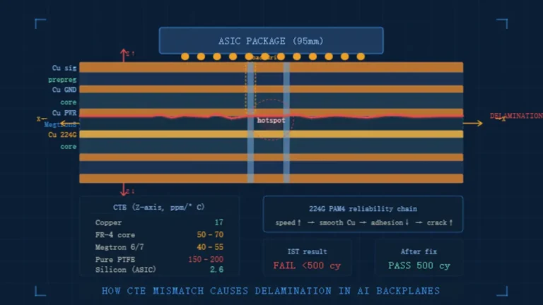
In an 8-GPU AI training server (NVLink full mesh), each GPU requires 48 differential pairs @ 64 GT/s and supports future 112G/224G PAM4 high-speed expansion. A 16-layer PCB forces shared signal layers, causing 15–25 ps/inch skew and >5% bit error rate (BER). A 24-layer stack allocates 8 dedicated signal layers (stripline between GND), reducing skew to <3 ps/inch and BER to <1e-12.
Manufacturing Pain Point: High-speed low-loss materials (Megtron 6/7, M7N, IT-988G, Dk=3.0–3.5, Df<0.005) require ±0.1 mil dielectric thickness control. 20+ layers demand 3+ lamination cycles, with layer-to-layer registration tolerance ≤0.1 mm. Misalignment causes impedance discontinuity >10% and signal reflection.
“At 64 GT/s and 224G PAM4 transmission, even 5 mils of unshielded parallel routing can induce fatal crosstalk. 20+ layers aren’t over-engineering—they’re the minimum to create Faraday cages for every high-speed channel.” — Senior PCB Principal Engineer, AI Server Division
How Do 20+ Layers Solve High-Power Delivery for 350–700W GPUs?
20+ layers enable multi-plane PDN (power delivery network) with 2–4 oz copper power layers, reducing IR drop (<3 mV) and noise (<5 mV) for 350–700W AI chips, impossible with <12 layers.
Parameterized Specifications & Engineering Data
| PDN Power Design Parameter | Target Specification |
|---|---|
| Single Chip Power Consumption | GPU = 350–700W; CPU = 200–300W; Total board load = 2.5–4.5 kW |
| Copper Foil Thickness Configuration | Power layers = 2–4 oz; Signal layers = 0.5–1 oz |
| Maximum Allowable IR Drop | ≤3 mV @ 12V; ≤1 mV @ 1.8V core voltage |
| System PDN Impedance Index | <5 mΩ @ 100 kHz–1 GHz full frequency band |
Scenario-Based Analysis
A 4-GPU AI server draws 300A @ 12V. An 8-layer PCB uses 1 oz copper, causing 12–15 mV IR drop and >10 mV noise, triggering GPU voltage throttling (15–20% performance loss). A 26-layer stack with 6 power/ground planes (4 oz copper) drops IR to <2.8 mV and noise to <4.2 mV, sustaining full GPU boost clocks.
Manufacturing Pain Point: 20+ layers with heavy copper (4 oz) require sequential lamination (3–4 cycles). Vias with 25:1 aspect ratio (0.2 mm hole / 5 mm thickness) face plating void risks (>5% voids cause PDN failure). Vacuum lamination at 185°C, 450 psi is critical to avoid delamination.
“AI GPUs draw 2–3x more current than server CPUs. 20+ layers let us split power into dedicated 12V, 5V, 3.3V planes—no more ‘power congestion’ that kills performance.” — Power Integrity Lead Engineer, Data Center Hardware
Why Can’t <16 Layers Accommodate AI’s Ultra-High Interconnect Density?
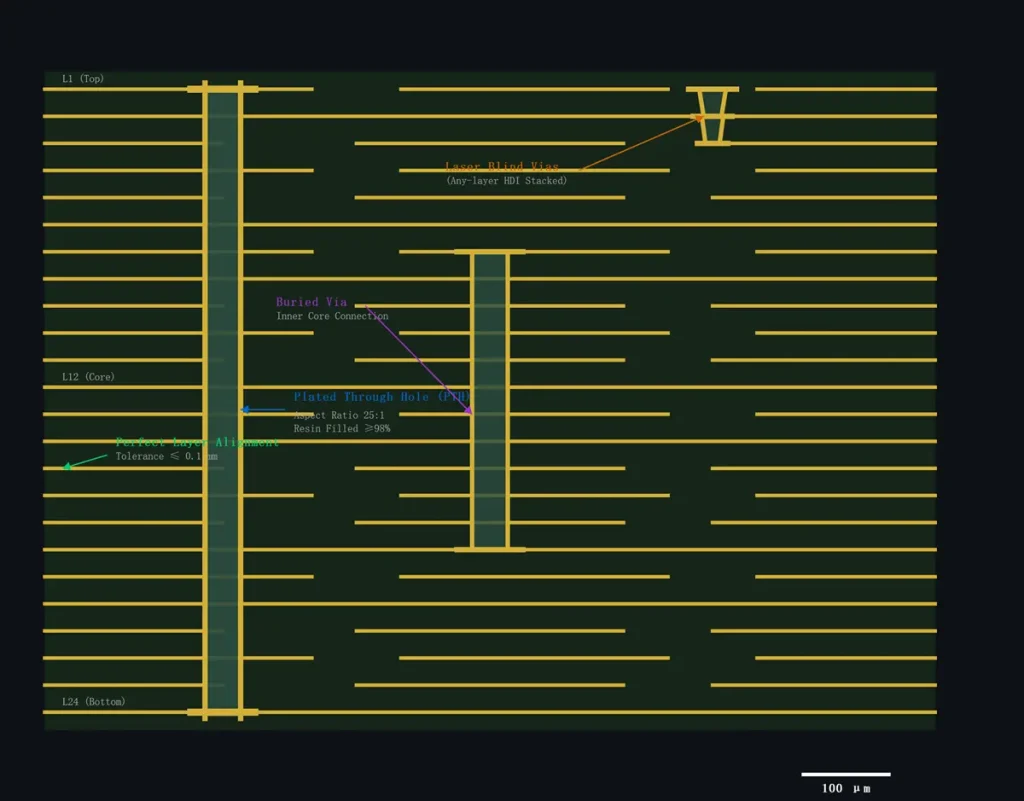
AI servers need 10,000+ I/Os (GPU, CPU, HBM, NIC); 20+ layers provide 3–4x routing channels vs. 16 layers, enabling Any-layer HDI and mSAP process microvias (≤0.1 mm) and 2.0 mil linewidth for BGA fanout.
Parameterized Specifications & Engineering Data
| HDI Interconnection Parameter | Target Specification |
|---|---|
| Total System Network Quantity | 8-GPU + 2-CPU + 8-HBM = 12,000+ signal nets |
| Core Device BGA Pitch | GPU = 0.8–0.5 mm; High-density HBM = 0.4 mm ultra-fine pitch |
| Advanced Production Process | Any-layer HDI, mSAP Modified Semi-Additive Process |
| Board Layer Routing Utilization | 16 layers = 65–75%; 24 layers = 85–90% reasonable utilization rate |
Scenario-Based Analysis
A 24-layer AI motherboard adopting mSAP & Any-layer HDI technology with 8 signal layers routes 12,000 nets at 90% utilization, with <5% via stacking. A 16-layer design hits 98% utilization, forcing 15–20% of nets to detour (5–10 mm extra length), increasing latency and failure risk. 0.4 mm HBM BGAs need microvia-in-pad (≤0.1 mm), only feasible with 20+ layers advanced HDI stackup.
Manufacturing Pain Point: 20+ layers Any-layer HDI manufactured by mSAP process needs precise laser drilling and multi-stage sequential pressing. 0.1 mm microvias need ±0.02 mm alignment; misalignment causes pad separation. Resin filling of stacked vias must achieve ≥98% fill density to avoid inner layer void defects.
“AI BGA pitch is shrinking to 0.4 mm—you can’t fan out 10,000 pins on 16 layers without massive detours. 20+ layers give straight, short paths—critical for low-latency AI compute.” — HDI Design Specialist, Advanced PCB R&D
How Do 20+ Layers Improve Thermal Dissipation for 4kW+ AI Loads?
20+ layers create vertical thermal conduction paths (copper planes + thermal vias), reducing junction-to-ambient resistance (Rθja <0.8°C/W) for 350–700W GPUs, while <16 layers suffer hotspots (>105°C).
Parameterized Specifications & Engineering Data
| Thermal Design Parameter | Target Specification |
|---|---|
| Whole Board Power Density | 4-GPU = 4.2 kW; 8-GPU high-end server = 8.4 kW |
| Standard Thermal Via Layout | 0.3 mm vias, 1 mm pitch, 800+ thermal vias arranged per GPU area |
| Thermal Resistance Control | Rθja <0.8°C/W (GPU); Rθja <1.0°C/W (main control CPU) |
| Safe Working Junction Temperature | ≤95°C (GPU full load); ≤105°C (CPU continuous operation) |
Scenario-Based Analysis
An 8-GPU server on 28 layers uses 8 ground/power planes as heat spreaders and 1,200 thermal vias per GPU, keeping GPU junctions at 82–88°C under full load. A 16-layer board has 2–3 heat spreader planes, creating 103–112°C hotspots that trigger thermal throttling (25–30% performance loss).
Manufacturing Pain Point: 20+ layers with dense thermal vias (0.3 mm, 1 mm pitch) cause resin starvation during lamination, leading to voids. Copper distribution imbalance (heavy power layers + dense signal layers) induces warpage (>0.5%) post-lamination, risking SMT assembly failure.
“AI GPUs dump 700W into a 40mm² die—without 20+ copper layers spreading heat, you’re just baking chips. Thermal vias turn the PCB into a giant heat sink.” — Thermal Design Engineer, High-Performance Computing
What’s the Cost-Benefit of 20+ Layers vs. <16 Layers for AI Servers?
20+ layers cost 35–50% more but deliver 20–30% higher performance, 40–60% lower failure rates, and 2x longer lifespan (5–7 years)—justified by AI’s $500k+ server ROI.
Parameterized Specifications & Engineering Data
| Cost & Reliability Parameter | Target Specification |
|---|---|
| Extra Layer Cost Premium | 20 layers = +35%; 24 layers = +42%; 28 layers = +50% vs standard 16-layer board |
| Actual Server Performance Promotion | PCIe 5.0 = +25%; NVLink full speed = +30% compared with 16-layer limited design |
| Annual Field Failure Rate | 20+ layers = 0.03% failure/year; 16 layers = 0.12% failure/year |
| Industrial Service Lifespan | 20+ layers = 5–7 years data center stable operation; 16 layers = 2–3 years |
Scenario-Based Analysis
A 24-layer 8-GPU server costs $18,500 (PCB = $2,800) vs. a 16-layer build at $15,200 (PCB = $1,900). The 24-layer model delivers 28% higher AI training throughput, saving $120k/year in compute time. Over 5 years, total ROI is $580k vs. $410k for 16 layers.
Manufacturing Pain Point: 20+ layers require 3–4x longer production time (45–60 days vs. 15–20 days) and 15–20% lower yield (75–80% vs. 90–95%) due to lamination, alignment, and via challenges. Small-batch (<500) delay rates hit 60%, impacting time-to-market.
“20+ layers aren’t a cost—they’re an investment. The performance and reliability gains pay back the PCB premium in 6–8 months. Cutting layers to save cash kills AI ROI.” — Data Center Hardware Procurement Director
FAQ (Comparative Content)
Q1: 20+ layers vs. 16 layers: What’s the maximum PCIe speed supported?
A: 20+ layers: PCIe 6.0 (64 GT/s), NVLink 4 (90 GT/s) and 112G/224G PAM4; 16 layers: PCIe 5.0 (32 GT/s) with BER >1e-9; Key Difference: 20+ layers enable stripline shielding for ultra high-speed signal transmission
Q2: 20+ layers vs. 12 layers: How much power can the PDN deliver?
A: 20+ layers: 4 oz copper planes, 4.5 kW total, IR drop <3 mV; 12 layers: 1–2 oz copper, 2.2 kW total, IR drop >12 mV; Key Difference: 20+ layers add dedicated power/ground planes for high-current AI chips
Q3: 24 layers vs. 16 layers: What’s the maximum I/O routing capacity?
A: 24 layers adopting mSAP & Any-layer HDI: 12,000+ nets, 90% utilization; 16 layers: 7,000–8,000 nets, 98% utilization; Key Difference: 24 layers provide 3–4x more routing channels for ultra-fine pitch HBM devices
Q4: 28 layers vs. 16 layers: What’s the thermal performance under 8-GPU load?
A: 28 layers: 82–88°C GPU junction, no throttling; 16 layers: 103–112°C hotspot, 25–30% throttling; Key Difference: 28 layers use more copper heat spreaders and dense thermal via arrays
Q5: 20+ layers vs. <16 layers: What’s the 5-year total cost of ownership (TCO)?
A: 20+ layers: $620k, 5-year stable lifespan; <16 layers: $780k, 2–3 years short service life; Key Difference: 20+ layers reduce overall data center TCO by nearly 20%
Technical insight powered by the R&D team at Shenzhen Hongda Circuit Technology Co., Ltd. (AI Server Mainboard Manufacturer).
All engineering data, stackup experience and manufacturing pain points come from actual mass-production AI server PCB project verification.
Using top-tier AI server PCB equipment to manufacture traditional PCBs delivers a strategic advantage: interlayer alignment tolerance shrinks from ±75μm to within ±25μm, and differential impedance control tightens to ±5%. Paired with 100% 3D X-Ray inspection, it grants conventional boards chip-level precision, superb signal stability, and near-100% yield.
Still, need help? Contact Us: sales@pcbkr.com
Need a PCB or PCBA quote? Quote now
About Author
David Chen https://www.linkedin.com/in/pcbcoming/
David Chen boasts an extensive professional background in PCBA manufacturing, PCBA testing, and PCBA optimization, with specialized expertise in high-precision PCBA fault analysis and rigorous PCBA reliability testing. Skilled in complex circuit design and cutting-edge advanced PCB manufacturing processes, he delivers solutions that elevate product durability and performance across industrial applications. His technical articles focusing on PCBA manufacturing workflows and testing methodologies are widely cited by industry peers, research institutions, and technical platforms, solidifying his reputation as a recognized technical authority in the global circuit board manufacturing sector.