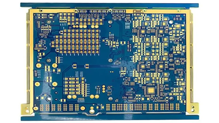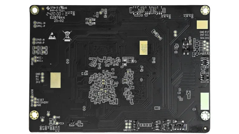
How Can You Get a Fast PCB Prototype Within a Realistic 24–48-Hour Production Window?
A fast PCB prototype depends on more than a manufacturer’s advertised turnaround time. Design readiness, material availability, layer count, engineering review, production scheduling, and inspection all affect the actual lead time. PCBKR has documented an anonymized 10-piece PCB order that was completed and inspected within approximately 24.5 hours after engineering confirmation, then shipped 25 hours and 31 minutes after confirmation. This is a specific production record, not a universal 24-hour guarantee. For a project review, contact sales@pcbkr.com.
1. What Determines Whether a PCB Prototype Can Be Manufactured Quickly?
A short PCB fabrication window is achievable only when the design, materials, and production requirements are compatible with the available manufacturing schedule.
The main factors are:
| Factor | What affects lead time | What buyers should prepare |
|---|---|---|
| Layer count | More layers generally require additional lamination and process steps | Final layer count and stackup |
| PCB material | Standard FR-4 and specialized materials may have different availability | Exact material grade or approved equivalent |
| Board thickness | Non-standard thicknesses may require process adjustment | Finished board thickness and tolerance |
| Copper weight | Heavy copper can require different etching and plating controls | Finished copper weight by layer |
| Minimum features | Fine lines, small holes, and tight registration can increase process complexity | Minimum trace/space, hole sizes, and tolerances |
| Surface finish | Different finishes have different process and scheduling requirements | ENIG, HASL, OSP, or another specified finish |
| Engineering data | Missing or inconsistent files can delay CAM review | Complete Gerber, drill, stackup, and fabrication notes |
| Inspection requirements | Additional tests or documentation can extend the completion schedule | Electrical test, impedance, and inspection requirements |
A two-layer standard FR-4 prototype and a multilayer HDI prototype should not be assigned the same assumed lead time. The manufacturing route must be reviewed against the actual design.
2. Which PCB Prototypes Are More Suitable for Quick-Turn Manufacturing?
The simplest way to improve prototype lead time is to avoid unnecessary manufacturing complexity while preserving the electrical and mechanical requirements of the design.
Standard FR-4 prototypes
A standard FR-4 PCB may be a suitable candidate for a short production window when:
- The layer count and board thickness are within the factory’s available process range.
- The material is available for the required production schedule.
- The Gerber and drill files are complete and consistent.
- The design does not require unusual hole, copper, or registration specifications.
- The inspection requirements can be completed within the requested schedule.
Multilayer PCB prototypes
Multilayer boards require additional consideration because inner-layer imaging, lamination, drilling, plating, and registration all contribute to the production route.
Before requesting a rapid turnaround, provide the complete stackup and confirm:
- Total layer count.
- Core and prepreg construction.
- Finished board thickness.
- Copper weight for each layer.
- Controlled impedance requirements.
- Blind, buried, or stacked via structures, if applicable.
For projects involving HDI structures, review the manufacturing requirements through PCBKR’s HDI PCB manufacturing page.
Specialized-material prototypes
High-frequency, high-speed, and other specialized-material boards may need additional engineering review. Material availability, bonding systems, surface treatment, and the specified electrical performance can affect the production schedule.
Do not assume that a standard FR-4 turnaround applies to a design using a specialized laminate.
3. How Can DFM Review Prevent PCB Prototype Delays?
Engineering review should take place before the production schedule is confirmed. A fast quotation does not necessarily mean the design is ready for manufacturing.
Common issues that can delay a prototype include:
- Gerber files that do not match the drill files.
- Missing or inconsistent board thickness information.
- Unclear copper weight specifications.
- Annular ring or hole-size requirements outside the proposed process capability.
- Incomplete stackup information.
- Unconfirmed impedance requirements.
- Unclear solder mask, legend, or surface finish specifications.
- Missing fabrication notes or conflicting revision information.
For time-sensitive orders, submit the final design package rather than an incomplete preliminary version.
If engineering identifies a manufacturability issue, the buyer and manufacturer should agree on the correction before production release. Starting production with unresolved specifications can create a larger delay later.
4. How Do Material Availability and Production Scheduling Affect Lead Time?
A design may be technically manufacturable but still unsuitable for a requested production window if the required material or process capacity is unavailable.
Before confirming a quick-turn schedule, the manufacturer should review:
- Material availability: Is the specified laminate available in the required thickness and copper construction?
- Production route: How many imaging, lamination, drilling, plating, and finishing steps are required?
- Process compatibility: Can the requested design be manufactured using an available qualified process?
- Production capacity: Can the order enter production within the requested time?
- Inspection requirements: Can the required inspection and electrical testing be completed before dispatch?
A realistic schedule should be confirmed after these checks, not inferred from a general turnaround-time statement.
5. What Information Should You Include in a Fast PCB Prototype RFQ?
A complete RFQ helps the manufacturer assess manufacturability and provide a more reliable lead-time estimate.
| RFQ item | Information to provide |
|---|---|
| Gerber files | Final fabrication data |
| Drill files | NC drill data and plated/non-plated hole information |
| Layer count | 2-layer, 4-layer, multilayer, or HDI |
| Material | FR-4 grade or specified specialty laminate |
| Finished thickness | Nominal thickness and tolerance |
| Copper weight | Required copper weight by layer |
| Board dimensions | Length, width, and panelization requirements |
| Quantity | Prototype quantity, including any spare-board requirement |
| Surface finish | ENIG, HASL, OSP, or specified alternative |
| Electrical requirements | Impedance, netlist, or other applicable requirements |
| Inspection | Electrical test and any additional inspection requirements |
| Delivery | Required dispatch date and destination |
For a turnkey PCB assembly request, also provide the BOM, centroid/pick-and-place data, assembly drawings, component sourcing requirements, and testing instructions.
A clear distinction between PCB fabrication and PCBA assembly is important. The completion time for bare boards does not automatically include component sourcing, SMT assembly, functional testing, or final system integration.
6. What Does a Real 24-Hour PCB Manufacturing Record Show?
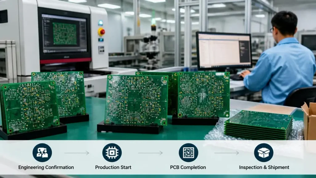
A documented PCB prototype production timeline showing manufacturing completion, inspection, and shipment milestones.
A real production record is more useful than an unrestricted quick-turn marketing claim. It should show when engineering confirmation occurred, when production started, when PCB fabrication was completed, when inspection finished, and when the order was dispatched.
The following anonymized record was provided by PCBKR.
Anonymized PCB prototype production record
<text>Order reference: Anonymized</text>
| Production milestone | Recorded time |
|---|---|
| Engineering confirmation | November 10, 08:00 |
| Formal production start | November 10, 08:20 |
| PCB manufacturing completion | November 11, 08:20 |
| Inspection completion | November 11, 08:30 |
| Shipment dispatch | November 11, 09:31 |
Order quantity: 10 PCS
PCB structure: Not disclosed in this published record.
Material and finished thickness: Not disclosed in this published record.
Calculated production intervals
| Measurement | Elapsed time |
|---|---|
| Engineering confirmation to production start | 20 minutes |
| Formal production start to PCB completion | 24 hours |
| PCB completion to inspection completion | 10 minutes |
| Inspection completion to shipment dispatch | 1 hour 1 minute |
| Engineering confirmation to inspection completion | 24 hours 30 minutes |
| Engineering confirmation to shipment dispatch | 25 hours 31 minutes |
This record demonstrates that one 10-piece PCB order entered formal production 20 minutes after engineering confirmation, reached PCB manufacturing completion 24 hours after production started, passed the recorded inspection milestone 10 minutes later, and was dispatched 25 hours and 31 minutes after engineering confirmation.
The record does not establish that every PCB design can be manufactured within 24 hours. It also does not establish the customer’s delivery time. Shipment dispatch and arrival at the customer’s location are different milestones.
The board structure, material, and thickness have not been disclosed in this case summary. They should not be assumed to be standard FR-4, two-layer, or any other particular construction.
What this production record does and does not prove
It supports a specific, traceable production timeline for one anonymized order. It does not establish a guaranteed lead time for other layer counts, materials, quantities, or manufacturing requirements.
For a published case study, the underlying production record should be retained so that the timestamps and order details can be verified. If additional order records become available, they can help establish whether similar turnaround times are repeatable for comparable PCB constructions.
7. How Does PCBKR Support Fast PCB Prototype Manufacturing?
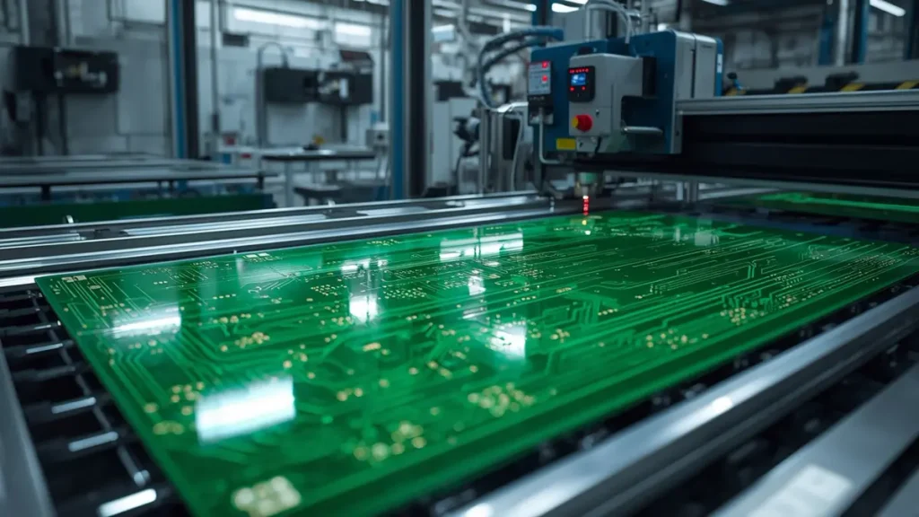
PCBKR uses specialized PCB fabrication equipment and inspection processes to support prototype and quick-turn manufacturing requirements.
PCBKR provides PCB fabrication and PCBA manufacturing services for prototype, small-batch, and production requirements.
The manufacturing process can involve different equipment and inspection methods according to the board construction and customer specifications.
Relevant manufacturing resources include:
- Laser Direct Imaging (LDI): Used for circuit imaging, with process capability evaluated against the actual design requirements.
- Lamination equipment: Supports multilayer PCB manufacturing using process parameters selected for the material and stackup.
- UV and CO₂ laser drilling: Supports laser-drilled structures according to the qualified manufacturing process.
- AOI and X-ray inspection: Applied where appropriate to inspect circuit features and internal structures.
- Electrical testing: Flying probe and other applicable test methods can be selected according to the order requirements.
- Impedance verification: Available for projects requiring controlled-impedance manufacturing and verification.
Equipment specifications alone do not establish the achievable lead time for an individual order. The actual schedule depends on design complexity, material availability, production capacity, and the required inspection plan.
For HDI and fine-feature projects, engineering review is particularly important. See the PCB microvia and mSAP manufacturing guide for related manufacturing considerations.
8. How Can Buyers Reduce the Risk of Missing a Prototype Deadline?
Buyers can reduce avoidable delays by preparing the following information before requesting a quick-turn quote:
- Send the final Gerber, drill, and fabrication files.
- Confirm the layer count, material, copper weight, and finished thickness.
- Identify any controlled-impedance or special tolerance requirements.
- Confirm whether the order is PCB fabrication only or includes PCBA assembly.
- Provide the required quantity and inspection specifications.
- Identify the required shipment date and destination.
- Confirm that engineering questions and file revisions can be answered promptly.
If a design changes after production release, the manufacturer may need to repeat engineering review or adjust the production schedule. The buyer should therefore confirm the revision before authorizing production.
9. Request a Fast PCB Prototype Quote from PCBKR
If you need a fast PCB prototype, send your Gerber files, drill files, stackup, quantity, material requirements, and target shipment date to PCBKR.
Our engineering and production teams can review the design, identify manufacturing constraints, and assess whether the requested turnaround is feasible.
Contact: sales@pcbkr.com
Website: https://www.pcbkr.com/
A realistic lead time should be confirmed after reviewing the actual design and production requirements. Selected projects may qualify for a short manufacturing window, but a 24–48-hour schedule should never be treated as an unconditional promise.
Frequently Asked Questions
Can a PCB prototype really be manufactured within 24 hours?
Some selected PCB orders may be completed within a 24-hour manufacturing window after formal production release. Feasibility depends on the design, material availability, layer count, production capacity, and inspection requirements. PCBKR’s documented 10-piece order in this article reached PCB manufacturing completion 24 hours after formal production started.
Does a 24-hour PCB manufacturing time include shipping?
No. PCB manufacturing completion, inspection completion, shipment dispatch, and customer delivery are separate milestones. The anonymized order in this article was dispatched 25 hours and 31 minutes after engineering confirmation. The record does not state the customer’s delivery time.
Which files are required for a fast PCB prototype quotation?
At minimum, provide the final Gerber files, NC drill files, layer count, material, finished thickness, copper weight, quantity, surface finish, and required tolerances. Include stackup and impedance information when applicable.
Are multilayer and HDI prototypes eligible for quick-turn production?
They may be, depending on the design and available production schedule. Multilayer and HDI structures can require additional lamination, drilling, registration, and inspection steps. The manufacturer must review the actual stackup and via structure before confirming the lead time.
How can I confirm whether my PCB order qualifies for a 24–48-hour production window?
Send your complete manufacturing files, material specifications, quantity, and target date to PCBKR. The engineering team can review the design and production requirements before confirming a feasible schedule. A short turnaround should only be promised when the specific order has been reviewed and accepted for production.
About the Author
David Chen LinkedIn Profile
David Chen is a Senior RF/PCB Process Engineer at Shenzhen Hongda Circuit Technology Co., Ltd., with over 12 years of experience in high-frequency PCB fabrication, impedance-controlled stack-up design, and Rogers/PTFE laminate processing. He also boasts an extensive professional background in PCBA manufacturing, PCBA testing, and PCBA optimization, with specialized expertise in high-precision PCBA fault analysis and rigorous PCBA reliability testing. The author has worked with high-layer-count server PCB fabrication, ultra-low-loss backplane stackups, and thermo-mechanical reliability optimization for AI infrastructure projects involving 112G and 224G PAM4 architectures. Skilled in complex circuit design and cutting-edge advanced PCB manufacturing processes, he delivers solutions that elevate product durability and performance across industrial applications. His technical articles focusing on PCBA manufacturing workflows and testing methodologies are widely cited by industry peers and technical platforms, and have gained attention and recognition from industry colleagues.