Why Are AI Server PCBs Harder to Manufacture?
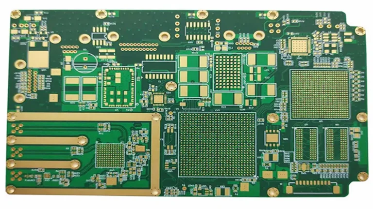
AI server PCBs are harder to manufacture because they simultaneously demand ultra-high layers (20–36+), 112G/224G PAM4 signaling, massive 1000A+ current delivery, and micron-level tolerances. Achieving this forces manufacturers to mix ultra-low-loss materials and heavy copper, where any microscopic fabrication deviation triggers immediate signal collapse or catastrophic thermal runaway.
Why Do AI Server PCBs Require Much Tighter Manufacturing Tolerances?
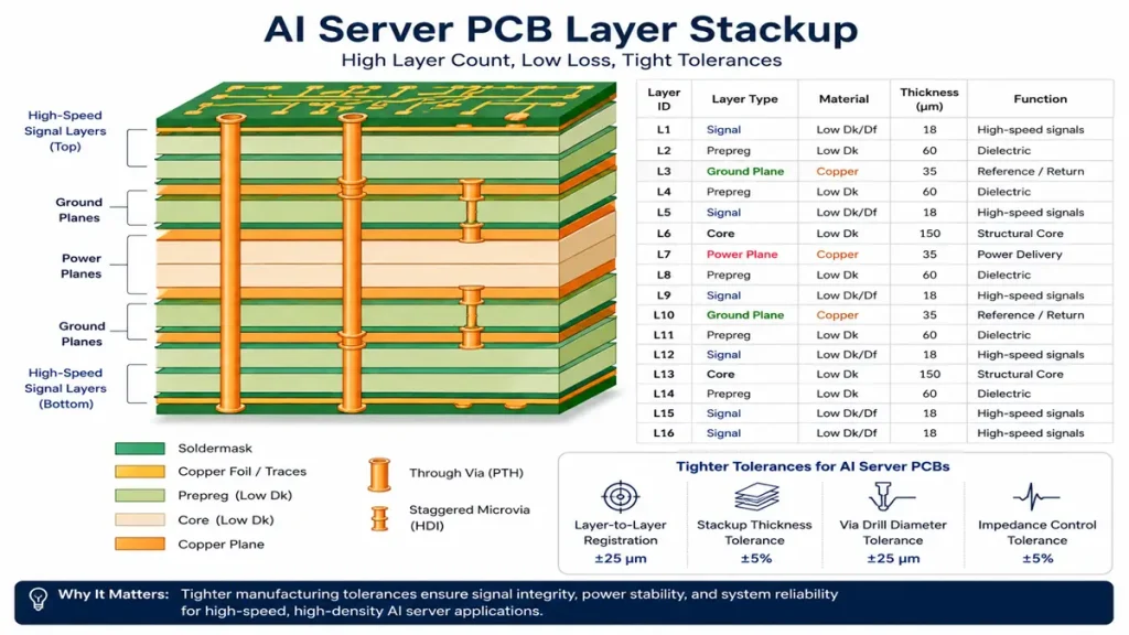
AI Server PCB Layer Stackup
Direct Answer: Modern AI server PCBs operate at extremely high signaling speeds where tiny fabrication deviations directly affect insertion loss, impedance stability, and timing margins.
| Parameter | Traditional Server PCB | AI Server PCB |
|---|---|---|
| Layer Count | 8–16 Layers | 20–36 Layers |
| Impedance Tolerance | ±10% | ±3% to ±5% |
| Trace Width Tolerance | ±15 μm | ±5–7 μm |
| Backdrill Stub | <10 mil | <4 mil |
| Surface Roughness | 3–5 μm | <1 μm |
Manufacturing Pain Point:
At 112G PAM4, using a typical 100Ω differential pair structure with approximately 3.5 mil dielectric thickness and ultra-low-loss material, a copper over-etch of only 8 μm can shift differential impedance by roughly 4–6 Ω. This is sufficient to reduce eye opening margins and trigger GPU communication instability during high-speed SerDes operation.
Why Does Layer Registration Become a Major Manufacturing Bottleneck?
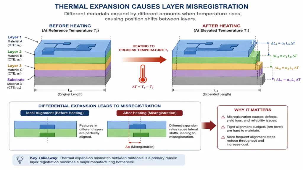
Schematic Diagram of Thermal Expansion
Direct Answer: AI server PCBs use large panel sizes and multiple sequential lamination cycles. Differential thermal expansion causes cumulative registration drift between layers.
Typical AI accelerator motherboard specifications:
- 28–36 layers
- 2.8–4.5 mm board thickness
- 610 × 650 mm panel size
- 3 sequential lamination cycles
Real Engineering Scenario:
One 28-layer AI GPU motherboard showed 18 μm layer offset at the center but 61 μm drift near the edge after lamination. The PCB passed AOI but failed 112G channel margin validation because timing skew exceeded SerDes compensation capability.
Expert Engineering Insight on Sequential Lamination:
When managing three sequential lamination cycles on a 610 × 650 mm oversized panel, the material core shrinkage (X/Y axis dimensional coefficient) becomes highly non-linear. In advanced AI PCB cleanrooms, standard pin-lamination processes often fail. Manufacturers increasingly rely on Inductive Heating Bond systems combined with X-ray target compensation to dynamically adjust for Megtron 7 resin flow behavior. Without compensating for cumulative thermal shrinkage inside ultra-low-loss laminates, inner-layer annular rings can breakout, creating hidden open-circuit risks that only appear later under sustained GPU thermal loading.
Why Is Backdrilling Much More Difficult in AI Server PCBs?
Direct Answer: AI server PCBs are much thicker than standard boards, making drill depth control and stub removal extremely difficult.
| Signal Speed | Required Residual Stub Length |
|---|---|
| 25G NRZ | <10 mil |
| 56G PAM4 | <6 mil |
| 112G PAM4 | <4 mil |
| 224G PAM4 (Target Specification) | <2 mil |
Detailed Manufacturing Pain Point:
A 3.8 mm AI switch backplane with an aspect ratio above 18:1 experienced drill wander exceeding 65 μm. Residual via stubs ranged from 3 mil to 11 mil, causing resonant peaks near 24–28 GHz and intermittent NCCL timeout failures during AI cluster training.
Why Does Copper Balance Become Extremely Difficult in AI Power Delivery Networks?
Direct Answer: AI accelerators consume enormous current, forcing PCB manufacturers to combine fine signal routing with extremely heavy copper power planes.
| Hardware | Typical Current |
|---|---|
| Traditional CPU Server | 80–150 A |
| AI GPU Module | 600–1000 A |
| AI Training Tray (System-Level Aggregate Current) | 4000–8000 A |
Expert Manufacturing Observation:
Copper density may vary from 15% to 90% across the same PCB panel. During lamination, thin-copper areas over-compress while heavy-copper zones under-compress, producing dielectric thickness variation and impedance instability.
Detailed Manufacturing Pain Point (Resin Starvation & Voids):
The stark contrast between 90% heavy copper zones for 1000A GPU rails and 15% fine-line signal routing creates severe resin starvation challenges. During pressing, standard prepregs cannot fully fill the large step transitions generated by 2oz/3oz copper structures. This leaves microscopic dielectric voids trapped inside the laminate. Under high-voltage AI operating conditions, these voids accelerate localized CAF (Conductive Anode Filament) growth, transforming a premium AI accelerator board into a long-term reliability risk. Under sustained high-temperature and high-humidity operating environments, these micro-void regions can accelerate localized CAF growth and potentially trigger premature insulation failure compared with traditional server platforms.
One real GPU power delivery failure involved:
- 900 A transient current
- 0.18 mΩ localized resistance deviation
- Localized hotspot above 160°C
- Via barrel fatigue cracking after repeated training cycles
Why Are Ultra-Low-Loss Materials Harder to Process?
Direct Answer: AI server PCBs increasingly rely on ultra-low-loss laminates that are mechanically harder to drill, laminate, and plate than standard FR-4.
| Material | Typical Drill Bit Life |
|---|---|
| Standard FR-4 | 2500 hits |
| Megtron 6 | 1400 hits |
| Megtron 7 | Below 500 to 900 hits depending on panel density, stackup complexity, and drilling parameters |
Manufacturing Challenge:
Low-loss materials have lower resin flow and higher rigidity. This increases drill wear, hole roughness, copper adhesion instability, and CAF risk under high thermal cycling environments.
Expert Metallurgical & Chemical Experience:
Processing ultra-low-loss PTFE or polyphenylene ether (PPE) laminates is extremely difficult for conventional PCB fabrication lines. Because these materials are chemically inert, standard permanganate desmear chemistry cannot create sufficient surface roughness for copper adhesion. Advanced AI PCB production increasingly relies on Plasma Etching using carefully controlled CF4/O2 gas ratios to nano-roughen the resin surface before electroless copper deposition. If the plasma activation cycle drifts by even 30 seconds, copper plating adhesion can fail during 288°C solder float testing, destroying the entire production lot.
Why Does Through-Hole Copper Uniformity Become a Critical AI PCB Challenge?
Direct Answer: AI server PCBs frequently use extremely high aspect-ratio vias above 16:1 or even 18:1, making uniform copper plating inside deep holes extraordinarily difficult.
| PCB Type | Typical Aspect Ratio |
|---|---|
| Consumer Electronics PCB | 6:1 to 8:1 |
| Telecom Backplane | 10:1 to 12:1 |
| AI Server PCB | 16:1 to 20:1 |
Critical Electroplating Bottleneck:
As PCB thickness increases, electroplating throwing power drops sharply. The top section of the via barrel may receive excessive copper deposition while the center section remains dangerously thin. In AI server boards carrying high transient current, insufficient center-barrel copper thickness dramatically increases thermal fatigue risk during continuous GPU loading.
Real Factory Reliability Scenario:
A 32-layer AI switch board with a 4.2 mm thickness and 0.20 mm mechanical drill diameter showed center-barrel copper thickness below 16 μm while surface copper exceeded 32 μm. The board passed initial continuity testing but later developed intermittent resistance drift after thermal shock cycling due to uneven copper stress distribution inside the via structure.
Why Is Thermal Reliability Much More Dangerous in AI Server PCBs?
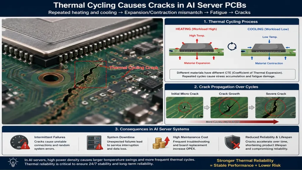
Thermal Cycling Cracking Diagram
Direct Answer: AI server PCBs operate under continuous high current and thermal stress, accelerating microvia fatigue and copper crack formation.
| Region | Typical Temperature |
|---|---|
| Standard VRM | 70–90°C |
| AI GPU VRM | 110–140°C |
| NVLink / SerDes Area | 95–120°C |
Failure Chain Example:
Repeated AI training cycles create continuous expansion and contraction inside stacked microvias. Crack initiation commonly occurs at staggered via knee regions, causing resistance drift from 0.4 mΩ to 3.8 mΩ before catastrophic open-circuit failure.
Why Do AI Server PCB Failures Often Appear Only During Real AI Training?
Direct Answer: Traditional electrical testing cannot fully simulate simultaneous high-speed signaling, transient current spikes, and continuous thermal cycling found in real AI clusters.
Real Deployment Failure:
An 8-GPU AI training server passed burn-in and ICT testing but failed after 9 days of continuous LLM training. Root cause analysis identified backdrill residual inconsistency combined with thermal-induced dielectric constant drift, causing intermittent PAM4 eye collapse.
FAQ
Why are AI server PCBs more expensive than traditional server PCBs?
Because they require ultra-low-loss materials, extremely tight tolerances, heavy copper structures, high layer counts, and much lower acceptable defect margins.
Why is 112G/224G PAM4 manufacturing so difficult?
At these frequencies, tiny physical deviations create major signal integrity problems including impedance drift, resonance, skew imbalance, and eye closure.
Why do AI server PCB failures appear weeks later?
Many failures are fatigue-driven rather than immediate defects. Thermal cycling and high current gradually damage vias and copper structures.
Why are stacked microvias risky in AI hardware?
Stacked microvias experience concentrated thermomechanical stress under repeated GPU power cycling, making them vulnerable to copper fatigue cracking.
Why are AI server PCB yields much lower?
Because AI boards combine multiple advanced technologies simultaneously: HDI, heavy copper, ultra-low-loss materials, high layer counts, and precision backdrilling.
Using top-tier AI server PCB equipment to manufacture traditional PCBs delivers a strategic advantage: interlayer alignment tolerance shrinks from ±75μm to within ±25μm, and differential impedance control tightens to ±5%. Paired with 100% 3D X-Ray inspection, it grants conventional boards chip-level precision, superb signal stability, and near-100% yield.
Still, need help? Contact Us: sales@pcbkr.com
Need a PCB or PCBA quote? Quote now
About Author
David Chen https://www.linkedin.com/in/pcbcoming/
David Chen boasts an extensive professional background in PCBA manufacturing, PCBA testing, and PCBA optimization, with specialized expertise in high-precision PCBA fault analysis and rigorous PCBA reliability testing. Skilled in complex circuit design and cutting-edge advanced PCB manufacturing processes, he delivers solutions that elevate product durability and performance across industrial applications. His technical articles focusing on PCBA manufacturing workflows and testing methodologies are widely cited by industry peers, research institutions, and technical platforms, solidifying his reputation as a recognized technical authority in the global circuit board manufacturing sector.