Gold Finger PCB Manufacturing Process: Technical Guide, Quality Standards & Advanced Fabrication Capabilities
Gold finger PCBs remain the backbone of high-reliability interconnection across server backplanes, PCIe expansion cards, industrial control modules, and telecommunications infrastructure. Yet procurement engineers and hardware designers consistently face the same field failures: premature gold wear at the contact edge, nickel barrier corrosion after 500+ insertion cycles, impedance drift caused by uneven plating thickness, and beveling burrs that damage mating connectors. These are not design flaws—they are manufacturing control gaps.
At Shenzhen Hongda Circuit Technology Co., Ltd., we have built our gold finger PCB manufacturing process around the principle that edge connector reliability is determined long before the board reaches your assembly line. Our production floor integrates pulse electroplating technology, automated nickel-barrier control, and real-time XRF thickness verification to deliver hard gold plated edge connectors that meet IPC-6012 Class 3, IPC-4556, and MIL-G-45204C requirements—whether you need 30 µin for standard PCI cards or 150 µin for military-grade backplane systems.
This blog breaks down the complete gold finger PCB fabrication workflow, the science behind cobalt-alloy hard gold plating, mandatory IPC quality gates, critical design rules, and common manufacturing defects & solutions to help hardware designers and procurement teams select reliable PCB suppliers.
Gold Finger PCB Technical Specifications & Design Rules: Material Science and IPC Standards
Hard Gold vs. ENIG: Why Edge Connectors Demand Electroplated Cobalt-Alloy Gold
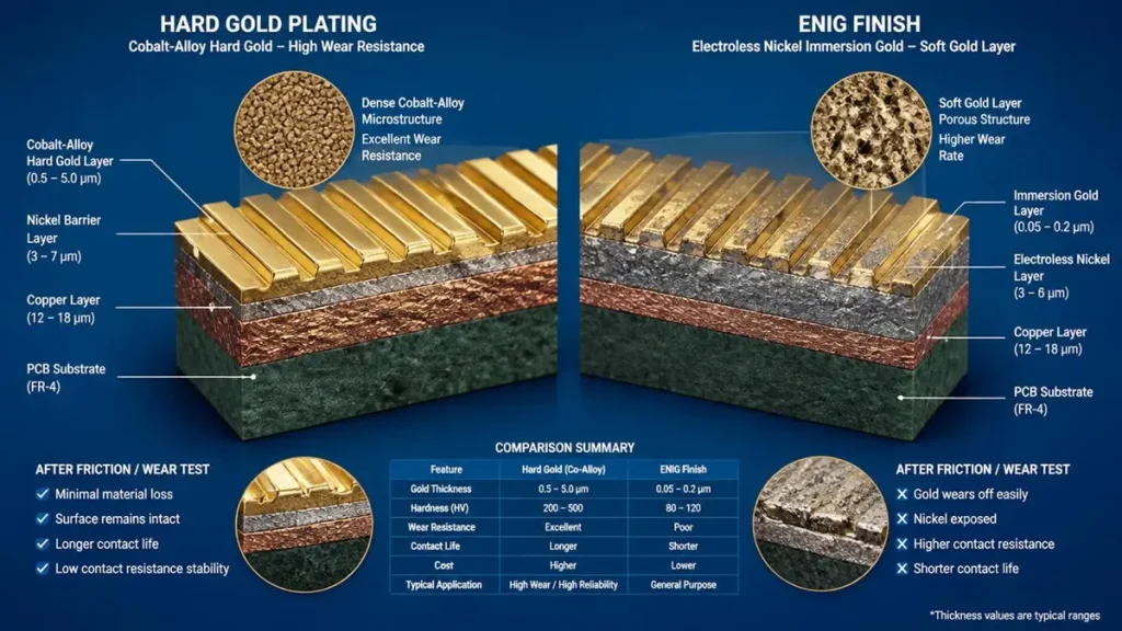
3D Microstructure & Cross-Section Analysis — Hard Gold Plating vs. ENIG Finish on PCB Gold Fingers
A recurring sourcing mistake is assuming all gold surface finishes deliver identical wear resistance. They do not. Electroless Nickel Immersion Gold (ENIG) deposits a soft gold layer—typically 2–5 µin thick with 99.9% purity—suitable for solderable SMD pads but entirely inadequate for repeated mechanical mating. Under friction, ENIG gold wears through in fewer than 50 cycles, exposing the nickel underneath to oxidation and creating intermittent contact resistance.
Hard gold plating for PCB gold fingers is an electrolytic process that deposits a gold-cobalt or gold-nickel alloy (98% Au, 2% Co/Ni). The cobalt additive increases Knoop hardness to 130–200 HK, transforming the deposit from a corrosion barrier into a wear-resistant mechanical surface. This is why IPC-4556 and IPC-6012F explicitly mandate electroplated hard gold for edge board contacts, not immersion gold.
| Surface Finish | Deposition Method | Hardness (HK) | Typical Thickness | Rated Insertion Cycles | Appropriate Use |
|---|---|---|---|---|---|
| ENIG (Soft Gold) | Chemical immersion | 60–90 | 2–5 µin | < 50 | Solder pads, non-mating areas |
| Electroplated Hard Gold (Cobalt) | Electrolytic | 130–200 | 30–50 µin | 1,000+ | Standard PCIe, graphics cards |
| Electroplated Hard Gold (Heavy) | Electrolytic | 130–200 | 50–150 µin | 10,000+ | Hot-swap servers, test fixtures |
At Hongda Circuit, our plating chemistry is maintained with automatic dosing systems that hold cobalt concentration within ±0.05%—a tolerance band tighter than industry average—to ensure consistent hardness across every production lot.
Nickel Barrier Layer: The Critical Diffusion Block Between Copper and Gold
Without an intermediate nickel layer, copper atoms migrate into the gold lattice within months, forming a brittle Cu-Au intermetallic that flakes under contact pressure. The nickel barrier serves three non-negotiable functions:
- Diffusion Inhibition: A dense nickel deposit (3–6 µm, or 120–240 µin) blocks copper migration at operating temperatures up to 125°C.
- Mechanical Support: Nickel provides a hard, smooth substrate that prevents gold from sinking into copper grain boundaries.
- Corrosion Resistance: The nickel layer itself acts as a sacrificial barrier if the gold coating is breached.
Our plating line utilizes pulse-reverse current technology for nickel deposition, which produces a finer grain structure (average grain size < 0.2 µm) compared to conventional DC plating. This microstructural refinement increases the barrier effectiveness by approximately 18% based on our cross-sectional analysis data.
Gold Thickness Specification by Application Class
Thickness is never arbitrary—it is a direct function of insertion cycle requirements and electrical load. The following matrix aligns IPC-6012F class designations with real-world gold finger thickness specifications:
| Application | IPC Class | Gold Thickness (µin) | Gold Thickness (µm) | Nickel Thickness (µin) | Expected Cycles |
|---|---|---|---|---|---|
| Consumer electronics, prototypes | Class 2 | 3–15 | 0.08–0.38 | ≥100 | 50–200 |
| General industrial, office equipment | Class 2 | 25–32 | 0.64–0.81 | ≥120 | 500–1,000 |
| Server motherboards, network cards | Class 2 | 30–50 | 0.76–1.27 | ≥150 | 1,000–5,000 |
| Telecom backplanes, medical devices | Class 3 | 50–100 | 1.27–2.54 | ≥150 | 5,000–10,000 |
| Aerospace, military avionics | Class 3 / 3A | 100–150 | 2.54–3.81 | ≥200 | 10,000+ |
Hongda Circuit maintains plating racks with dedicated auxiliary cathodes for each panel size, eliminating the “edge effect” that causes gold thickness to taper at the panel periphery. Our XRF mapping protocol measures nine points per finger array, ensuring no individual finger falls below the specified minimum.
Gold Finger Beveling Standards: 30°, 45°, and 60° Chamfer Geometry
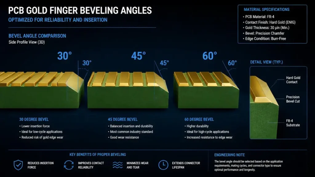
Precision CNC Beveling Geometry — 30°, 45°, and 60° Chamfer Angle Standards for PCB Gold Fingers
Beveling is not a cosmetic step. A properly chamfered edge reduces insertion force by 40–60% and prevents the sharp 90° corner from shearing the spring contacts inside the mating connector. Our CNC beveling machines support:
- 30° bevel: Standard for PCI, PCIe, and DIMM memory modules where shallow insertion angles are used.
- 45° bevel: Common for industrial backplane cards and hot-swap server trays requiring moderate ramp guidance.
- 60° bevel: Specialized for high-density connectors where board thickness exceeds 2.4 mm and aggressive tapering is needed.
Bevel depth is controlled to leave a residual edge thickness of 0.5 mm ±0.05 mm, verified by optical profile measurement after every tool change. We also perform segmented beveling for long-short finger designs used in hot-swap power sequencing.
Step-by-Step Gold Finger PCB Manufacturing Process at Hongda Circuit
Step 1: Base PCB Fabrication and Solder Mask Windowing
The process begins with standard multilayer fabrication through outer-layer etching. The critical difference for gold finger boards occurs at solder mask application: the mask must be pulled back from the edge connector lands by a minimum of 0.5 mm to prevent mask residue from contaminating the plating surface. Our LDI (Laser Direct Imaging) solder mask exposure system achieves registration accuracy of ±8 µm, ensuring clean mask edges that never encroach on the finger area.
For impedance-controlled gold finger designs—such as PCIe 5.0/6.0 edge connectors—we perform pre-layout simulation using Polar SI9000 to model the trace-to-finger transition. Copper pullback on internal layers is maintained at 3.0 mm from the board edge to prevent copper exposure during beveling.
Step 2: Selective Masking and Plating Bar Integration
Because electroplating requires electrical continuity, we integrate a temporary plating bar (tie-bar) along the panel edge. This bus connects all finger pads during current application and is mechanically routed off during final profiling. Our design rule check (DRC) software validates that no trace carries current through the plating bar after cut-off, eliminating latent short risks.
Blue polyester tape and liquid photoresist are applied to mask all non-finger areas. This selective plating approach reduces gold consumption by 60–70% compared to full-panel plating, a cost efficiency we pass directly to customers without compromising contact integrity.
Step 3: Pulse Electroplating of the Nickel Barrier
The masked panel enters our pulse-reverse nickel plating line. Unlike conventional DC plating, pulse-reverse current applies periodic anodic pulses that:
- Level surface micro-roughness, producing a mirror-like nickel surface (Ra < 0.1 µm);
- Reduce internal stress in the deposit, preventing nickel cracking under thermal cycling;
- Improve throwing power into high-aspect-ratio features adjacent to gold fingers.
Bath chemistry is monitored by an online titration system that samples nickel concentration, pH, and chloride levels every 15 minutes. If any parameter drifts outside the ±3% control limit, the system triggers automatic chemical addition and flags the lot for engineering review.
Step 4: Cobalt-Alloy Hard Gold Electroplating with Real-Time Thickness Control
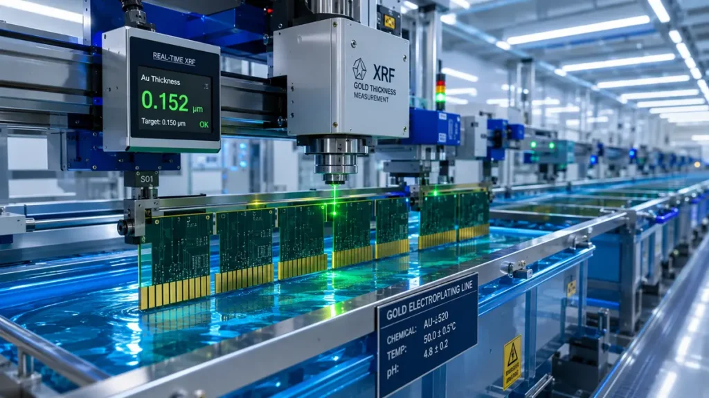
Automated Cobalt-Alloy Gold Electroplating Line with Real-Time XRF Thickness Verification and Bath Parameter Control
The core of gold finger reliability lies in this step. Our hard gold bath operates at 55°C with a proprietary cobalt sulfamate electrolyte. Panels are fixtured on titanium racks with conforming anodes that maintain a uniform current density of 2–4 A/dm² across the entire finger array.
Key process controls include:
- Current density mapping: Auxiliary cathodes at the panel corners balance current distribution, preventing the “dog-bone” thickness variation common in poorly fixtured plating.
- Bath agitation: Controlled air sparging eliminates hydrogen bubble pitting—a primary cause of surface porosity in gold deposits.
- Gold recovery: Rinse water passes through an ion-exchange gold recovery column, ensuring environmental compliance and recovering >98% of residual gold.
Plating time is calculated by Faraday’s law with a process-specific efficiency factor, then cross-checked against in-line micro-section samples. For a 50 µin target, typical deposition time is 22–28 minutes depending on panel loading.
Step 5: Precision CNC Beveling and Burr Control
After gold plating and solder mask curing, panels move to our fully automated CNC beveling station. The machine uses diamond-coated routing tools spinning at 40,000 RPM to chamfer the edge at the programmed angle. Critical controls include:
- Tool wear compensation: Automatic laser tool measurement checks cutting edge radius before each panel; tools are indexed when wear exceeds 5 µm.
- Vacuum fixturing: Eliminates panel vibration that causes micro-chipping of the gold edge.
- Burr detection: Post-bevel optical scanning identifies any burr > 25 µm; affected panels are re-routed or rejected.
For boards requiring long-short finger configurations—such as hot-swap server blades—we execute multiple bevel programs in a single fixturing, maintaining angular tolerance of ±1° across all finger segments.
Step 6: Plating Bar Cut-Off and Edge Profiling
The plating tie-bar is removed using a dedicated V-score and break process, followed by edge sanding to eliminate any residual copper sliver. For high-reliability Class 3 boards, we perform 100% electrical testing after bar removal to confirm no conductive path remains between previously connected fingers.
Step 7: Final Surface Finish for Non-Finger Areas
While gold fingers retain their hard gold finish, the remainder of the board receives its specified surface finish—ENIG, OSP, or HASL—through a separate process line. Strict process isolation prevents cross-contamination between the hard gold and immersion chemistry baths.
Gold Finger PCB Quality Control, Testing & Defect Prevention Protocols
Automated Optical Inspection (AOI) for Contact Surface Integrity
Our AOI system inspects every gold finger at 12 µm resolution, detecting:
- Solder mask encroachment onto the contact pad
- Surface pits, scratches, or foreign particle contamination
- Finger length and width deviations exceeding ±0.05 mm
- Missing plating or exposed nickel at the finger edge
Defect detection sensitivity is calibrated weekly using NIST-traceable reference standards. Any lot with a defect rate > 0.3% triggers a full root-cause analysis.
XRF Thickness Verification: Non-Destructive Gold and Nickel Measurement
X-ray fluorescence (XRF) is the industry-standard method for verifying plating thickness per IPC-4552 Rev B. Our protocol mandates:
- 100% first-article inspection: The first panel of every lot receives a 9-point XRF map (three points per finger across three representative fingers).
- Statistical sampling: Subsequent panels are sampled at AQL 0.65 (MIL-STD-105E General Level II).
- Guard banding: To account for XRF instrument uncertainty, we maintain a +10% process mean offset. A 30 µin specification is therefore plated to a 33 µin mean, ensuring no measurement falls below the minimum even under worst-case gauge error.
Our XRF instruments are calibrated quarterly against certified reference materials traceable to NIST, with inter-lab correlation studies conducted annually.
Electrical Testing: Flying Probe and Impedance Validation
After plating bar removal, every gold finger board undergoes:
- 100% flying probe testing: Open/short verification between all fingers and the internal circuit, ensuring no plating bar residue creates latent shorts.
- Controlled impedance testing (TDR): For high-speed designs, test coupons embedded in the production panel are measured by time-domain reflectometry to confirm impedance within ±5% of target.
- Contact resistance sampling: Four-point probe measurements verify that finger-to-finger resistance variation does not exceed 5 mΩ.
Adhesion and Mechanical Reliability Testing
- Tape adhesion test (per IPC-TM-650 2.4.28.1): 3M 600 tape is applied and peeled at 180°; any gold flaking constitutes rejection.
- Cross-hatch test: A 1 mm grid is scribed through the gold to the nickel; adhesion is rated per ASTM D3359.
- Insertion cycle simulation: Sample boards are mated and unmated in a mechanical fixture for 1,000 cycles (or customer-specified count), followed by XRF re-measurement to verify gold retention > 80% of initial thickness.
Common Gold Finger PCB Manufacturing Defects and Hongda Circuit Prevention Methods
Defect 1: Gold Finger Pitting and Surface Porosity
Root cause: Hydrogen bubble adhesion during plating or organic contamination in the gold bath.
Prevention: Our plating tanks employ programmable air sparging cycles that dislodge bubbles before they stabilize on the cathode. Bath organic contamination is controlled through continuous carbon filtration and weekly TOC (total organic carbon) analysis. When TOC exceeds 15 ppm, the bath is treated with activated carbon and re-certified before production resumes.
Defect 2: Uneven Gold Thickness Distribution
Root cause: Non-uniform current density due to poor rack design or panel positioning.
Prevention: Hongda Circuit uses rack-specific auxiliary anodes for each panel dimension (standard, oversized, and long-format server boards). Current distribution is modeled using finite element analysis during rack design, then validated by XRF mapping across a 25-point grid before the rack is approved for production.
Defect 3: Beveling Burrs and Edge Chipping
Root cause: Worn routing tools, incorrect spindle speed, or insufficient vacuum hold-down.
Prevention: Our tool management system tracks cutting distance per tool and automatically prompts replacement after 500 linear meters of gold-edge routing. Spindle speed is optimized by gold thickness: 35,000 RPM for < 50 µin, 40,000 RPM for 50–100 µin, and 28,000 RPM for heavy 150 µin deposits to prevent thermal delamination.
Defect 4: Nickel Foot and Copper Exposure at Finger Edge
Root cause: Over-etching during solder mask development or misalignment in the beveling step.
Prevention: Solder mask development uses a spray-to-dwell ratio calibrated for each mask brand, preventing over-development that exposes the nickel barrier. Bevel depth is verified by laser triangulation before each lot, with automatic machine lockout if the programmed depth would intersect the nickel layer.
Shenzhen Hongda Circuit Technology: Advanced Manufacturing Capabilities for Gold Finger PCBs
Production Equipment and Industry 4.0 Integration
Our Shenzhen facility operates as a fully digitized smart factory with MES (Manufacturing Execution System) traceability from raw material receipt to final shipment. Key capabilities include:
| Capability | Specification |
|---|---|
| Maximum panel size | 610 mm × 1,200 mm |
| Layer count | 2–40 layers |
| Gold thickness range | 3 µin – 150 µin (0.08 µm – 3.81 µm) |
| Nickel thickness range | 100 µin – 300 µin (2.54 µm – 7.62 µm) |
| Bevel angles | 20°, 30°, 45°, 60° (custom angles available) |
| Bevel tolerance | ±1° angle, ±0.05 mm residual thickness |
| Impedance control | ±5% (TDR verified) |
| Minimum finger pitch | 0.50 mm |
| Long-short finger capability | Yes, with ±0.03 mm length differential |
| Lead time (prototype) | 5–7 days |
| Lead time (volume) | 10–15 days |
Advanced Equipment Inventory:
- Pulse-reverse plating lines: 4 automated hoist lines with real-time bath chemistry monitoring
- XRF spectrometers: 3 units (Fischer Technology) with 0.01 µin resolution
- CNC beveling centers: 6-axis machines with automatic tool wear compensation
- AOI systems: 4 high-resolution lines (12 µm pixel)
- Flying probe testers: 8-head simultaneous testing, 10,000 points/minute
- TDR impedance analyzers: Keysight N5247B PNA-X for 56G+ signal validation
Certifications and Quality Framework
- IPC-6012F Class 2 and Class 3 certified
- IPC-A-600 Class 3 visual inspection standard
- ISO 9001:2015 quality management
- ISO 14001:2015 environmental management
- UL-listed materials (UL94 V-0)
- RoHS 2.0 and REACH compliant processes
Free DFM Review for Gold Finger Designs
Before production, our engineering team provides a complimentary DFM analysis covering:
- Gold finger-to-solder mask clearance verification
- Plating bar feasibility and routing path optimization
- Bevel angle compatibility with your connector specification
- Impedance continuity from trace to finger pad
- Copper pullback and internal layer edge clearance
Upload your Gerber files, fabrication notes, and connector datasheet to receive a detailed DFM report within 24 hours. Email:pcb@pcbkr.com
Frequently Asked Questions: Gold Finger PCB Sourcing from a Procurement Perspective
How Do I Verify That a PCB Manufacturer Actually Meets IPC-6012 Class 3 for Gold Finger Production, Not Just General PCB Fabrication?
Demand documentation that specifically ties their Class 3 certification to edge connector processes. A generic IPC-6012 Class 3 certificate covers bare-board requirements broadly; it does not automatically validate gold finger plating control. Ask for:
1. XRF measurement records showing 100% first-article gold thickness verification
2. Microsection photomicrographs of the Ni-Au interface from a recent production lot
3. Insertion cycle test data (minimum 1,000 cycles) with pre- and post-test XRF values
4. Evidence of IPC-4556 compliance for gold plating chemistry and thickness
At Hongda Circuit, we provide a Class 3 Process Addendum with every quotation that details our gold finger-specific controls, including guard-banded XRF protocols and mandatory microsection sampling rates.
What Is the Real Cost Difference Between 30 µin, 50 µin, and 100 µin Hard Gold Plating for Volume Orders?
Gold is priced by gram, and PCB gold finger area is typically 2–4% of total board surface. For a standard PCIe card (approx. 150 mm² finger area), the gold content differential is:
1. 30 µin → 50 µin: Cost increase of approximately 18–22% on the plating portion only; total PCB cost impact is 3–5%.
2.50 µin → 100 µin: Cost increase of approximately 85–95% on the plating portion; total PCB cost impact is 8–12%.
However, specifying 100 µin for an application that only needs 30 µin is wasted capital. Conversely, specifying 30 µin for a 10,000-cycle industrial backplane guarantees field failure. Hongda Circuit provides a free lifecycle calculator that correlates your insertion cycle requirement, operating temperature, and contact force to the optimal thickness—eliminating both over-specification and under-specification.
Can Gold Fingers Be Plated on Flexible PCBs or Rigid-Flex Boards?
Yes, but the process differs significantly. Flexible polyimide substrates cannot withstand the mechanical stress of standard beveling, so flexible gold fingers typically use a chemical etch-bevel or laser ablation instead of CNC routing. Additionally, the nickel barrier must be optimized for adhesion to rolled-annealed copper rather than electro-deposited copper.
Hongda Circuit manufactures rigid-flex gold finger boards with a dedicated soft-tooling beveling process that uses ultrasonic vibration-assisted cutting. This reduces edge stress on the polyimide by 60% compared to conventional routing. We also recommend reducing gold thickness to 20–30 µin for flex fingers to minimize deposit stress that can cause pad lifting.
How Do I Prevent Gold Finger Damage During SMT Assembly and Reflow?
The primary risks during assembly are solder paste contamination, thermal degradation of the gold surface, and mechanical scratching from conveyor systems. Implement these controls:
1. Protective film: Apply a peelable polyester film over the finger area before solder paste printing; remove immediately after reflow.
2. Reflow profile: Limit peak temperature to 245°C if the gold thickness is < 15 µin, as thin gold can diffuse into underlying solder joints during excessive thermal exposure.
3. Conveyor rail spacing: Ensure rails do not contact the beveled edge; use edge-hold conveyors or palletized reflow for gold finger boards.
Hongda Circuit offers optional Kapton taping as a value-added service, applied in a cleanroom environment after final inspection to ensure fingers arrive at your assembly line pristine.
What Delivery Timeline Should I Expect for a Custom Gold Finger PCB with 50 µin Hard Gold, Long-Short Fingers, and Class 3 Inspection?
For a standard 6–8 layer board with these specifications, realistic lead times are:
1. Prototype (1–10 pcs): 7–10 working days, including 2 days for XRF first-article approval and microsection validation.
Low volume (50–200 pcs): 12–15 working days, assuming no DFM revisions.
2. Volume (500+ pcs): 15–20 working days, with plating rack design optimization reducing cycle time by 15% after the first production lot.
3. Long-short finger designs add 1–2 days for CNC programming verification. Class 3 inspection adds 1 day for enhanced microsection and thermal stress testing. Hongda Circuit maintains a 98.5% on-time delivery record for gold finger orders, supported by MES real-time WIP tracking that flags any process step exceeding its takt time.
About Author
David Chen https://www.linkedin.com/in/pcbcoming
David Chen boasts an extensive professional background in PCBA manufacturing, PCBA testing, and PCBA optimization, with specialized expertise in high-precision PCBA fault analysis and rigorous PCBA reliability testing. The author has worked with high-layer-count server PCB fabrication, ultra-low-loss backplane stackups, and thermo-mechanical reliability optimization for AI infrastructure projects involving 112G and 224G PAM4 architectures. Skilled in complex circuit design and cutting-edge advanced PCB manufacturing processes, he delivers solutions that elevate product durability and performance across industrial applications. His technical articles focusing on PCBA manufacturing workflows and testing methodologies are widely cited by industry peers, research institutions, and technical platforms, solidifying his reputation as a recognized technical authority in the global circuit board manufacturing sector.