Gold Finger PCB: Design, Manufacturing, Standards & Cost Guide
What Is a Gold Finger PCB and Why Does It Matter?
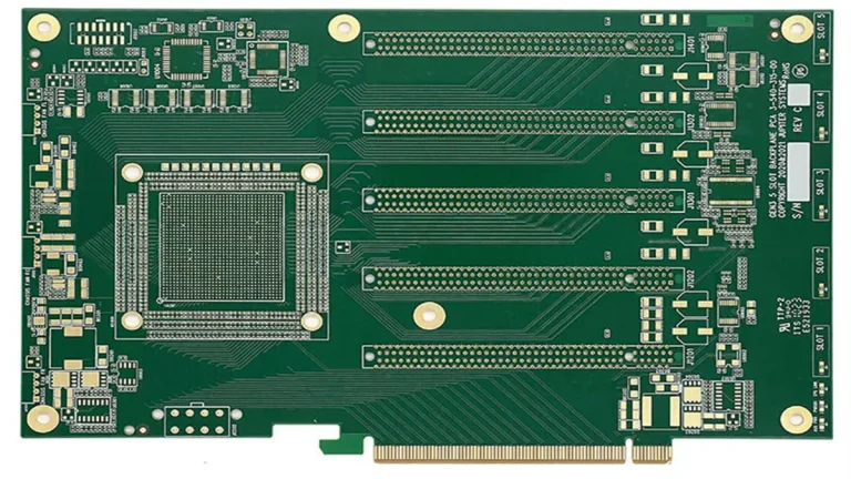
A Gold Finger PCB (also called Gold Finger Printed Circuit Board, Gold Plated PCB Edge, or PCB Edge Connector) is a specialized circuit board featuring electroplated hard gold contacts along one or more edges. These gold-plated edge connectors—commonly referred to as gold fingers, PCB gold contacts, or PCB finger connectors—enable repeated insertion and removal into mating sockets without degradation of electrical conductivity or mechanical integrity.
Unlike standard ENIG (Electroless Nickel Immersion Gold) surface finishes that cover entire pads, hard gold plating on PCB edge connectors is specifically engineered for high-wear applications requiring thousands of insertion cycles. The distinction matters: ENIG deposits a thin, soft gold layer (0.05–0.1 μm) optimized for solderability, while hard gold PCB edge contacts deposit 1.27–5.08 μm (50–200 μin) of cobalt- or nickel-hardened gold designed for abrasion resistance.
At Shenzhen Hongda Circuit Technology Co., Ltd., our dedicated hard gold plating line has processed over 8 million gold finger panels since 2010, serving industries from PCIe accelerator cards and DDR memory modules to industrial backplanes and medical imaging equipment. This guide answers the questions procurement teams and design engineers ask most frequently: What exactly is a gold finger PCB? When should you specify hard gold versus ENIG? How much does it cost? And how do you choose a manufacturer that delivers consistent quality?
What Is a Gold Finger PCB? Definition, Structure & Key Characteristics
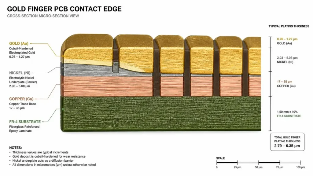
Gold Finger PCB Micro-Section Cross-Section Diagram
A gold finger PCB is a printed circuit board with one or more edges electroplated with hard gold (cobalt-hardened or nickel-hardened) to create durable, low-resistance contact surfaces for edge-card connectors. The gold layer is deposited over electrolytic nickel (typically 3.8–7.6 μm / 150–300 μin) on a copper base, forming a Ni-Au metallurgical system that resists oxidation, corrosion, and mechanical wear across 1,000–10,000+ insertion cycles.
Gold Finger vs. Standard PCB: Structural Differences
| Feature | Standard PCB (ENIG/HASL) | Gold Finger PCB (Hard Gold) |
|---|---|---|
| Gold Type | Immersion gold (soft, 0.05–0.1 μm) | Electroplated hard gold (1.27–5.08 μm) |
| Hardener | None | Cobalt (0.2–0.5%) or Nickel (0.1–0.3%) |
| Base Metal | Electroless nickel (4–6 μm) | Electrolytic nickel (3.8–7.6 μm) |
| Wear Resistance | Low (1–5 insertions) | High (1,000–10,000+ insertions) |
| Contact Resistance | Variable (oxidation-prone) | Stable (<20 mΩ across lifecycle) |
| Primary Function | Solderability | Mechanical/electrical mating |
| Edge Treatment | Standard routing | Chamfer/bevel (20°–45°) |
Why the Name “Gold Finger”?
The term originated from the visual resemblance of parallel gold-plated contact pads to fingers extending from the PCB edge. In technical documentation, you may encounter gold fingers PCB, gold finger board, PCB gold edge contacts, or edge connector PCB—all referring to the same structure. The plural form (gold fingers) typically describes multiple contact pads along one edge, while singular (gold finger) may refer to an individual contact or the general technology.
When Should You Use a Gold Finger PCB?
Specify hard gold PCB edge plating when your application requires:
- Repeated insertion/removal (PCIe cards, RAM modules, hot-swappable drives)
- Low, stable contact resistance (high-speed signal integrity, <20 mΩ)
- Corrosion resistance in harsh environments (industrial controls, marine electronics)
- Long service life without contact degradation (10+ years in telecom infrastructure)
- High-current edge connections (power distribution backplanes, >5A per finger)
→ Read the Complete Gold Finger Basics
Why Are Gold Fingers Used on PCBs? Benefits, Applications & Performance Advantages
Gold fingers are used on PCBs because gold provides the optimal combination of electrical conductivity, corrosion immunity, oxidation resistance, and wear durability among all practical contact materials. Hard gold plating extends these properties across thousands of mechanical insertion cycles while maintaining contact resistance below 20 milliohms—critical for high-speed data transmission in PCIe, DDR, and AI server interconnects.
Why Not ENIG, HASL, or OSP?
This is the most common question from procurement teams comparing surface finish options:
| Finish | Insertion Cycles | Contact Resistance | Cost/Unit | Best Use Case |
|---|---|---|---|---|
| Hard Gold | 1,000–10,000+ | <20 mΩ, stable | High | Edge connectors, wear surfaces |
| ENIG | 1–5 | 50–100 mΩ, degrades | Medium | Solder pads, non-wear contacts |
| HASL (SnPb/SAC) | 0–1 | Unstable, oxidizes | Low | Soldering only, never for mating |
| OSP | 0 | N/A (no contact) | Lowest | Temporary solderability protection |
| Immersion Tin | 5–10 | 30–50 mΩ | Low | Press-fit connectors, limited wear |
Key Insight: ENIG cannot substitute for hard gold in edge connector applications. The immersion gold layer is too thin (0.05–0.1 μm) and too soft (pure gold, ~50 HV) to survive even a single insertion cycle without galling or wear-through. Hard gold, alloyed with cobalt or nickel, achieves 130–200 HV hardness—comparable to hardened steel—and maintains integrity across the product lifecycle.
Performance Advantages of Hard Gold PCB Edge Contacts
- Electrical Conductivity: Gold’s bulk resistivity (2.44 μΩ·cm) is second only to silver among practical contact materials, ensuring minimal signal loss in high-speed designs (PCIe 5.0/6.0, DDR5).
- Oxidation Immunity: Gold does not form oxide layers under normal atmospheric conditions. This eliminates the contact resistance instability that plagues tin, nickel, or copper contacts in humid environments.
- Freting Corrosion Resistance: In vibrating environments (automotive, aerospace), micromotion between mating contacts generates fretting debris that degrades tin or nickel contacts. Gold’s lubricity and chemical stability prevent this failure mode.
- Thermal Stability: Hard gold maintains mechanical properties from -65°C to +200°C, exceeding the operational range of most PCB laminates.
Industry Applications of Gold Finger PCBs
| Industry | Typical Application | Gold Thickness | Insertion Cycles | Critical Requirement |
|---|---|---|---|---|
| AI Server / Data Center | PCIe accelerator cards, NICs, GPU modules | 1.27–2.54 μm (50–100 μin) | 100–500 | Signal integrity at 32 GT/s |
| Networking / Telecom | Router backplanes, switch line cards | 2.54–5.08 μm (100–200 μin) | 1,000–5,000 | 15-year field life |
| Industrial Automation | PLC I/O modules, servo drives | 2.54–5.08 μm (100–200 μin) | 5,000–10,000 | Vibration resistance, hot-swap |
| Medical Devices | MRI gradient controllers, patient monitors | 1.27–2.54 μm (50–100 μin) | 50–200 | Biocompatibility, sterilization |
| Gaming / Consumer | Graphics cards, memory modules | 0.76–1.27 μm (30–50 μin) | 10–50 | Cost optimization |
| Military / Aerospace | Avionics cards, radar processors | 5.08 μm (200 μin) | 10,000+ | MIL-PRF-31032 compliance |
| Automotive | ECU test adapters, diagnostic interfaces | 1.27–2.54 μm (50–100 μin) | 500–2,000 | AEC-Q200, temperature cycling |
→ Explore Industry Applications in Detail
Gold Finger PCB Design Guide: Finger Geometry, Pitch, Chamfer & Layout Rules
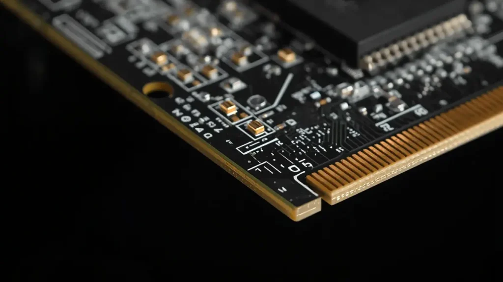
PCIe Gold Finger PCB 30-Degree Bevel Chamfer Detail
Gold finger PCB design requires precise control of finger length (typically 15–30 mm), pitch (1.0–2.54 mm for standard, 0.5–1.0 mm for high-density), chamfer angle (20°–45°), and keepout zones (no copper, mask, or silkscreen within 0.5 mm of the contact edge). The edge must be beveled to prevent stubbing during insertion, and fingers should be plated with hard gold over electrolytic nickel, never ENIG.
Critical Design Parameters
| Parameter | Typical Range | IPC-6012 Requirement | Design Impact |
|---|---|---|---|
| Finger Length | 15–30 mm | Per customer drawing | Determines connector engagement depth |
| Finger Width | 0.8–2.0 mm | ±0.05 mm tolerance | Current-carrying capacity, impedance |
| Pitch (Center-to-Center) | 1.0–2.54 mm (standard) | ±0.05 mm | Connector compatibility |
| High-Density Pitch | 0.5–1.0 mm | ±0.025 mm | PCIe, DDR, M.2 connectors |
| Chamfer Angle | 20°–45° | 30° ±5° (typical) | Insertion force, anti-stubbing |
| Chamfer Length | 1.5–3.0 mm | Per drawing | Guides mating alignment |
| Gold Overhang | 0.0–0.5 mm beyond finger | 0.25 mm max | Prevents peeling, ensures coverage |
| Keepout Zone | 0.5 mm from edge | No copper/mask/silk | Prevents shorting, contamination |
| Nickel Underplate | 3.8–7.6 μm (150–300 μin) | Min 3.8 μm | Diffusion barrier, hardness support |
| Hard Gold Thickness | 0.76–5.08 μm (30–200 μin) | Per IPC-4552 | Wear life, cost balance |
Chamfer Design: The Most Overlooked Parameter
The PCB gold finger chamfer (also called bevel or edge taper) serves three functions:
- Insertion Guidance: The angled lead-in prevents the PCB edge from “stubbing” against the connector housing during mating.
- Contact Wipe: The chamfer creates a progressive engagement that wipes oxide or debris from the mating contact before full electrical engagement.
- Stress Relief: A properly designed chamfer distributes insertion force along the finger length rather than concentrating it at the root.
At Hongda Circuit, our CNC beveling station (Schmoll BZ-3000) achieves ±0.5° angular tolerance and ±0.05 mm length tolerance on chamfers up to 45°. For high-insertion-cycle applications, we recommend a dual-angle chamfer (30° primary + 15° secondary) that optimizes both insertion force and contact wipe.
Keepout and Spacing Rules
- No copper traces within 0.5 mm of the gold finger edge to prevent electrical shorting during insertion.
- No solder mask on gold finger surfaces—mask residue degrades contact resistance.
- No silkscreen legend on or adjacent to fingers—ink particles contaminate mating connectors.
- Minimum finger-to-board-edge spacing: 0.25 mm to prevent gold peeling during routing.
Hard Gold Area Definition
The hard gold area (also called gold plating band or selective gold zone) must be precisely defined in the fabrication drawing. At Hongda Circuit, we use dry film photoresist selective plating to confine hard gold deposition to the finger region only, reducing gold consumption by 60–80% compared to full-edge plating.
→ Download Complete Gold Finger Design Guide
Gold Finger PCB Manufacturing Process: From Copper to Hard Gold
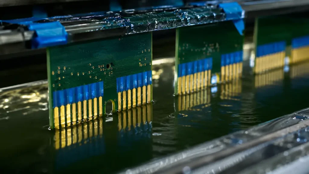
Selective Hard Gold Plating Process for PCB Gold Fingers
Gold finger PCB manufacturing involves 7 critical stages: (1) base copper preparation and etching of finger patterns, (2) electrolytic nickel plating (3.8–7.6 μm) as a diffusion barrier, (3) selective photoresist application to define the hard gold area, (4) electroplated hard gold deposition (0.76–5.08 μm), (5) resist stripping and surface cleaning, (6) CNC chamfering/beveling of the contact edge, and (7) 100% AOI inspection plus contact resistance verification.
Stage-by-Stage Process at Hongda Circuit
Stage 1: Copper Pattern Formation
The gold finger pattern is etched from the outer-layer copper foil (typically 1 oz/35 μm or 2 oz/70 μm for high-current applications). Critical control points:
- Finger width tolerance: ±0.025 mm (±1 mil) for high-density pitch
- Edge straightness: <0.05 mm bow across 300 mm panel length
- Surface roughness: Ra <0.3 μm to ensure uniform nickel deposition
Our MKS laser direct imaging (LDI) system (Orbotech Nuvogo 1000) exposes finger patterns at ±5 μm registration accuracy, eliminating the edge roughness associated with traditional contact printing.
Stage 2: Electrolytic Nickel Plating
Nickel serves as both a diffusion barrier (preventing copper migration into gold) and a mechanical support for the thin gold layer. Our Atotech Nichem MP 2000 nickel bath operates at:
- Thickness: 4.5–6.0 μm (180–240 μin) standard; 7.6 μm (300 μin) for military
- Hardness: 400–500 HV (Vickers) for wear support
- Stress: <200 MPa tensile to prevent finger curling
- Porosity: <5 pores/cm² per ISO 4527
Stage 3: Selective Photoresist Masking
Dry film photoresist (25–50 μm thickness) is laminated over the entire panel, then selectively exposed and developed to expose only the gold finger areas. This selective plating approach is what distinguishes gold finger PCB fabrication from general PCB manufacturing—precise mask alignment prevents gold overflow onto adjacent traces while ensuring complete finger coverage.
Our Orbotech Paragon-X automated exposure system achieves ±8 μm layer-to-layer registration, critical for 0.5 mm pitch fingers where mask misalignment would expose adjacent solder mask or cover part of the finger.
Stage 4: Hard Gold Electroplating
The heart of gold finger manufacturing. Our Umicore Auruna 3110 hard gold electrolyte deposits cobalt-hardened gold with:
- Gold content: 8 g/L (optimized for throwing power)
- Cobalt hardener: 0.3–0.5 wt% (achieves 150–180 HV)
- pH: 4.0–4.5 (citrate buffer)
- Temperature: 45–55°C
- Current density: 1.5–3.0 A/dm²
- Deposition rate: 0.15 μm/minute
Thickness Control: Real-time XRF (X-ray fluorescence) monitoring every 15 minutes ensures thickness uniformity ±10% across the panel. For a 2.54 μm (100 μin) specification, our process maintains 2.29–2.79 μm (90–110 μin) on every finger.
Stage 5: Resist Stripping & Surface Cleaning
After gold plating, the photoresist is stripped in alkaline solution (NaOH, 3–5%, 50°C), followed by:
- Micro-etch: 0.5–1.0 μm copper removal to eliminate gold contamination on non-finger areas
- Acid cleaning: H₂SO₄/H₂O₂ to remove organic residues
- DI water rinse: Resistivity >10 MΩ·cm
- Hot air drying: 80°C to prevent water staining
Stage 6: CNC Chamfering / Beveling
The contact edge is machined to the specified chamfer angle using a diamond-coated V-bit router (Schmoll BZ-3000):
- Spindle speed: 30,000 RPM
- Feed rate: 2,000 mm/minute
- Depth control: ±0.025 mm
- Surface finish: Ra <0.4 μm (critical for low-contact-resistance mating)
For dual-angle chamfers, we perform two passes with different V-bits, achieving angular transitions within ±0.5°.
Stage 7: Final Inspection & Electrical Verification
| Inspection Method | Equipment | Criteria | Coverage |
|---|---|---|---|
| AOI | Orbotech Discovery 8800 | No scratches, contamination, mask residue | 100% of fingers |
| XRF Thickness | Fischer XDV-SDD | Gold ±10%, Nickel ±15% | 100% fingers, 5 points/finger |
| Contact Resistance | Custom 4-wire probe | <20 mΩ per finger | 100% sampling |
| Chamfer Verification | Keyence IM-8000 | Angle ±1°, length ±0.05 mm | 100% of edges |
| Adhesion Tape Test | 3M 600 tape | No gold peel after tape pull | AQL 1.0 per lot |
| Visual Inspection | 10× stereo microscope | No pits, discoloration, plating nodules | 100% |
→ View Detailed Manufacturing Process
Gold Finger PCB Specifications: Thickness, Tolerance, Hardness & Performance Metrics
Gold finger PCB specifications are governed by IPC-4552 (electroplated gold for edge connectors) and IPC-6012 (performance specification). Key metrics include: hard gold thickness 0.76–5.08 μm (30–200 μin), nickel underplate 3.8–7.6 μm (150–300 μin), gold hardness 130–200 HV (Knoop), contact resistance <20 mΩ, and insertion force 0.5–2.0 N per finger depending on pitch and chamfer design.
Complete Specification Table
| Specification | IPC-4552 Requirement | Hongda Circuit Standard | Military/Aerospace |
|---|---|---|---|
| Hard Gold Thickness | 0.76–5.08 μm (30–200 μin) | 1.27–2.54 μm (50–100 μin) | ≥5.08 μm (200 μin) |
| Gold Hardness (Knoop) | 130–200 HK | 150–180 HK | 160–200 HK |
| Gold Purity | 99.0% min | 99.5% (cobalt-hardened) | 99.7% |
| Nickel Thickness | 3.8–7.6 μm (150–300 μin) | 4.5–6.0 μm (180–240 μin) | ≥7.6 μm (300 μin) |
| Nickel Hardness | 400–500 HV | 450–500 HV | ≥500 HV |
| Contact Resistance | <50 mΩ | <20 mΩ | <15 mΩ |
| Insertion Force (per finger) | Per connector spec | 0.5–1.5 N | 0.8–2.0 N |
| Wear Life (min cycles) | Per application | 1,000–5,000 | 10,000+ |
| Chamfer Angle | 20°–45° | 30° ±2° | 30° ±1° |
| Finger Width Tolerance | ±0.05 mm | ±0.025 mm | ±0.015 mm |
| Pitch Tolerance | ±0.05 mm | ±0.025 mm | ±0.015 mm |
| Edge Straightness | <0.1 mm/300 mm | <0.05 mm/300 mm | <0.03 mm/300 mm |
| Surface Roughness (Ra) | <0.8 μm | <0.4 μm | <0.3 μm |
Gold Thickness Selection Guide by Application
| Gold Thickness | μin | μm | Typical Application | Cost Impact |
|---|---|---|---|---|
| Flash Gold | 3–10 | 0.08–0.25 | Prototyping, very low cycle | Baseline |
| Standard | 30–50 | 0.76–1.27 | Consumer electronics, gaming | +15% |
| Enhanced | 50–100 | 1.27–2.54 | Networking, AI servers, medical | +35% |
| Heavy | 100–200 | 2.54–5.08 | Industrial, automotive, telecom | +60% |
| Military | 200+ | 5.08+ | Aerospace, military, extreme wear | +100% |
Cost Note: Gold is priced by gram, and PCB gold consumption is calculated by surface area × thickness × density (19.32 g/cm³). A 300 mm × 200 mm panel with 30 mm × 2 mm fingers (10 fingers) at 2.54 μm gold consumes approximately 0.37 grams of gold. At $65/gram (2026 market), the gold material cost alone is ~$24 per panel—explaining why thickness optimization is critical for cost-sensitive applications.
→ Read Full Specification Guide
Gold Finger PCB Standards: IPC, RoHS, REACH & Industry Compliance
Gold finger PCBs must comply with IPC-4552 (electroplated gold for printed board edge contacts), IPC-6012 (performance and qualification), IPC-A-600 (acceptability), and environmental directives RoHS (2011/65/EU) and REACH (EC 1907/2006). For military applications, MIL-PRF-31032 and MIL-STD-202 apply. Automotive requires IATF 16949 and often AEC-Q200 validation.
IPC Standard Hierarchy for Gold Finger PCBs
| Standard | Scope | Gold Finger Relevance | Key Requirements |
|---|---|---|---|
| IPC-4552 | Electroplated gold for edge connectors | Primary standard | Gold thickness, hardness, nickel underplate, adhesion, porosity testing |
| IPC-6012 | Rigid PCB qualification | Performance class definition | Class 2 (industrial), Class 3 (high-performance), Class 3/A (space) |
| IPC-A-600 | PCB acceptability | Visual inspection criteria | Plating nodules, discoloration, edge roughness, chamfer defects |
| IPC-A-610 | Assembly acceptability | Post-assembly gold finger integrity | No solder contamination on gold, no mechanical damage |
| IPC-TM-650 | Test methods | Laboratory validation | 2.4.18 (adhesion), 2.4.24 (porosity), 2.4.42 (thickness) |
| IPC-2221/2222 | Generic/design standards | Edge connector design rules | Keepout zones, chamfer geometry, current density |
| IPC-1752A | Material declaration | RoHS/REACH compliance | Gold source, cobalt/nickel hardener content, conflict minerals |
Environmental Compliance
| Directive | Requirement | Gold Finger Impact | Hongda Circuit Compliance |
|---|---|---|---|
| RoHS 3 (2011/65/EU) | Restricts Cd, Pb, Hg, Cr(VI), PBB, PBDE, 4 phthalates | Gold itself is RoHS-compliant; cobalt hardener must be <0.1% restricted substances | Full material declarations per IPC-1752A |
| REACH (EC 1907/2006) | SVHC (Substances of Very High Concern) disclosure | Cobalt salts in plating baths may trigger SVHC if >0.1% w/w in article | Closed-loop bath recycling; <0.05% residual cobalt |
| Conflict Minerals (Dodd-Frank) | Disclosure of 3TG (tin, tantalum, tungsten, gold) sourcing | Gold must be from certified conflict-free sources | RMI-certified gold supplier (Umicore) |
| UL 94V-0 | Flammability rating | Laminate flammability, not gold-specific | All laminates UL 94V-0 certified |
| WEEE (2012/19/EU) | End-of-life recycling | Gold recovery from scrap PCBs | Partnership with certified e-waste recycler |
Industry-Specific Standards
| Industry | Standard | Gold Finger Requirement |
|---|---|---|
| Automotive | IATF 16949, AEC-Q200 | PPAP Level 3, thermal cycling -40°C to +150°C |
| Medical | ISO 13485, IEC 60601 | Biocompatibility ISO 10993, sterilization compatibility |
| Aerospace | MIL-PRF-31032, MIL-STD-202 | 5.08 μm gold min, 10,000 insertion cycles, outgassing testing |
| Telecom | Telcordia GR-78 | 20-year field life, humidity bias 85°C/85%RH |
| AI Server | OCP (Open Compute Project) | PCIe signal integrity, gold thickness consistency for impedance |
→ Explore IPC Standards in Detail
Gold Finger PCB Applications: Industry-by-Industry Use Cases
Gold finger PCBs are used across eight primary industries: AI servers (PCIe cards, GPU modules), networking/telecom (backplanes, line cards), industrial automation (PLC I/O, servo drives), medical devices (imaging controllers, patient monitors), gaming/consumer (graphics cards, RAM modules), military/aerospace (avionics, radar), automotive (ECU test adapters), and test/measurement (ATE interfaces, oscilloscope modules).
AI Server & Data Center: The Fastest Growing Segment
AI server motherboards and accelerator cards represent the highest-volume growth market for gold finger PCBs in 2026. Key requirements:
- PCIe 5.0/6.0 compatibility: 32–64 GT/s signaling demands contact resistance <15 mΩ and impedance control ±5%
- High-current fingers: GPU modules draw 300–600W through edge connectors; finger current density reaches 5–10 A/mm²
- Thermal cycling: Power management induces -40°C to +125°C swings; gold fingers must survive 1,000+ cycles
- 0.5 mm pitch: M.2 and U.2 connectors require ±0.025 mm pitch tolerance
Hongda Circuit Case Study: We supply PCIe 5.0 accelerator cards for a leading AI chip vendor, achieving <18 mΩ contact resistance and 0 insertion failures across 500-cycle qualification.
Networking & Telecommunications: Long-Life Infrastructure
Router and switch backplanes use gold finger PCBs for line card insertion:
- Backplane density: 100+ fingers per edge, 2.54 mm pitch, 20+ year service life
- Environmental stress: Central office temperatures 0°C to +55°C with 95% RH; gold prevents humidity-induced contact degradation
- Hot-swap requirement: Live insertion demands low insertion force (<1 N/finger) and anti-arcing chamfer design
Industrial Automation: Extreme Durability
PLC I/O modules and servo drive interfaces require the highest mechanical durability:
- Insertion cycles: 5,000–10,000+ for maintenance-replaceable modules
- Vibration resistance: IEC 60068-2-6 (sinusoidal 5–500 Hz, 2g) without contact fretting
- Chemical exposure: Oil mist, coolant spray, and cleaning solvents; gold’s chemical inertness is essential
Medical Devices: Biocompatibility & Precision
MRI gradient controllers and patient monitoring modules:
- Biocompatibility: ISO 10993-5 cytotoxicity testing for patient-contacting equipment
- Sterilization compatibility: Autoclave (134°C steam), gamma radiation, and EtO sterilization without gold degradation
- Low-noise contacts: <10 mΩ contact resistance for sensitive analog signal paths
Gaming & Consumer Electronics: Cost-Optimized Performance
Graphics cards and DDR memory modules balance performance with cost:
- Standard thickness: 0.76–1.27 μm (30–50 μin) gold—sufficient for 50–100 insertions during assembly and upgrade
- Panel optimization: Multiple cards per panel (4-up, 6-up) to amortize gold plating setup costs
- Lead time: 5–7 days for standard gaming card production
→ View All Industry Applications
Gold Finger PCB Cost Guide: Pricing Factors, Optimization Strategies & Budget Planning
Gold finger PCB cost is driven by five primary factors: gold thickness (0.76–5.08 μm, accounting for 30–60% of total cost), finger length and count (more fingers = more gold area), panel size and utilization (larger panels reduce per-unit overhead), order quantity (MOQ 100+ panels for cost efficiency), and IPC class (Class 3 adds 20–40% inspection and documentation cost). Typical pricing ranges from $15/m² for flash gold prototypes to $200+/m² for heavy gold, Class 3, military-grade boards.
Cost Breakdown by Component
| Cost Component | % of Total (Standard 1.27 μm) | % of Total (Heavy 5.08 μm) | Cost Driver |
|---|---|---|---|
| Gold Material | 35% | 55% | Thickness × area × $65/g market price |
| Nickel Plating | 8% | 5% | Bath chemistry, electricity, labor |
| Photoresist & Masking | 10% | 8% | Dry film cost, exposure time |
| Chamfering / Beveling | 5% | 4% | CNC machine time, diamond bit wear |
| Inspection (XRF, AOI) | 12% | 10% | Equipment depreciation, labor |
| Base PCB Fabrication | 20% | 14% | Layer count, laminate, etching |
| Overhead & Margin | 10% | 8% | Facility, engineering, profit |
Gold Thickness vs. Cost Relationship
| Thickness (μm) | Thickness (μin) | Relative Cost | Typical MOQ | Best For |
|---|---|---|---|---|
| 0.76 | 30 | 1.0× (baseline) | 50 panels | Prototypes, consumer |
| 1.27 | 50 | 1.4× | 100 panels | Standard industrial |
| 2.54 | 100 | 2.1× | 100 panels | Networking, AI servers |
| 5.08 | 200 | 3.8× | 250 panels | Military, aerospace |
| 7.62 | 300 | 5.5× | 500 panels | Extreme wear, custom |
Cost Optimization Strategies for Procurement
- Panelization Efficiency: Design for standard panel sizes (457 mm × 610 mm or 18” × 24”) to maximize gold finger count per panel. A 6-up panel reduces per-unit gold plating overhead by 40% compared to single-up.
- Thickness Rationalization: Specify the minimum gold thickness that meets the application’s insertion cycle requirement. Don’t default to 2.54 μm for a 50-cycle gaming card when 1.27 μm suffices.
- Selective Plating: Ensure your manufacturer uses true selective plating (photoresist masking) rather than full-edge plating. This reduces gold consumption by 60–80% on panels with non-contact edges.
- Batch Consolidation: Combine multiple SKU orders into a single production run. Gold plating bath setup (cleaning, chemistry adjustment, dummy plating) costs $300–500 per batch regardless of panel count.
- Nickel Thickness Optimization: IPC-4552 permits 3.8–7.6 μm nickel. For non-military applications, 4.5–5.0 μm provides adequate diffusion barrier performance at lower cost than 7.6 μm.
- Lead Time Flexibility: Standard 10–12 day lead time is 30% less expensive than 5-day expedite. Plan procurement cycles to avoid premium charges.
Requesting a Gold Finger PCB Quote: What Information to Provide
To receive an accurate gold finger PCB quote within 24 hours, provide:
- Gerber files with separate gold finger layer or clear edge connector annotation
- Gold thickness specification (μm or μin) and hardness requirement (if non-standard)
- Finger dimensions: Length, width, pitch, and total count per board
- Chamfer angle and length (or “standard 30°” if unspecified)
- Order quantity: Annual volume, first article quantity, production ramp plan
- IPC class: Class 2 (standard) or Class 3 (high-reliability)
- Industry/application: Determines testing and documentation requirements
- Delivery schedule: Standard or expedited; blanket order with releases preferred
→ Get a Custom Gold Finger PCB Quote
Gold Finger PCB vs ENIG PCB: When to Choose Hard Gold vs Immersion Gold
Choose hard gold (electroplated) for edge connectors requiring mechanical wear resistance (>100 insertion cycles), stable contact resistance, and long field life. Choose ENIG (immersion gold) for solder pads where solderability is the primary requirement and no mechanical mating occurs. Hard gold costs 3–5× more than ENIG per unit area but is irreplaceable in edge connector applications. Never use ENIG for gold fingers—it will fail within 1–10 insertion cycles.
Side-by-Side Comparison
| Attribute | Hard Gold PCB Edge | ENIG PCB Surface |
|---|---|---|
| Deposition Method | Electroplating (DC or pulse) | Chemical displacement (autocatalytic) |
| Gold Thickness | 0.76–5.08 μm (30–200 μin) | 0.05–0.1 μm (2–4 μin) |
| Gold Purity | 99.0–99.7% (cobalt/nickel hardened) | 99.9% (pure, soft) |
| Hardness (Knoop) | 130–200 HK | 50–70 HK |
| Wear Resistance | 1,000–10,000+ cycles | 1–5 cycles |
| Contact Resistance | <20 mΩ, stable | 50–100 mΩ, increases with oxidation |
| Corrosion Resistance | Excellent (no oxide formation) | Good (nickel barrier protects) |
| Solderability | Poor (gold embrittlement risk) | Excellent |
| Wire Bondability | Possible (thick gold) | Excellent (thin, pure gold) |
| Cost per m² | $50–200+ | $8–15 |
| Best Application | Edge connectors, wear surfaces | Solder pads, wire bond pads |
The “Black Pad” Risk in ENIG
A critical failure mode unique to ENIG is “black pad”—hyperactive corrosion of the electroless nickel underlayer that creates a brittle, dark interface. Under mechanical stress (even minor), the gold layer separates from the nickel, causing catastrophic joint failure. While black pad primarily affects solder joints, it demonstrates why ENIG’s nickel structure is unsuitable for mechanical wear applications. Hard gold uses electrolytic nickel (columnar, dense grain structure) rather than electroless nickel (nodular, porous), eliminating black pad risk entirely.
Can You Use Both on the Same PCB?
Yes—and this is common in complex designs. At Hongda Circuit, we manufacture boards with:
- Hard gold on edge connector fingers (wear resistance)
- ENIG on BGA and SMT pads (solderability)
- OSP on through-hole component pads (cost reduction)
- Immersion silver on RF pads (skin effect optimization)
This selective surface finish approach requires precise photoresist masking but optimizes both performance and cost.
→ Read Full ENIG vs Hard Gold Comparison
How to Choose a Gold Finger PCB Manufacturer: Procurement Checklist & Supplier Evaluation
Evaluate gold finger PCB manufacturers on 7 critical capabilities: (1) dedicated hard gold plating line with real-time thickness monitoring, (2) selective plating photoresist process (not full-edge plating), (3) CNC chamfering equipment with ±1° angular tolerance, (4) XRF thickness verification on every finger, (5) IPC-4552 and IPC-6012 Class 3 certification, (6) in-house microsection and contact resistance testing, and (7) demonstrated experience in your target industry (AI server, automotive, medical, etc.).
Supplier Capability Scoring Matrix
| Capability | Weight | Basic (1–3) | Advanced (4–7) | World-Class (8–10) |
|---|---|---|---|---|
| Hard Gold Plating Line | 20% | Outsourced or shared line | Dedicated line, manual XRF | Dedicated line, automated XRF, bath chemistry AI control |
| Selective Plating | 15% | Full-edge plating only | Manual photoresist masking | Automated LDI masking, ±8 μm registration |
| Chamfering Equipment | 15% | Manual sanding | CNC V-bit, ±2° tolerance | CNC diamond V-bit, ±0.5°, dual-angle capability |
| Thickness Verification | 15% | Spot check, caliper | XRF, 10% sampling | XRF, 100% fingers, 5 points each, SPC charting |
| IPC Certification | 10% | IPC-A-600 | IPC-6012 Class 2 | IPC-6012 Class 3, MIL-PRF-31032, IATF 16949 |
| In-House Testing | 10% | Visual only | AOI, basic microsection | AOI, SEM/EDX, contact resistance, insertion force |
| Industry Experience | 10% | Consumer only | Mixed industries | AI server, automotive, medical, military references |
| Lead Time | 5% | 15+ days | 10–12 days | 7–10 days standard, 5-day expedite |
Red Flags: When to Disqualify a Supplier
- No dedicated gold plating line: Shared lines with other surface finishes (HASL, ENIG) risk cross-contamination and inconsistent gold quality.
- Cannot provide XRF thickness data: XRF (X-ray fluorescence) is the only non-destructive method to verify gold and nickel thickness. A supplier without XRF cannot control their process.
- Full-edge plating only: This increases your gold cost by 60–80% and may deposit gold on areas where solder mask adhesion is required.
- No chamfering capability: Chamfering is not optional for edge connectors. Manual sanding produces inconsistent angles and rough surfaces that damage mating connectors.
- Outsources microsection testing: In-house microsection capability indicates serious quality investment. Outsourcing adds 3–5 days to failure analysis and suggests limited technical depth.
The Hongda Circuit Difference
| Evaluation Criterion | Hongda Circuit Capability |
|---|---|
| Gold Plating Line | 2 dedicated hard gold lines (Umicore Auruna chemistry), 500 panels/day capacity |
| Selective Plating | Orbotech Paragon-X LDI masking, ±8 μm layer-to-layer registration |
| Chamfering | Schmoll BZ-3000 CNC, diamond V-bits, dual-angle capability, ±0.5° tolerance |
| Thickness Control | Fischer XDV-SDD XRF, 100% finger coverage, real-time SPC charting |
| Certifications | IPC-6012 Class 3, IATF 16949, ISO 13485, MIL-PRF-31032 (pending) |
| Testing | In-house SEM/EDX, contact resistance 4-wire probe, insertion force gauge |
| Experience | 8M+ gold finger panels since 2010; AI server, automotive, medical references |
| Lead Time | 7–10 days standard; 5-day expedite available |
Frequently Asked Questions (FAQ): Gold Finger PCB
What is a PCB Gold Finger?
A PCB gold finger is an electroplated hard gold contact pad along the edge of a printed circuit board, designed for repeated insertion into a mating connector socket. It consists of a copper base, electrolytic nickel diffusion barrier (3.8–7.6 μm), and cobalt-hardened gold wear layer (0.76–5.08 μm). Gold fingers enable reliable electrical and mechanical connection in PCIe cards, memory modules, industrial I/O, and backplane interfaces.
How Thick Should PCB Gold Plating Be?
PCB gold finger thickness ranges from 0.76 μm (30 μin) for cost-sensitive consumer applications to 5.08 μm (200 μin) for military/aerospace. The optimal thickness depends on insertion cycle requirements:
50–100 cycles: 0.76–1.27 μm (gaming, consumer)
500–2,000 cycles: 1.27–2.54 μm (networking, AI servers, automotive)
5,000–10,000+ cycles: 2.54–5.08 μm (industrial, telecom, military)
IPC-4552 specifies minimum 0.76 μm; Hongda Circuit recommends 1.27 μm as the standard for general industrial applications.
What Is the Difference Between Hard Gold and ENIG on PCBs?
Hard gold is electroplated, 0.76–5.08 μm thick, cobalt/nickel-hardened (130–200 HK), designed for mechanical wear resistance (1,000+ cycles). ENIG is immersion-deposited, 0.05–0.1 μm thick, pure soft gold (50–70 HK), designed for solderability only (1–5 cycles). Hard gold costs 3–5× more per area but is mandatory for edge connectors; ENIG will fail catastrophically if used for mating surfaces.
Why Do PCB Gold Fingers Wear Out?
Gold fingers wear through abrasive wear (mechanical rubbing against mating contacts), adhesive wear (micro-welding at high current), and fretting corrosion (vibration-induced micromotion generating oxide debris). Wear rate increases with insertion force, contact contamination, and inadequate chamfer design. Proper hard gold thickness, cobalt hardening, and chamfer optimization can extend wear life from 100 cycles to 10,000+ cycles.
Can Worn Gold Fingers Be Repaired?
Repair is generally not recommended. Re-plating worn gold fingers requires stripping the old gold, re-activating the nickel, and re-plating—processes that risk damaging the underlying copper or delaminating the board edge. For high-value boards (military, medical), some specialized shops offer selective brush plating as a temporary fix, but the repaired area will not match original hardness or thickness uniformity. Prevention through proper specification is far more cost-effective than repair.
What Is the Minimum Pitch for Gold Finger PCBs?
Standard gold finger pitch is 1.0–2.54 mm for industrial and networking connectors. High-density applications achieve 0.5–1.0 mm pitch (M.2, U.2, custom PCIe variants). At 0.5 mm pitch, manufacturing challenges include:
Photoresist masking resolution (minimum 25 μm line/space)
Nickel plating uniformity between closely spaced fingers
Chamfering without damaging adjacent fingers
XRF thickness measurement resolution (requires <50 μm spot size)
Hongda Circuit manufactures 0.5 mm pitch gold fingers with ±0.025 mm tolerance using LDI masking and micro-focus XRF.
Making the Right Gold Finger PCB Decision
Gold finger PCB technology sits at the intersection of electrical engineering, materials science, and precision manufacturing. The decision to specify hard gold over ENIG, to choose 1.27 μm versus 2.54 μm thickness, or to design a 30° versus 45° chamfer has measurable consequences for product reliability, field life, and total cost of ownership.
For procurement professionals, the key takeaway is this: not all gold plating is equal. A supplier with a shared ENIG line and manual chamfering cannot deliver the consistency required for AI server PCIe cards or automotive ECU interfaces. The equipment matters—dedicated hard gold lines, automated XRF monitoring, CNC chamfering, and in-house microsection capability separate world-class manufacturers from commodity fabricators.
At Shenzhen Hongda Circuit Technology Co., Ltd., our $12 million investment in dedicated hard gold manufacturing infrastructure reflects our commitment to this specialization. From 50 μm micro-focus XRF verification to AI-driven SPC process control, every step of our gold finger production is engineered for the insertion-cycle demands of modern electronics.
Ready to specify your next gold finger PCB? Request a quote with your Gerber files and application requirements, and our engineering team will recommend the optimal gold thickness, chamfer design, and testing protocol for your project.
Shenzhen Hongda Circuit Technology Co., Ltd. Hard Gold PCB Manufacturing | Gold Finger Specialists | IPC-4552 Certified www.pcbkr.com | sales@pcbkr.com
About Author
David Chen https://www.linkedin.com/in/pcbcoming
David Chen boasts an extensive professional background in PCBA manufacturing, PCBA testing, and PCBA optimization, with specialized expertise in high-precision PCBA fault analysis and rigorous PCBA reliability testing. The author has worked with high-layer-count server PCB fabrication, ultra-low-loss backplane stackups, and thermo-mechanical reliability optimization for AI infrastructure projects involving 112G and 224G PAM4 architectures. Skilled in complex circuit design and cutting-edge advanced PCB manufacturing processes, he delivers solutions that elevate product durability and performance across industrial applications. His technical articles focusing on PCBA manufacturing workflows and testing methodologies are widely cited by industry peers, research institutions, and technical platforms, solidifying his reputation as a recognized technical authority in the global circuit board manufacturing sector.