High-Tg FR4 Multilayer PCB Stackup Design: The Complete Procurement Guide for OEM Buyers
What Is a High-Tg PCB Stackup?
A High-Tg PCB stackup utilizes base laminate materials with a glass transition temperature (Tg) of ≥ 170°C — compared to standard FR4 at 130–140°C. It provides superior mechanical rigidity, reduced Z-axis thermal expansion, and enhanced delamination resistance during lead-free soldering and harsh thermal cycling.
For procurement teams, this translates to one thing: boards that survive where standard FR4 fails. If your product operates above 100°C, undergoes multiple reflow cycles, or demands IPC Class 3 reliability, High-Tg is not optional. It is a material prerequisite that directly impacts warranty costs, field failure rates, and supplier audit scores.
At Shenzhen Hongda Circuit Technology Co., Ltd. (PCBKR), we fabricate High-Tg multilayer boards up to 120 layers for AI server backplanes and process them through mSAP (Modified Semi-Additive Process) lines capable of sub-20μm trace geometry. The stackup decisions made at the quoting stage determine whether those boards pass thermal cycling or delaminate in the field.
Why High-Tg Stackup Design Matters in Modern Electronics Procurement
The shift toward AI infrastructure, 800V EV powertrains, and 6G telecommunications has rewritten procurement criteria. Buyers are no longer just comparing price-per-square-inch. They are vetting signal integrity margins, thermal management architectures, and material traceability.
Consider the numbers. A standard server PCB might carry 12–16 layers. An AI server backplane for Rubin or Blackwell architecture demands 60–120 layers with 224Gbps PAM4 signaling. The Z-axis CTE mismatch between standard FR4 and copper barrels becomes catastrophic at those layer counts. High-Tg substrates — paired with low-loss dielectrics like Panasonic Megtron 8 or Isola 370HR — shrink that mismatch and keep via barrels intact through thousands of thermal cycles.
Procurement managers who understand stackup design speak the same language as their engineering teams. They ask better questions during factory audits. They catch DFM risks before PO release. And they avoid the hidden cost of late-stage redesigns.
Core Design Principles for High-Tg Multilayer PCB Stackups
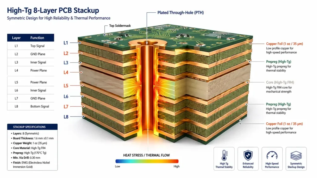
High-Tg 8-Layer PCB Stackup Structure & Thermal Flow Diagram – Hongda Circuit
Symmetry in Construction: Eliminate Warp Before It Starts
Unbalanced copper distribution is the leading cause of board warp during reflow. In High-Tg multilayer designs — where resin modulus is higher and material recovery is lower — asymmetry amplifies every thermal stress.
The rule: Mirror copper weights and dielectric thicknesses around the center core. If Layer 2 carries 1oz copper, Layer N-1 carries 1oz. If the prepreg between L1-L2 is 2116, match it on the bottom side. At PCBKR, our DFM engineers run copper balance simulations on every stackup before panelization. We have seen too many 12-layer boards bow beyond 0.75% simply because a buyer accepted an asymmetric stackup to save $0.40 per panel.
Z-Axis CTE Management: Protect the Via Barrel
Standard FR-4 expands roughly 250–350 ppm/°C above Tg in the Z-axis. High-Tg materials like ITEQ IT-180A or Shengyi S1000-2 cut that to 180–220 ppm/°C. That difference determines whether your plated through-holes crack after 500 thermal cycles or survive 2,000.
For procurement, this means verifying two things in the supplier’s material certificate:
- Tg by DSC (Differential Scanning Calorimetry) per IPC-TM-650 2.4.25 — not just the datasheet claim.
- Z-axis CTE above Tg per IPC-TM-650 2.4.24, typically ≤ 3.0% for High-Tg grades.
Impedance & Dielectric Stability Across Temperature
High-Tg prepregs offer more consistent Dk values across operating temperatures, but consistency depends on resin content and glass style. A 2116 prepreg from one lot can vary ±0.2 in Dk if the supplier does not control resin flow.
For controlled impedance stackups — especially 100Ω differential pairs in 224Gbps designs — that variance shifts impedance by ±5-7Ω. At PCBKR, we validate every prepreg lot with TDR test coupons and adjust trace widths in the CAM stage to hold ±5% impedance tolerance on production panels.
Reflow Thermal Margin: Td and Lead-Free Compatibility
High-Tg does not automatically mean High-Td. The decomposition temperature (Td, measured by TGA at 5% weight loss) must exceed 340°C to withstand multiple lead-free reflow cycles at 260°C peak. Materials like Isola 370HR hit Td ≈ 360°C. Some budget High-Tg laminates barely clear 320°C — fine for one reflow, risky for double-sided assembly or rework.
When auditing suppliers, request the IPC-4101 slash sheet compliance for the specific laminate they plan to use. Do not accept “High-Tg FR4” as a generic description.
How to Evaluate a High-Tg PCB Manufacturer’s Technical Capabilities

Advanced LDI Laser Direct Imaging Machine in Cleanroom
Advanced Fabrication Equipment & Process Nodes
The gap between a PCB shop that “can do High-Tg” and one that masters it is measured in capital equipment. Here is what procurement teams should look for during virtual or on-site factory audits:
| Capability | Why It Matters for High-Tg | PCBKR Specification |
| LDI (Laser Direct Imaging) | Eliminates photo-tool registration errors; critical for fine-line High-Tg boards where etch tolerance is tight | ±25μm layer alignment accuracy |
| mSAP Process | Enables sub-20μm line/space on High-Tg substrates for IC substrates and mobile HDI | 30/30μm production; sub-20μm prototype |
| Laser Drilling | Creates microvias (≤75μm) in dense High-Tg builds without mechanical drill wander | 75μm microvia diameter; any-layer interconnect |
| Sequential Lamination | Builds complex 6+N+6 or 4+N+4 HDI structures with controlled stress relief between cycles | Up to 6+N+6 mass production; 120-layer samples |
| AI-Driven AOI/AVI | Detects delamination precursors and plating voids that traditional AOI misses | Deep learning-based defect classification |
| Digital Twin MES | Provides real-time traceability of material batches, press cycles, and impedance data | Full lot traceability from copper foil to shipping |
A supplier running traditional contact exposure and mechanical drilling can fabricate 4-layer High-Tg boards. They cannot reliably produce 12-layer controlled-impedance HDI with 0.3mm BGA pitch. Match the equipment list to your product roadmap, not just your current revision.
Material Ecosystem & Supply Chain Resilience
High-Tg laminates are not commodities. Lead times for Panasonic Megtron 8 or Rogers RO4350B can stretch 8–12 weeks during capacity crunches. A qualified supplier should stock multiple approved laminates for the same application and provide cross-reference guidance.
At PCBKR, we maintain strategic inventory of: – Shengyi S1000-2 (Tg 170°C, cost-optimized industrial grade) – Isola 370HR (Tg 180°C, low CTE, preferred for automotive) – ITEQ IT-180A (Tg 180°C, high thermal reliability, medical/aerospace) – Panasonic Megtron 7/8 (Low Df ≤ 0.0015, 224Gbps AI server grade)
If your primary supplier relies on a single laminate source, you are one allocation notice away from a line-down situation.
Quality Certifications & Compliance Matrix
High-Tg boards for mission-critical applications demand more than ISO 9001. Procurement teams should verify the specific scope of each certification. A supplier with ISO 13485 on file but no medical device PCB scope is not qualified for your diagnostic imaging project.
PCBKR Certification Portfolio: – ISO 9001:2015 (Quality Management) – ISO 14001:2015 (Environmental Management) – IATF 16949:2016 (Automotive — EV powertrain, ADAS, BMS) – ISO 13485:2016 (Medical Device — imaging, patient monitoring) – IPC-6012 Class 3/3A (High-Reliability Performance) – AS9100D (Aerospace & Defense) – RoHS 3.0 / REACH / UL Recognition
Request the certificate scope pages, not just the cover. Verify the certification body is accredited (e.g., UKAS, ANAB).
DFM Engineering Support & NPI Velocity
The best High-Tg stackup in the world fails if the fabricator cannot manufacture it. Early DFM engagement — before Gerber freeze — catches stackup asymmetries, aspect ratio violations, and impedance discontinuities.
PCBKR operates a 30-minute inquiry response and 1-hour engineering evaluation protocol. Our DFM team reviews stackup proposals against our press capacity, material stock, and impedance modeling tools before the RFQ is even finalized. For buyers, this eliminates the 3-day delay that typically follows a “we need to check with engineering” email.
Recommended High-Tg Stackup Examples for Procurement Planning
Engineers click through to supplier websites for actionable stackup data, not generic definitions. Below are verified configurations from our 2026 production floor, with material callouts and impedance targets.
4-Layer High-Tg Stackup for Industrial Controls
| Layer | Function | Material | Copper Weight | Thickness |
| L1 (Top) | Signal + Components | Shengyi S1000-2 | 1oz (35μm) | 0.2mm prepreg |
| L2 | Ground Plane | Core FR4-High Tg | 1oz | 1.0mm core |
| L3 | Power Plane | Core FR4-High Tg | 1oz | 1.0mm core |
| L4 (Bottom) | Signal + Components | Shengyi S1000-2 | 1oz | 0.2mm prepreg |
Total Thickness: 1.6mm ± 0.16mm
Impedance Target: 50Ω single-ended (L1/L4 referencing L2/L3)
Application: PLC controllers, motor drives, power inverters
Why It Works: Symmetrical prepreg thicknesses (2116 style) balance thermal stress. The 1.0mm core provides rigidity for heavy components. S1000-2 keeps cost down while delivering Tg 170°C and Td > 340°C.
8-Layer 1.6mm Controlled Impedance Stackup for 224Gbps Networking
| Layer | Function | Material | Copper | Notes |
| L1 | Signal | Panasonic Megtron 8 | 0.5oz | 100Ω diff, 224Gbps |
| L2 | Ground | Megtron 8 core | 1oz | Solid reference |
| L3 | Signal | Prepreg 1080 | 0.5oz | 50Ω SE |
| L4 | Power | Core | 1oz | Split planes OK |
| L5 | Ground | Core | 1oz | Center symmetry |
| L6 | Signal | Prepreg 1080 | 0.5oz | 50Ω SE |
| L7 | Ground | Megtron 8 core | 1oz | Solid reference |
| L8 | Signal | Megtron 8 | 0.5oz | 100Ω diff, 224Gbps |
Total Thickness: 1.6mm
Dk @ 10GHz: 3.35 ± 0.05 (Megtron 8)
Df @ 10GHz: ≤ 0.0015
Impedance Tolerance: ±5%
Key Feature: Symmetrical signal-ground-signal buildup around the center power-ground pair. Blind vias (L1-L2, L7-L8) reduce stub length for 224Gbps PAM4 signaling. Backdrilling on through-holes ensures clean eye diagrams.
12-Layer High-Tg HDI Stackup for AI Server Backplanes
| Layer | Function | Via Type | Material |
| L1 | Signal (BGA escape) | Microvia (75μm) | Isola 370HR |
| L2 | Ground | Buried via | 370HR core |
| L3 | Signal | Buried via | Prepreg 2116 |
| L4 | Power | Buried via | Core |
| L5 | Signal | Buried via | Prepreg 2116 |
| L6 | Ground | — | Core (center) |
| L7 | Power | — | Core (center) |
| L8 | Signal | Buried via | Prepreg 2116 |
| L9 | Ground | Buried via | Core |
| L10 | Signal | Buried via | Prepreg 2116 |
| L11 | Ground | Buried via | 370HR core |
| L12 | Signal (BGA escape) | Microvia (75μm) | Isola 370HR |
Stackup Type: 2+N+2 HDI with sequential lamination
Aspect Ratio: ≤ 10:1 for through-holes; ≤ 0.8:1 for microvias
Thermal Cycling: 2,000 cycles (-55°C to +125°C) per IPC-6012E
Application: GPU cluster backplanes, high-performance computing (HPC) interconnects
Procurement Note: This stackup requires three sequential lamination cycles. Buyers should confirm the supplier’s press capacity and intermediate inspection protocol. At PCBKR, we perform cross-section analysis after each lamination cycle to verify bondline thickness and microvia fill integrity before proceeding.
PCB Procurement Decision Framework: From RFQ to Mass Production
Stage 1 – Requirements Definition & Technical Specification
Before contacting suppliers, lock these parameters internally:
- Layer count, board thickness, and copper weight per layer
- Controlled impedance requirements (single-ended vs. differential, target values, tolerance)
- Material specification (specific laminate grade, not “High-Tg FR4”)
- Via strategy (through-hole, blind, buried, microvia, backdrilling)
- Environmental requirements (thermal cycling, humidity, automotive/medical/aerospace grade)
- Volume forecast (prototype, NPI, mass production ramp)
Vague RFQs yield vague quotes. A supplier cannot validate stackup feasibility without knowing whether you need IPC Class 2 or Class 3, or whether your BGA pitch is 0.8mm or 0.3mm.
Stage 2 – Supplier Shortlisting & Factory Audit
Narrow your list to 3–5 qualified suppliers. Use a weighted scoring matrix:
| Criteria | Weight | What to Verify |
| Technical Capability | 30% | Equipment list (LDI, laser drill, mSAP), max layer count, impedance control history |
| Quality System | 25% | Certifications, IPC Class 3 yield data, defect PPM trends |
| Delivery Performance | 20% | On-time delivery rate, prototype turnaround, volume scaling capacity |
| Price Competitiveness | 15% | Total landed cost, not just PCB price; include DFM support and testing |
| Service & Communication | 10% | Engineering response time, English proficiency, project management tools |
For High-Tg multilayer projects, prioritize technical capability and quality over the lowest bid. A $0.50 savings per board is erased by a single field failure.
Stage 3 – RFQ Evaluation Beyond Unit Price
When quotes arrive, compare these hidden variables:
- Material brand and grade — Isola 370HR costs 25–35% more than generic High-Tg. If one quote is significantly lower, verify the laminate source.
- Impedance coupon inclusion — Some suppliers charge extra for TDR coupons. PCBKR includes impedance verification on every controlled-impedance order at no additional cost.
- Testing depth — Flying probe vs. fixture electrical test, AOI vs. AOI + X-ray, IPC Class 2 vs. Class 3 acceptance criteria.
- DFM feedback quality — Did the supplier flag real issues, or did they simply confirm your files?
Stage 4 – DFM Review & First Article Validation
The DFM review is where capable suppliers separate themselves from order-takers. For High-Tg multilayer boards, the DFM report should address:
- Copper balance analysis and warp risk
- Drill aspect ratio feasibility (mechanical vs. laser)
- Impedance stackup modeling with field solver output
- Lamination cycle planning for sequential builds
- Solder mask selection for High-Tg adhesion (UV-curable recommended)
At PCBKR, we provide a pre-production cross-section report on first articles, showing actual bondline thickness, copper thickness per layer, and microvia fill percentage. Buyers receive photographic evidence that the stackup was built to specification — not just a pass/fail electrical test report.
Stage 5 – Volume Ramp & Supply Chain Integration
Once first articles are approved, the focus shifts to supply chain resilience. For High-Tg materials with long lead times, negotiate:
- Buffer stock agreements — Supplier holds 4–8 weeks of your specific laminate.
- Approved secondary materials — Pre-qualify an alternate laminate (e.g., ITEQ IT-180A as backup to Isola 370HR).
- Quarterly business reviews — Review yield trends, delivery performance, and engineering change orders.
PCBKR’s AI-driven ERP system provides buyers with real-time production dashboards, showing WIP status, test yield by panel, and shipping tracking — eliminating the “where is my order?” email chain.
DFM Checklist for High-Tg Multilayer PCB Buyers
Submit this checklist to your fabricator before Gerber release:
- ☐ Stackup symmetry verified — Copper weights and dielectric thicknesses mirrored around center
- ☐ Material specified by grade — Not “High-Tg FR4”; use Shengyi S1000-2, Isola 370HR, etc.
- ☐ Aspect ratios confirmed — Through-hole ≤ 10:1; microvia ≤ 0.8:1 for reliable plating
- ☐ Impedance coupons planned — One coupon per panel, TDR tested, data shared with buyer
- ☐ Thermal profile validated — Tg and Td confirmed for lead-free reflow cycle count
- ☐ Copper balance addressed — Areas of low copper density filled with thieving patterns
- ☐ Blind/buried via feasibility — Laser drill diameter and positional tolerance confirmed
- ☐ Solder mask compatibility — UV-curable type selected for High-Tg substrate adhesion
- ☐ Bow/twist specification — ≤ 0.75% for High-Tg boards per IPC-6012
- ☐ Cross-section requirement — First article or pilot lot cross-section for layer count ≥ 8
Frequently Asked Questions: What Procurement Managers Ask Before Sourcing High-Tg PCBs
How do I verify that a PCB manufacturer actually uses the High-Tg laminate specified in my RFQ?
Request a material certificate of conformance with each lot, including the laminate manufacturer’s lot number, Tg test data (DSC method per IPC-TM-650 2.4.25), and Z-axis CTE values. At PCBKR, we store material batch data in our MES system and can trace every panel back to the original copper foil and prepreg roll. For critical applications, specify incoming material inspection by DSC or TMA as a purchase order requirement — not just a supplier promise.
What is the real cost difference between standard FR4 and High-Tg FR4 for a 4-layer board?
For a standard 4-layer 1.6mm board, High-Tg material adds approximately 15–25% to the bare board cost. On a $4.00 standard FR4 board, expect $4.60–$5.00 for High-Tg. However, that premium shrinks when you factor in reduced field failure rates, better lead-free reflow compatibility, and the ability to use thinner dielectrics for impedance control without sacrificing thermal stability. For 8+ layer boards or HDI builds, the material cost delta drops to under 10% because High-Tg process yields often exceed standard FR4 on complex designs.
Should I choose Shengyi S1000-2, Isola 370HR, or ITEQ IT-180A for my automotive ECU project?
For automotive ECUs operating under the hood (ambient up to 125°C, thermal shock), Isola 370HR is the safer choice. Its Tg of 180°C, Td > 360°C, and lower Z-axis CTE (2.8% vs. 3.2% for generic High-Tg) provide the margin needed for IATF 16949 compliance and AEC-Q100 validation. Shengyi S1000-2 works well for industrial controls with moderate thermal stress and tight cost targets. ITEQ IT-180A sits between them — excellent for medical devices and telecom infrastructure where both reliability and cost matter. PCBKR stocks all three and can provide side-by-side thermal cycling data to support your material selection.
How does mSAP capability affect my High-Tg PCB procurement strategy?
mSAP (Modified Semi-Additive Process) enables trace widths down to 20–30μm on High-Tg substrates — impossible with traditional subtractive etching. If your design uses 0.3mm BGA pitch, any-layer HDI, or IC substrate-like density, mSAP is not a “nice-to-have.” It is a manufacturing prerequisite. When evaluating suppliers, ask for their minimum trace/space capability on High-Tg material specifically — not just on standard FR4. Some shops achieve 3/3mil on FR4 but struggle with 4/4mil on High-Tg due to resin hardness and etch undercut. PCBKR’s mSAP line holds 30/30μm production capability across all High-Tg laminates in our qualified material list.
What delivery timeline should I expect for a 12-layer High-Tg HDI prototype versus mass production?
Prototype (5–10 panels): 7–10 working days for 12-layer High-Tg with sequential lamination, assuming no DFM holds and material in stock. Add 3–5 days if Megtron 8 or Rogers material must be ordered.
Mass production (500+ panels): 15–20 working days for standard complexity; 20–25 days for 120-layer AI backplanes or any-layer HDI with microvia stacking. The bottleneck is rarely the press — it is the electrical testing and impedance verification on high-layer-count boards.
At Hongda Circuit, we maintain strategic inventory of High-Tg laminates and run 24/7 lamination cycles for volume orders. Our digital twin scheduling system optimizes press loading to minimize queue time between sequential lamination cycles. For buyers with tight NPI schedules, we offer 24-hour engineering evaluation and 48-hour first-article turnaround on qualified designs.
About Author
David Chen https://www.linkedin.com/in/pcbcoming
David Chen boasts an extensive professional background in PCBA manufacturing, PCBA testing, and PCBA optimization, with specialized expertise in high-precision PCBA fault analysis and rigorous PCBA reliability testing. The author has worked with high-layer-count server PCB fabrication, ultra-low-loss backplane stackups, and thermo-mechanical reliability optimization for AI infrastructure projects involving 112G and 224G PAM4 architectures. Skilled in complex circuit design and cutting-edge advanced PCB manufacturing processes, he delivers solutions that elevate product durability and performance across industrial applications. His technical articles focusing on PCBA manufacturing workflows and testing methodologies are widely cited by industry peers, research institutions, and technical platforms, solidifying his reputation as a recognized technical authority in the global circuit board manufacturing sector.