How Do You Specify High-Voltage PCB Creepage and Clearance for Safe Manufacturing?
High voltage PCB creepage clearance are critical safety parameters that cannot be defined by voltage rating alone. The final creepage and clearance requirements for high‑voltage PCBs shall be calculated and confirmed referencing applicable product safety standards, actual working voltage, insulation class, pollution degree, PCB material material group classification, and end‑use operating environment conditions. Improper creepage‑clearance design may result in arc flash, surface tracking, insulation breakdown and potential safety hazards for high‑power, industrial, automotive and power‑supply hardware.
Shenzhen Hongda Circuit Technology Co., Ltd. (PCBKR) delivers custom high‑voltage PCB fabrication and full‑turnkey PCBA assembly services strictly following customer‑approved design documents, material specifications and acceptance‑inspection criteria. Our manufacturing capacity covers multi‑layer high‑voltage boards, heavy‑copper PCBs, rigid‑flex constructions and low‑loss substrate options, with strict adherence to IPC and global safety specifications for high‑voltage circuitry.
If you need a formal quotation for high‑voltage PCB production, or require engineering DFM review focused on creepage and clearance compliance, please reach out via email:mailto:sales@pcbkr.com or visit our official website http://www.pcbkr.com/ to submit your project details. Our engineering team offers 24/7 DFM support to check your high‑voltage layout against safety‑standard‑based creepage & clearance constraints before entering prototyping or mass‑production phases。
1. What Are Creepage and Clearance Distances in High-Voltage PCB Design?
Creepage and clearance are two different insulation distances used to reduce the risk of electrical breakdown between conductive parts.
Although both involve the separation of electrical conductors, they describe different physical paths and must be evaluated independently.
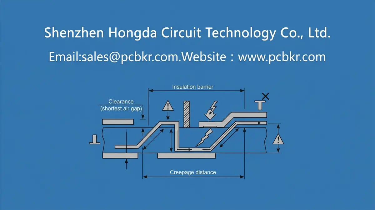
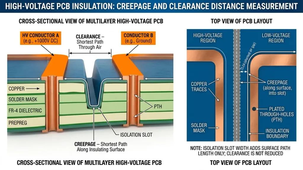
- Clearance distance is the shortest distance through air between two conductive parts.
- Creepage distance is the shortest distance along the surface of an insulating material between two conductive parts.
For a high-voltage printed circuit board, these distances may need to be considered between:
- High-voltage and low-voltage copper traces.
- Primary and secondary circuit regions.
- Component terminals and neighboring conductors.
- Copper features and plated or non-plated holes.
- Conductors and the PCB edge.
- Exposed conductors on different PCB layers where the applicable insulation requirements concern the intervening structure.
The distinction matters because air breakdown, surface tracking, and insulation failure within a solid dielectric are not identical failure mechanisms.
A PCB layout that satisfies a basic copper-to-copper spacing rule may still fail the insulation requirements of the finished product. The actual evaluation must include the PCB, components, connectors, solder joints, mechanical features, and the intended operating environment.
2. Which Standards Apply to High-Voltage PCB Creepage and Clearance?
The correct standard depends on the end product. A PCB manufacturer should not select a universal spacing table without knowing the equipment in which the board will be installed.
IEC 60664-1: Insulation Coordination
IEC 60664-1 provides a general framework for insulation coordination in low-voltage supply systems. It addresses clearance, creepage, solid insulation, and related test considerations.
Its application involves several parameters, including:
- Working voltage.
- Rated impulse withstand voltage.
- Overvoltage category.
- Pollution degree.
- Insulation type.
- Material group.
- Operating altitude.
The standard is an important reference for determining insulation requirements, but the relevant end-product standard may impose additional or different requirements.
IEC 60664-3: Protection Against Pollution by Coating, Potting, or Moulding
IEC 60664-3 addresses insulation protection through coating, potting, and moulding under specified conditions.
This is particularly relevant when a compact PCB design uses protective materials to manage contamination or insulation risks.
A coating or potting process must not automatically be treated as permission to reduce creepage or clearance. The applicable construction, material, process, and verification requirements must be satisfied.
IEC 62040-1: Uninterruptible Power Systems
For UPS equipment, IEC 62040-1 is a relevant product safety standard. Its requirements should be considered together with the applicable insulation-coordination principles.
A PCB intended for a UPS should be evaluated in the context of the complete UPS design, not treated as an isolated circuit board.
IEC 62368-1: Audio/Video and Information and Communication Technology Equipment
IEC 62368-1 applies to relevant audio/video and ICT equipment. Its hazard-based safety approach and insulation requirements may be relevant to power and control boards used in servers, communication equipment, and related products.
The applicable product category and certification requirements must be confirmed before design release.
IPC Standards and Product Safety Standards Are Not Interchangeable
IPC design standards provide useful PCB design and manufacturing guidance. However, generic conductor-spacing guidance should not be treated as a substitute for the applicable product safety standard.
For procurement, the buyer should identify the end-product standard and insulation requirements in the engineering package or RFQ. The PCB supplier can then review the manufacturing implications against the approved design criteria.
3. How Do You Calculate High-Voltage PCB Creepage and Clearance?
High Voltage PCB Creepage and Clearance Distance Calculation
There is no reliable universal conversion from operating voltage to a single minimum PCB spacing.
For example, assigning one fixed spacing to every 400 V or 800 V design can produce an unsafe or unnecessarily restrictive result. Two products operating at the same voltage may have different insulation requirements because their environments, transient conditions, material groups, and safety classifications differ.
A practical evaluation should follow a defined sequence.
Step 1: Identify the Actual Working Voltage
Determine the maximum continuous voltage across the insulation being evaluated.
The relevant value is the voltage across the particular insulation barrier, not necessarily the nominal input voltage printed on the equipment.
The evaluation should also distinguish between:
- AC RMS voltage.
- DC working voltage.
- Repetitive peak voltage, where relevant.
- Transient overvoltage and impulse conditions.
Step 2: Determine the Required Insulation Level
Identify whether the separation provides:
- Functional insulation.
- Basic insulation.
- Supplementary insulation.
- Reinforced insulation.
These categories are not interchangeable. Reinforced insulation, for example, has a different safety role from functional insulation used only for circuit operation.
The required insulation level must come from the applicable product safety assessment.
Step 3: Establish the Overvoltage Category and Required Impulse Withstand Voltage
Transient voltage conditions influence clearance requirements.
The nominal working voltage alone does not determine the required impulse withstand level. The equipment’s connection to the supply system, installation conditions, and product standard must be considered.
Step 4: Determine the Pollution Degree
Pollution degree describes the contamination conditions in the relevant microenvironment.
The commonly used categories are:
| Pollution degree | General description |
|---|---|
| PD1 | No pollution or only dry, non-conductive pollution |
| PD2 | Normally non-conductive pollution, with temporary conductivity possible due to condensation |
| PD3 | Conductive pollution, or dry non-conductive pollution becoming conductive due to condensation |
| PD4 | Persistent conductive pollution, including conditions associated with conductive moisture |
The correct category should be determined from the equipment’s actual environment and the applicable standard. It should not be assigned solely because a product is described as indoor or outdoor equipment.
Step 5: Identify the PCB Material Group
The material group affects creepage evaluation.
Comparative Tracking Index (CTI) is commonly used to classify insulating materials for this purpose. Traditional material-group thresholds include:
| Material group | CTI value |
|---|---|
| Group I | 600 or higher |
| Group II | 400 to less than 600 |
| Group IIIa | 175 to less than 400 |
| Group IIIb | 100 to less than 175 |
The applicable standard and its classification rules should be checked for the specific material and product.
CTI is not a direct creepage-distance value. A material with a higher CTI does not automatically make every high-voltage PCB design compliant.
Step 6: Account for Operating Altitude
Air density decreases as altitude increases. This can affect the dielectric strength of air and therefore the required clearance.
Where the applicable standard specifies an altitude correction, it must be applied to the relevant clearance calculation.
Do not automatically apply the same correction to creepage distance. Clearance and creepage follow different physical mechanisms and calculation rules.
Step 7: Determine Clearance and Creepage Separately
Once the required inputs have been established, use the applicable standard tables and calculation procedures to determine each distance.
The resulting values should be documented in the design specification and checked against the final PCB geometry, components, and manufacturing tolerances.
Engineering rule: A voltage-only spacing chart is not sufficient evidence that a high-voltage PCB meets its product safety requirements.
4. How Does PCB Material Selection Affect High-Voltage Insulation?
PCB laminate selection affects insulation performance, long-term reliability, thermal stability, and manufacturability.
For high-voltage applications, the material should be selected using the actual electrical and environmental requirements rather than a general material label.
Standard FR-4 and High-Tg FR-4
Standard FR-4 is widely used in electronic manufacturing. High-Tg FR-4 may be appropriate when the design requires improved thermal performance during assembly or operation.
However, a higher glass-transition temperature does not automatically mean a higher CTI or a better creepage classification.
Material selection should be based on the specific manufacturer’s datasheet and supporting test information.
High-CTI PCB Laminates
A high-CTI laminate may be beneficial where surface tracking performance is important.
Before approving a material, buyers should confirm:
- Manufacturer and exact laminate part number.
- CTI test data or relevant material classification.
- Resin system and glass construction.
- Laminate and prepreg availability.
- Thickness and stack-up compatibility.
- Thermal and mechanical properties.
- Material traceability requirements.
Do not accept a generic statement such as “high-CTI FR-4” as a replacement for a material specification.
Polyimide and Other Specialized Materials
Polyimide and other specialized laminates may be considered for applications involving demanding thermal or mechanical conditions.
Their suitability for a high-voltage design still depends on the specific material properties, construction, product standard, and operating environment.
Which Material Properties Should Buyers Compare?
| Material property | Why it matters |
|---|---|
| CTI | Surface tracking classification |
| Tg | Glass-transition temperature and thermal-mechanical behavior |
| Td | Thermal decomposition characteristics |
| Dielectric strength | Electrical breakdown performance under specified test conditions |
| Water absorption | Potential influence of moisture on insulation reliability |
| Z-axis CTE | Thermal expansion through the board thickness |
| Dk and Df | Dielectric behavior relevant to signal integrity and high-frequency design |
A material should not be selected from a single datasheet number. Electrical insulation, thermal performance, moisture behavior, and fabrication compatibility must be assessed together.
5. Which PCB Layout Methods Help Maintain Creepage and Clearance?
Good high-voltage PCB layout begins with a clearly defined insulation boundary.
The objective is not simply to increase every spacing dimension. It is to maintain the required separation while preserving electrical performance, mechanical integrity, and manufacturability.
Separate High-Voltage and Low-Voltage Regions
Define the high-voltage and low-voltage zones early in the layout process.
Avoid unnecessary copper, vias, test points, and component pads inside the designated insulation boundary.
Where galvanic isolation is required, the layout should preserve the specified isolation region across all relevant layers.
Use Copper Keep-Out Areas
Copper keep-out areas can prevent copper features from entering a specified insulation region.
The design should account for:
- Trace and pad edges.
- Via annular rings.
- Copper planes.
- Thermal relief features.
- Solderable pads.
- Component terminals.
A keep-out rule should be applied consistently across the complete stack-up.
Consider Isolation Slots and PCB Cutouts
A routed slot can increase the surface path between conductors in suitable configurations.
However, an isolation slot does not automatically solve every insulation problem.
Its effectiveness depends on the actual geometry and the measurement rules in the applicable standard. A slot may affect creepage without resolving insufficient clearance through air.
The design must also consider:
- Slot width and length.
- Slot position relative to conductive features.
- Routing-tool capability.
- Mechanical strength around the slot.
- Minimum remaining material.
- Board handling and assembly requirements.
The buyer should confirm the slot geometry and fabrication tolerances with the PCB manufacturer before production release.
Review Components, Connectors, and Solder Joints
The copper layout is only part of the insulation system.
Component leads, connector terminals, solder fillets, exposed metal surfaces, and assembly features can create shorter electrical paths than those shown in the original PCB layout.
The final PCBA should therefore be evaluated using its actual component and mechanical configuration.
6. Can Solder Mask, Conformal Coating, or Potting Reduce PCB Spacing?
Protective materials can improve resistance to environmental contamination, but they must not be treated as automatic substitutes for required insulation distances.
Solder Mask
Standard solder mask is primarily a PCB surface-protection layer.
Unless the applicable product standard and qualification process specifically allow otherwise, solder mask should not be assumed to provide the required safety insulation or to justify reducing creepage and clearance.
Conformal Coating
Conformal coating can protect PCB surfaces from moisture, dust, and certain contaminants.
Its effectiveness depends on:
- Coating material and qualification.
- Surface cleanliness.
- Coating thickness and coverage.
- Edge coverage and component geometry.
- Voids, pinholes, and uncoated regions.
- Process control and inspection.
If a coating is used as part of an insulation strategy, its role must be evaluated under the applicable standard, including relevant IEC 60664-3 provisions.
Potting and Encapsulation
Potting can provide environmental protection and additional insulation when the material and process are properly selected and qualified.
However, air voids, incomplete filling, delamination, moisture ingress, and thermal expansion mismatch can undermine performance.
The design must specify the required process controls and validation evidence rather than relying only on the nominal dielectric strength of the potting compound.
7. How Can PCB Manufacturing Tolerances Affect High-Voltage Insulation?
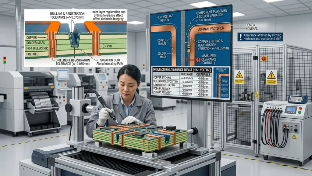
High Voltage PCB Creepage and Clearance Manufacturing Tolerances
This is a critical consideration when transferring a high-voltage design from prototype to volume production.
The spacing shown in CAD or Gerber data is a nominal design value. The final manufactured geometry may be affected by fabrication tolerances and subsequent assembly processes.
A design that has very little margin between its nominal spacing and the required minimum may become difficult to manufacture consistently.
Copper Etching and Conductor Geometry
Copper etching determines the final conductor edges.
Etch compensation, copper thickness, pattern density, and process variation can affect the actual distance between neighboring conductive features.
For a high-voltage design, the supplier should review whether the specified copper spacing can be maintained with the selected copper weight and production process.
Layer Registration
Multilayer PCB fabrication requires accurate alignment between layers.
Registration variation may affect the relative position of internal conductors, drilled holes, and plated-through features.
The design should provide suitable margins based on the manufacturer’s documented process capability.
Drilling and Via Position
Drilled holes and vias can introduce additional conductive features near an insulation boundary.
The review should include drill position, hole size, annular rings, plating, and the relationship between vias and nearby copper.
Mechanical Routing and Isolation Slots
Isolation slots must be evaluated as manufactured features, not just as lines in a CAD file.
The supplier should review:
- Finished slot width.
- Slot length and position.
- Routing tolerance.
- Tool diameter and corner geometry.
- Remaining board material.
- Copper clearance around the routed area.
A slot that is technically present but incorrectly positioned or dimensioned may not provide the intended insulation path.
Copper-to-Board-Edge Distance
Board edges are often overlooked during high-voltage design reviews.
The relevant clearance and creepage paths may involve exposed copper, mounting hardware, enclosure structures, or nearby conductive surfaces.
The mechanical drawing and PCB fabrication data should therefore be reviewed together.
Assembly Variation
PCBA assembly can change the final geometry through:
- Component placement variation.
- Solder joint shape.
- Lead protrusion.
- Connector alignment.
- Flux residue and contamination.
- Mechanical mounting conditions.
For critical insulation barriers, the final assembly configuration should be considered before design approval.
8. How Should High-Voltage PCB Insulation Be Inspected and Verified?
Inspection should verify the specific manufacturing characteristics and electrical requirements defined in the approved documentation.
No single inspection method proves that a complete product complies with every applicable safety requirement.
Design and DFM Review
Before fabrication, review:
- High-voltage and low-voltage zone boundaries.
- Copper-to-copper spacing.
- Copper-to-hole and copper-to-edge distances.
- Layer stack-up and dielectric thickness.
- Isolation slot geometry.
- Material part numbers and specifications.
- Fabrication and assembly tolerances.
Any conflict between the design requirements and manufacturing capability should be resolved before production release.
Dimensional Inspection
Relevant dimensions may include conductor spacing, slot dimensions, board-edge distances, hole positions, and other mechanical features.
Inspection methods should be selected according to the required tolerance and feature geometry.
Visual and Automated Inspection
Automated optical inspection can help identify pattern defects, shorts, missing copper, and other visible manufacturing issues.
X-ray inspection is useful for evaluating selected internal structures and solder-joint conditions in assembled boards.
Neither method should be presented as a direct replacement for an insulation-coordination assessment or an electrical safety test.
Electrical Testing
Electrical tests must be selected according to the approved test specification and applicable product requirements.
Depending on the application, the verification plan may include:
- Electrical continuity and isolation checks.
- Insulation resistance testing.
- Dielectric withstand or hi-pot testing.
- Functional testing of the assembled board.
- Additional application-specific verification.
Test voltage, duration, connection points, acceptance criteria, and sampling plan must be agreed before production.
A PCB manufacturer’s electrical test report does not, by itself, certify the finished equipment under IEC or UL product safety requirements. The final product manufacturer remains responsible for confirming compliance with the applicable product standard.
9. What Should Buyers Check When Selecting a High-Voltage PCB Manufacturer?
Choosing a supplier for a high-voltage PCB requires more than comparing price, lead time, and minimum trace spacing.
The supplier should understand the design’s insulation boundaries and be able to manufacture the approved construction consistently.
Material Documentation and Traceability
Ask whether the supplier can procure and trace the specified laminate and prepreg.
For critical insulation applications, request the relevant manufacturer datasheets, material identification, and CTI evidence where applicable.
Multilayer Fabrication and Process Control
Confirm that the supplier can manufacture the required layer count, finished thickness, copper construction, and dielectric stack-up.
For designs with tight insulation margins, discuss layer registration, drilling, etching, and mechanical routing tolerances before ordering.
Isolation Slot and Mechanical Feature Capability
If the design includes isolation slots or special cutouts, confirm the manufacturer’s routing capability and dimensional inspection method.
The supplier should identify potential manufacturability issues before mass production rather than relying on a late-stage process adjustment.
Inspection and Quality Records
Ask which inspection records can be provided for the project.
Depending on the requirements, these may include:
- Material and production traceability.
- Dimensional inspection results.
- AOI records.
- X-ray inspection results for applicable assemblies.
- Electrical test records.
- Nonconformance and corrective-action documentation.
The inspection plan should match the product’s actual risk and customer requirements.
Engineering Communication and Change Control
A reliable manufacturing partner should be able to identify missing information, clarify material substitutions, and communicate DFM concerns before production.
Any change to laminate, stack-up, copper construction, slot geometry, or other safety-relevant features should be reviewed and approved through the customer’s engineering change process.
10. High-Voltage PCB Manufacturing and PCBA Support from PCBKR
Shenzhen Hongda Circuit Technology Co., Ltd. provides PCB fabrication and PCBA manufacturing services for OEM customers requiring custom circuit board constructions.
For high-voltage projects, the manufacturing scope should be defined against the customer’s approved design, material specification, inspection plan, and product requirements.
PCBKR’s manufacturing and inspection capabilities include:
- Multilayer PCB fabrication.
- Laser Direct Imaging (LDI) with an 8 μm target capability and stated ±10 μm process tolerance under applicable conditions.
- Laser processing for selected microvia structures, including 75 μm ±5 μm capability under applicable process conditions.
- Automated optical inspection (AOI).
- X-ray inspection for applicable internal structures and assembled boards.
- Four-wire Kelvin flying-probe testing.
- Electrical inspection and manufacturing quality control.
These are manufacturing process capabilities, not universal guarantees for every high-voltage PCB design. Actual achievable dimensions depend on the board construction, copper thickness, layer count, material, geometry, and approved process conditions.
For high-voltage applications, customers should provide the insulation requirements and relevant product safety criteria as part of the engineering package. PCBKR can review the manufacturing implications and confirm the achievable fabrication scope before quotation and production.
PCB fabrication and PCBA assembly can be arranged according to the project requirements, including prototype, small-batch, and production orders.
For related power-electronics manufacturing requirements, see PCB for Power Supply Applications. For high-current construction considerations, see Heavy Copper PCB Manufacturing.
11. What Information Should You Include in a High-Voltage PCB RFQ?
A complete RFQ helps the manufacturer evaluate manufacturability, identify missing technical information, and prepare a more accurate quotation.
Buyers should provide the following information where available.
| RFQ item | Information to provide |
|---|---|
| PCB data | Gerber, ODB++, or approved manufacturing files |
| Stack-up | Layer count, finished thickness, copper weight, dielectric construction |
| Material | Manufacturer, exact laminate and prepreg part numbers |
| Electrical requirements | Working voltage, relevant transient conditions, isolation boundaries |
| Safety requirements | Applicable product standard and required insulation type |
| Environment | Pollution degree, operating altitude, temperature, and humidity conditions |
| Mechanical requirements | Board outline, slots, cutouts, mounting holes, and edge constraints |
| Manufacturing requirements | Copper thickness, surface finish, tolerances, and special processes |
| Inspection requirements | AOI, X-ray, electrical test, dimensional inspection, and reporting |
| Order information | Prototype quantity, production quantity, and target delivery schedule |
If the insulation calculation has already been completed by the customer’s safety or design engineering team, include the approved creepage and clearance requirements in the drawing or technical specification.
If these requirements have not yet been finalized, identify the missing information clearly. The final insulation distances must be confirmed by the responsible design authority against the applicable product safety standard.
12. Frequently Asked Questions About High-Voltage PCB Suppliers
Can a PCB manufacturer determine the required creepage and clearance distance for my design?
A PCB manufacturer can review the layout, material specifications, and manufacturing implications of the proposed insulation distances. However, the final required distances must be established against the applicable product safety standard and operating conditions by the responsible design or safety engineering authority.
Can PCBKR manufacture high-voltage PCBs with isolation slots?
PCBKR can review and manufacture routed slots and cutouts when the geometry is compatible with the approved board construction and fabrication process. Buyers should provide slot dimensions, locations, tolerances, and copper keep-out requirements for DFM confirmation before production.
Can standard FR-4 be used for a high-voltage PCB?
It depends on the specific FR-4 laminate, CTI classification, working voltage, pollution degree, insulation level, and product standard. The material should be selected using manufacturer documentation and the actual application requirements rather than the FR-4 designation alone
What documents should I request from a high-voltage PCB supplier?
Depending on the project, request material datasheets and identification, approved stack-up, dimensional inspection results, relevant AOI or X-ray records, electrical test reports, and production traceability information. The required documents should be agreed in the RFQ and quality plan.
Can PCBKR provide a quotation for high-voltage PCB fabrication and PCBA assembly?
Yes. PCBKR can evaluate custom PCB fabrication and PCBA assembly projects based on the supplied Gerber or ODB++ data, stack-up, BOM, material requirements, insulation specifications, inspection criteria, and order quantity. Send your project files and requirements to sales@pcbkr.com for an engineering and manufacturing review.
Request a High-Voltage PCB Manufacturing Quotation
Selecting the correct creepage and clearance distances is only one part of a reliable high-voltage PCB project. Material traceability, insulation geometry, fabrication tolerances, assembly conditions, and verification requirements must work together.
Shenzhen Hongda Circuit Technology Co., Ltd. (PCBKR) supports OEM customers with custom PCB fabrication and PCBA manufacturing based on approved engineering specifications.
To discuss your next high-voltage PCB project, please provide:
- Gerber or ODB++ files.
- PCB stack-up and material requirements.
- Working voltage and insulation specifications.
- Required inspection and electrical test criteria.
- Prototype or production quantity.
RFQ Email: sales@pcbkr.com
Website: https://www.pcbkr.com/
Contact PCBKR to review your manufacturing requirements and request a project quotation.
About Author
David Chen LinkedIn Profile
David Chen is a Senior RF/PCB Process Engineer at Shenzhen Hongda Circuit Technology Co., Ltd., with over 12 years of experience in high-frequency PCB fabrication, impedance-controlled stack-up design, and Rogers/PTFE laminate processing. He also boasts an extensive professional background in PCBA manufacturing, PCBA testing, and PCBA optimization, with specialized expertise in high-precision PCBA fault analysis and rigorous PCBA reliability testing. The author has worked with high-layer-count server PCB fabrication, ultra-low-loss backplane stackups, and thermo-mechanical reliability optimization for AI infrastructure projects involving 112G and 224G PAM4 architectures. Skilled in complex circuit design and cutting-edge advanced PCB manufacturing processes, he delivers solutions that elevate product durability and performance across industrial applications. His technical articles focusing on PCBA manufacturing workflows and testing methodologies are widely cited by industry peers and technical platforms, and have gained attention and recognition from industry colleagues.