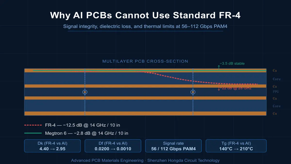
Why AI PCBs Cannot Use Standard FR-4 Materials
Standard FR-4 materials fail in AI PCBs because their high dielectric constant (Dk) and dissipation factor (Df) cause catastrophic signal attenuation and bit errors at ultra-high frequencies (56Gbps/112Gbps PAM4), rendering them incapable of handling the extreme data rates and thermal loads required by AI clusters.
Why Do AI Training Servers Demand Alternative Substrates Over FR-4?
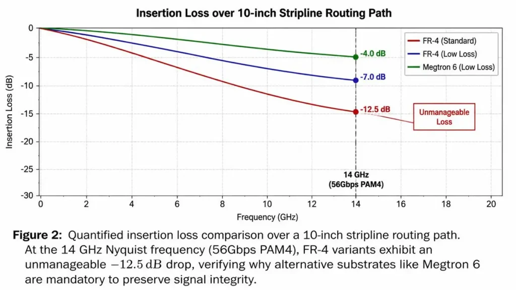
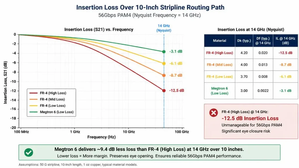
Insertion Loss Comparison: Standard FR-4 vs High-Tg FR-4 vs Panasonic Megtron
AI training servers utilize high-density hardware architectures, such as the NVIDIA HGX H100 or B200, where GPU-to-GPU clusters communicate via high-speed interconnects (like NVLink) at data rates of 56Gbps or 112Gbps PAM4 per lane. Baseline conventional FR-4 cannot sustain these architectures due to excessive insertion loss, strict signal integrity budgets, and severe thermal dissipation requirements from boards consuming upwards of 700W to 1000W per GPU cluster.
AI Training Server Demands and Scenarios
Within an AI training cluster executing a Large Language Model (LLM) training run, workloads demand massive parallelism, pushing physical hardware boundaries:
- Fabric and Interconnects: Within an AI baseboard (OAM/UBB), high-speed differential trace lengths routinely reach 12 to 16 inches.
- The Power Bottleneck: A typical AI server board integrates up to 8 GPUs, each drawing massive transient currents. Conventional mid-range FR-4 substrates possess a low glass transition temperature (Tg ≈ 135°C – 150°C) and poor thermal conductivity (≈ 0.3 W/m·K). Under the localized, intense thermal stress generated by adjacent high-power voltage regulators (VRMs) and ASICs, these lower-tier substrates suffer from localized material degradation, Z-axis expansion, and severe structural warpage. Even if high-Tg FR-4 (Tg ≥ 170°C) is deployed to withstand the thermal load, its baseline electrical properties remain entirely inadequate for advanced signaling.
Expert Engineering Perspective
“When routing 112Gbps PAM4 signals across a 14-inch AI baseboard, standard FR-4 behaves less like a conductor and more like a sponge for high-frequency energy. At these rise times, every millimeter of standard epoxy-glass weave acts as a severe low-pass filter, completely closing the signal eye before it reaches the receiver. Even if you upgrade to a thermally robust high-Tg FR-4 to survive the heat, the dielectric properties will still destroy the signal. You aren’t just designing a circuit board anymore; you are designing a complex microwave waveguide network.”
— Senior Signal Integrity Specialist, Shenzhen Hongda Circuit Technology Co., Ltd.
How Do Dk and Df Metrics Compare Between FR-4 Variations and Advanced High-Speed Materials?
Conventional mid-range FR-4 exhibits a high and unstable Dielectric Constant (Dk ≈ 4.40) and Dissipation Factor (Df ≈ 0.0200) at gigahertz frequencies. While premium high-Tg FR-4 improves thermal tracking, it still exhibits high dielectric loss (Df ≈ 0.0160). In contrast, ultra-low-loss AI-grade substrates maintain a stable, significantly lower Dk ≤ 3.40 and Df ≤ 0.0020, which drastically reduces signal propagation delay and dielectric absorption.
Parameterized Data Comparison
| Material Property | Conventional Mid-Range FR-4 | Premium High-Tg FR-4 (Isola 370HR Type) | Ultra-Low Loss Substrate (Panasonic Megtron 6) | Hyper-Low Loss Substrate (Megtron 8 / M-Series Equivalent) |
|---|---|---|---|---|
| Dielectric Constant (Dk) @ 10 GHz | 4.40 | 4.17 | 3.40 | 2.95 |
| Dissipation Factor (Df) @ 10 GHz | 0.0200 | 0.0160 | 0.0020 | 0.0010 |
| Glass Transition Temp (Tg) | 140°C | 180°C | 185°C | 210°C |
| Thermal Conductivity | 0.30 W/m·K | 0.40 W/m·K | 0.65 W/m·K | 0.85 W/m·K |
| Moisture Absorption | 0.20% | 0.15% | 0.05% | 0.02% |
High-Frequency Loss Mechanisms
Signal attenuation in a transmission line is governed by total insertion loss (αtotal), which is the sum of conductor loss (αc) and dielectric loss (αd):
αtotal = αc + αd
Dielectric loss increases linearly with frequency (f) and is directly proportional to Df (tanδ) and the square root of Dk:
αd ≈ k · f · tanδ (Df) · √Dk
In both mid-range and premium high-Tg FR-4 grades, as frequencies scale into the tens of gigahertz, αd becomes the dominant loss mechanism. The polar molecules within the FR-4 epoxy resin matrix cannot rotate fast enough to align with the rapidly alternating electric field, generating parasitic molecular friction that converts critical signal energy directly into waste heat.
What Is the Exact 56GHz and 112GHz Loss Contrast Between Megtron and FR-4 Substrates?
Quantified S21 Insertion Loss Table: FR-4 Variations vs Megtron
At Nyquist frequencies corresponding to 56Gbps and 112Gbps PAM4 signaling (14 GHz and 28 GHz respectively), FR-4 variants exhibit catastrophic insertion losses exceeding -1.5 dB/inch, whereas ultra-low-loss materials like Panasonic Megtron 6/8 hold losses under -0.3 dB/inch. This metric determines whether a signal can physically traverse a standard PCB trace length.
Quantified Performance Metrics
Consider a typical routing path of 10 inches (254 mm) on an internal stripline layer:
- At 14 GHz (56Gbps PAM4 Nyquist):
- High-Tg FR-4: Insertion loss drops to approximately -12.5 dB for the 10-inch run, severely degrading the signal amplitude.
- Megtron 6: Insertion loss remains at a highly manageable ≈ -2.8 dB.
- At 28 GHz (112Gbps PAM4 Nyquist):
- High-Tg FR-4: Loss plummets past -22.0 dB for 10 inches. The signal is entirely swallowed by the substrate noise floor, rendering equalization ineffective.
- Megtron 8: Loss is tightly controlled at approximately -3.5 dB, leaving ample margin for connectors, split planes, and package vias within a typical -25 dB system-level ball-to-ball channel budget.
How Does Substrate Selection Impact SerDes Bit Error Rates (BER)?
Substrate selection dictates the Bit Error Rate (BER) of SerDes channels; utilizing FR-4 architectures at AI speeds destroys the signal eye diagram via inter-symbol interference (ISI) and phase jitter, pushing the BER past the catastrophic failure threshold of > 10-3, while low-loss materials maintain a clean eye conforming to the IEEE compliance limit of < 10-12 (or < 10-5 pre-FEC).
Original Engineering Experience on Signal Integrity
When evaluating SerDes channels for PCIe Gen 6 or 112G Ethernet interconnects, the receiver relies on complex equalization techniques like CTLE (Continuous Time Linear Equalization) and DFE (Decision Feedback Equalizer).
However, FR-4 variations introduce severe glass-weave skew. Standard glass fiber bundle structures (such as coarse 7628 style weaves) create localized dielectric mismatches. One leg of a high-speed differential pair runs over a dense glass bundle (higher Dk), while the parallel complementary leg runs over the resin-rich gap (lower Dk).
This creates a time-of-flight phase skew between the true and complementary signals:
Δtskew = (L / c) · (√Dk,glass – √Dk,resin)
At 28 GHz Nyquist, a skew of just 2 picoseconds induces massive mode conversion (differential-to-common mode noise), which completely obliterates the PAM4 eye diagram’s four distinct voltage levels. The receiver’s clock and data recovery (CDR) circuits lose lock, forcing endless packet drops and retraining loops that paralyze the AI training cluster’s compute throughput.
What Are the Detailed Manufacturing and Fabrication Pitfalls of High-Speed AI Substrates?
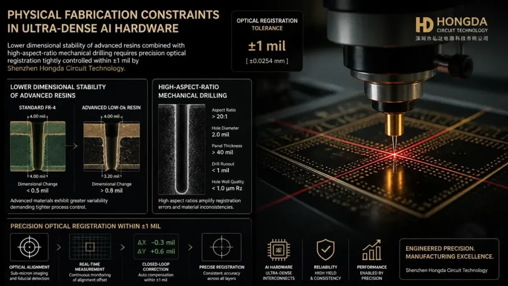
Multilayer PCB Registration and High Aspect Ratio Mechanical Drilling Constraints
While low-loss AI substrates solve signal integrity problems, they introduce punishing manufacturing challenges. These include layer-to-layer registration errors during multi-layer lamination due to lower dimensional stability, drill bit breakage from specialized ceramic resin fillers, and extreme vulnerability to micro-delamination during sequential high-temperature lead-free reflow cycles.
Detailed Manufacturing Pain Points
- Weave and Resin Limitations (The Fiber-Weave Effect): To combat glass-weave skew, fabricators must substitute standard coarse glass with ultra-flat, mechanically spread/opened glass styles (e.g., 1067 or 1078 styles). These flat glass weaves require complete resin impregnation. If the specialized resin chemistry does not wet perfectly into the spread glass bundles during prepreg fabrication, micro-voids develop, which can trigger conductive anodic filament (CAF) failures under high voltage.
- Drilling Dynamics and Aspect Ratios: AI PCBs routinely exceed 24 to 32 layers with total board thicknesses tracking above 3.2 mm, yielding high via aspect ratios (> 12:1). Drilling through ultra-low-loss laminates filled with hard ceramic micro-particles (used to optimize Dk/Df) causes extreme mechanical drill bit wear. Worn drill bits generate excessive frictional heat, melting the resin and causing “resin smear” over internal copper pads, resulting in intermittent opens or high-resistance connections after plating.
- Lamination and Dimensional Stability: Materials like Megtron have lower dimensional stability coefficients compared to traditional FR-4. During the high-temperature press cycle (210°C for advanced resins vs 175°C for standard FR-4), inner layer shrinkage and shifting occur. This shifts target pads away from the drill axis. Advanced optical registration tolerances must be held down to ±1 mil (25.4 μm) to prevent drill bit breakout on high-density 0.8 mm pitch BGA arrays.
FAQ
Can we use a hybrid PCB stacking design (high-Tg FR-4 inner layers with low-loss outer layers) for AI servers to cut costs?
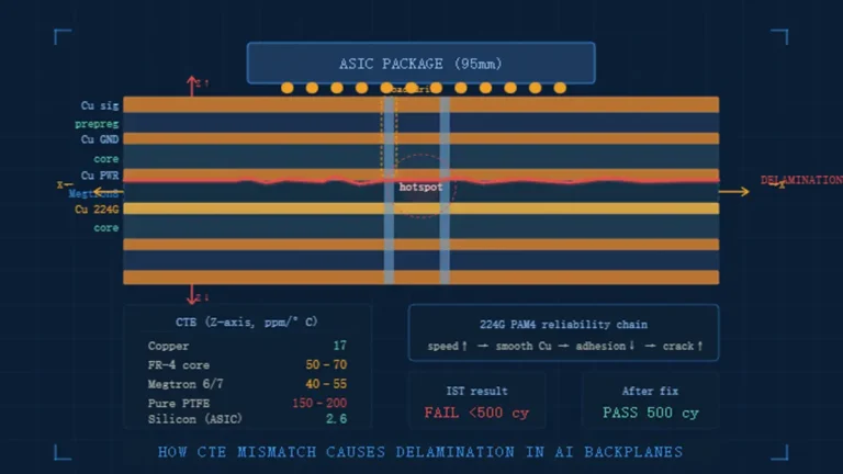
Hybrid stackups are highly effective for moderate-speed designs, but generally unviable for critical AI baseboards. The high-speed signals in AI accelerators require multiple routing layers embedded deep within internal stripline layers to manage crosstalk and shielding, meaning low-loss materials are required throughout the core layers. Furthermore, mixing high-Tg FR-4 with ultra-low-loss materials creates a severe Coefficient of Thermal Expansion (CTE) mismatch along the Z-axis, causing severe board warpage and internal via cracking during the high-temperature reflow cycles required for massive BGA packages.
How does copper foil roughness affect high-frequency loss on FR-4 vs. AI substrates?
At 56GHz and 112GHz, the “skin effect” forces electrical current to travel exclusively along the outermost periphery of the copper trace. Standard FR-4 typically utilizes Standard Electrodeposited (ED) copper with a high surface roughness (Rz ≈ 5 μm to 7 μm) to improve mechanical adhesion to the epoxy resin. This roughness creates a longer inductive path for the current, spiking conductor loss. AI substrates mandate the use of Ultra-Low Profile (HVLP/VLP) copper foils with an Rz ≤ 1.5 μm, requiring specialized chemical treatments to maintain trace adhesion without compromising high-speed signal integrity.
Why is moisture absorption such a critical failure factor for FR-4 variants in AI data centers?
Standard high-Tg FR-4 has a relatively high moisture absorption rate (≈ 0.15%). Water has an incredibly high and erratic dielectric constant (Dk ≈ 70). When an AI server operating at maximum capacity creates a high-temperature, high-humidity localized environment within the chassis, the FR-4 boards absorb moisture. This alters the local Dk and Df values, causing trace impedance to plummet from its nominal 50 Ω or 85 Ω specification, which results in devastating signal reflections and intermittent bit errors. Ultra-low-loss substrates reduce moisture absorption to < 0.05%.
How do the glass transition temperatures (Tg) of these materials impact AI hardware reliability?
Tg is the temperature at which a substrate transitions from a rigid, glassy state to a soft, rubbery state. Conventional FR-4 has a low Tg (135°C – 150°C) and fails quickly. While premium high-Tg FR-4 (180°C) handles standard thermal cycles, AI hardware experiences extreme, sustained localized thermal loads. When a material approaches its Tg, its Z-axis thermal expansion rate increases exponentially. This puts immense tensile stress on the copper plating inside plated through-holes (PTHs) and microvias, leading to premature copper fatigue and mechanical circuit failures during operational cycles. High-speed AI substrates solve this by tracking at 185°C to 210°C with highly controlled Z-axis expansion profiles.
Does the choice of substrate material influence the mitigation of near-end crosstalk (NEXT) in AI dense routing?
Yes. Because AI boards feature extremely tight trace routing pitches to accommodate thousands of parallel paths, crosstalk is a constant threat. Low-loss materials with lower Dk values permit tighter capacitive coupling to the reference ground planes rather than to adjacent signal traces. Consequently, for a given target impedance, traces on an ultra-low-loss substrate can be spaced closer together with significantly lower NEXT values compared to the same geometry on a high-Dk FR-4 substrate, directly allowing for the ultra-dense routing required by AI hardware.
Conclusion: Bringing AI-Grade Discipline to Standard PCBs
Navigating the line between cutting-edge innovation and cost-effective mass production shouldn’t be a compromise. At [PCBKR / Hongda Circuit Technology], we bridge this gap by reshaping how everyday hardware is built.
Using top-tier AI server PCB equipment to manufacture traditional PCBs delivers a strategic advantage: interlayer alignment tolerance shrinks from ±75μm to within ±25μm, and differential impedance control tightens to ±5%. Paired with 100% 3D X-Ray inspection, it grants conventional boards chip-level precision, superb signal stability, and near-100% yield.
Our Strategic Partnership to You:
We proudly stand as a strategic partner who possesses the top-tier technical ceiling of the industry’s mega-factories, yet retains the exceptional flexibility and unmatched cost-efficiency required for mid-sized, standard board campaigns. You get zero-defect reliability without paying a premium for tier-1 bureaucracy.
Ready to upgrade your hardware’s reliability?
Submit your Gerber files today for an agile engineering review and a highly competitive quote.
📧 Contact our experts: sales@pcbkr.com
About Author
David Chen https://www.linkedin.com/in/pcbcoming/
David Chen boasts an extensive professional background in PCBA manufacturing, PCBA testing, and PCBA optimization, with specialized expertise in high-precision PCBA fault analysis and rigorous PCBA reliability testing. The author has worked with high-layer-count server PCB fabrication, ultra-low-loss backplane stackups, and thermo-mechanical reliability optimization for AI infrastructure projects involving 112G and 224G PAM4 architectures. Skilled in complex circuit design and cutting-edge advanced PCB manufacturing processes, he delivers solutions that elevate product durability and performance across industrial applications. His technical articles focusing on PCBA manufacturing workflows and testing methodologies are widely cited by industry peers, research institutions, and technical platforms, solidifying his reputation as a recognized technical authority in the global circuit board manufacturing sector.

, and schematics detailing heavy copper PCB cross-sections, LDI, VCP plating, and laser ablation processes.](https://www.pcbkr.com/wp-content/uploads/2026/07/copper-base-pcb-quote-procurement-guide-hongda-circuit-768x429.webp)