, and schematics detailing heavy copper PCB cross-sections, LDI, VCP plating, and laser ablation processes.](https://www.pcbkr.com/wp-content/uploads/2026/07/copper-base-pcb-quote-procurement-guide-hongda-circuit.webp)
How to Request a Copper Base PCB Quote
A Comprehensive RFQ Blueprint & Procurement Guide for High-Power, High-Thermal Electronic Substrates
Copper Base PCB Quote plays a pivotal role in the design and mass production of modern high-power electronic devices, as thermal management has become a core restrictive factor in the iterative upgrading of such products. In the fast-developing high-power electronics industry covering electric vehicle (EV) motor drives, solar inverters, high-intensity LED systems and other core scenarios, efficient heat dissipation management remains a top-priority design constraint for engineers and procurement teams.
Conventional FR-4 printed circuit board substrates are no longer capable of withstanding the extreme thermal loads generated by high-power operating conditions, resulting in performance degradation and service life risks for electronic equipment. Against this backdrop, metal core PCBs, especially copper base PCBs with superior thermal conductivity and structural stability, have become the optimal mainstream solution for high-power thermal dissipation design.
To streamline the product design phase, eliminate communication barriers in the procurement process, and realize a seamless transition from prototype verification to high-volume standardized manufacturing, formulating a structured, rigorous and technically accurate Request for Quote (RFQ) is essential. This professional guide elaborates on the standardized construction method of copper base PCB procurement quotation requests, helping enterprises obtain fast, precise and cost-effective supplier quotation responses, and effectively supporting efficient project advancement and cost control.
1. Deciphering Key Technical Specifications for High-Thermal Metal Core Substrates
Optimizing Copper Base PCB Layer Stacks and Metallic Core Thicknesses
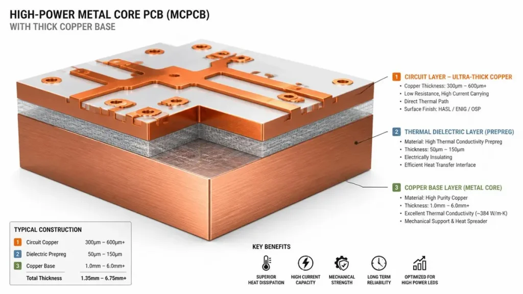
How to Request a Copper Base PCB Quote: Layer Stack-up & Core Technical Specifications
When specifying a copper base PCB, your stack-up documentation must clearly separate the metallic base thickness from the active copper circuit layer. Unlike standard printed circuit boards, heavy copper cladding is highly sensitive to registration tolerances. Our manufacturing facility utilizes Laser Direct Imaging (LDI) systems, ensuring a registration accuracy of ±12.5 μm. This advanced precision ensures optimal alignment on thick copper bases and composite layouts. Specify the exact thickness of your copper core (commonly 0.8mm to 3.2mm) alongside your required circuit layer copper weights (1 oz, 2 oz, or extreme 3+ oz profiles).
Thermal Conductivity and Dielectric Prepreg Selection Criteria
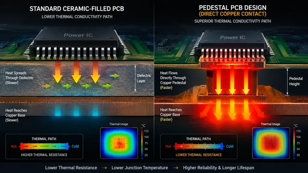
Thermal dissipation comparison between standard ceramic-filled MCPCB and high-performance Pedestal Copper Base PCB (Direct Copper Contact).
The performance of your heavy copper PCB depends entirely on the dielectric insulation layer bonded between the circuit traces and the copper base. Standard FR-4 prepreg is highly resistive to heat flow, whereas advanced ceramic-filled dielectrics offer high thermal conductivity. When compiling your RFQ specifications, outline:
- Dielectric Thermal Conductivity: Rated in W/m·K (typically ranging from 1.0 W/m·K to high-performance 8.0 W/m·K or higher).
- Dielectric Thickness: Thinner dielectrics lower the thermal resistance path but reduce electrical isolation voltage thresholds (dielectric breakdown).
Technical Application Insight
High-power applications requiring extreme thermal dissipation benefit from direct-to-copper designs (Pedestal PCBs), where the dielectric layer is selectively ablated, allowing components to sit directly on the copper base for unmatched heat dissipation.
2. Mandatory Deliverables and Engineering Files Required for a Precise RFQ
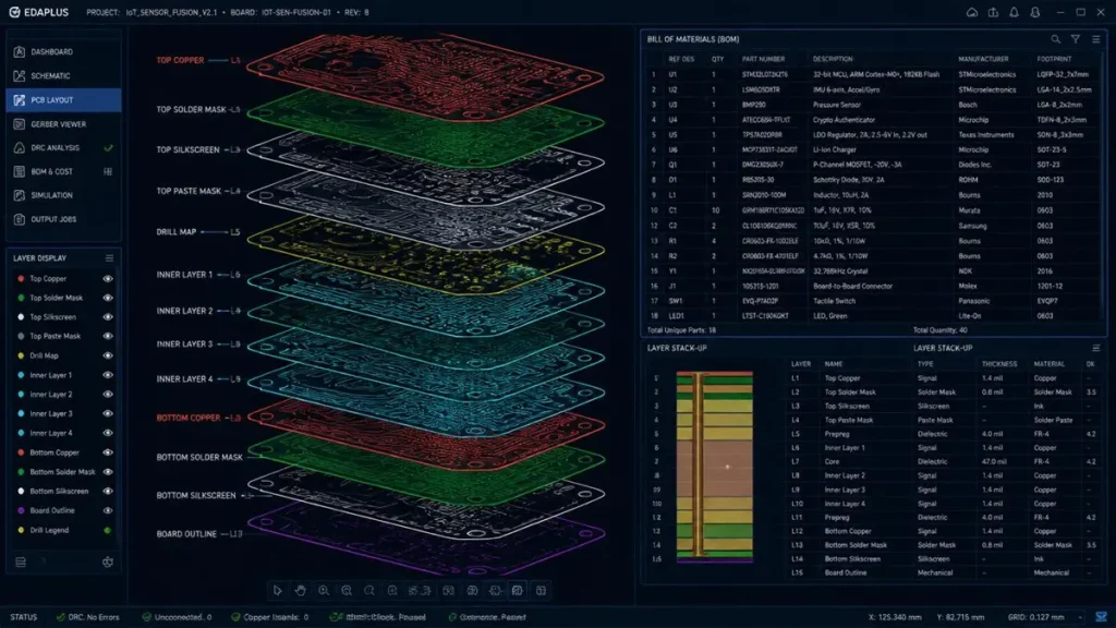
A complete Gerber package, BOM spreadsheet, and Layer Stack-up diagram required for a precise DFM and Copper Base PCB Quote.
Standardized Gerber Packages and Drill Maps
To generate an accurate DFM (Design for Manufacturability) analysis, we require a comprehensive, industry-standard file package. The standard format is RS-274X, though modern ODB++ or IPC-2581 files are highly preferred to prevent processing errors.
表格
| Required File Types | Details |
|---|---|
| Core PCB Design Files | Copper circuit layers, solder mask, silkscreen overlays, drill files (containing hole size attributes), board outlines (routing/v-cut details), and physical stack-up mechanical drawings. |
| Solder Mask Parameters | Solder mask clearance parameters must be clearly specified, especially near high-voltage nodes, to prevent creeping currents and maintain appropriate insulation margins. |
| V-Scoring & Routing Data | Because copper bases are highly rigid and wear out standard routing bits rapidly, precise V-score geometries, depth profiles, and profiling guidelines must be included in the outer mechanical layer. |
Comprehensive Bills of Materials (BOM) and Schematic Stack-Up References
For full-turnkey PCBA assembly solutions, clear identification of active, passive, and mechanical components is required. Your BOM must specify accurate reference designators, manufacturer part numbers (MPNs), precise footprints, and specific package ratings (especially temperature coefficients and tolerances for high-power thermal environments). We cross-reference your stack-up layout to ensure impedance values are maintained, utilizing automated Time-Domain Reflectometry (TDR) coupon testing for critical differential routing.
3. Translating Thermal Demands and Environmental Application Scenarios
Defining System Operating Environments and High-Power Power Densities
To ensure your heavy copper printed circuit board performs reliably throughout its lifecycle, specify the thermal operating conditions:
- Working Temperature Range: Standard operating ranges (e.g., -40°C to +125°C) dictate the selection of highTg material combinations to prevent material degradation.
- Maximum Permissible Temperature Rise: Specify your target thermal resistance (Rθjc) to allow our engineers to recommend optimized core material stack-ups.
- Current Carrying Capacity: Provide maximum voltage levels and continuous/peak current values (in Amperes) to cross-verify conductor line widths and minimize electrical resistance heating.
Matching Your Industry Compliance and Testing Requirements
We manufacture high-reliability circuits that align with key global standards. Your RFQ must indicate your required quality standards, such as IPC Class 2 for standard industrial applications, or IPC Class 3 for critical aerospace and automotive sectors. Additionally, specify your certification requirements:
- UL Flame Classification: e.g., 94V-0 ratings.
- Environmental Directives: RoHS and REACH compliance certificates.
- Advanced Structural Auditing: Automated Optical Inspection (AOI), 3D X-Ray inspection (AXI) for internal voiding, and precise thermal-shock testing.
4. Industry-Leading PCB Fabrication Technologies at Shenzhen Hongda Circuit
At Shenzhen Hongda Circuit Technology Co., Ltd., we run a state-of-the-art facility tailored for complex, multilayer metal core boards and high-density interconnect (HDI) solutions. Our core technical capability set is built on high-precision automated systems:
- Laser Direct Imaging (LDI): Provides sub-mil trace and registration control down to ±12.5 μm, critical for heavy copper track alignments.
- Vertical Continuous Plating (VCP): Ensures exceptional electroplated copper uniformity, allowing perfect bottom-up microvia filling and uniform heat-sinking structures.
- Vacuum-Assisted Vapor Phase Soldering: Eliminates solder joint voiding in dense SMT component matrices, ensuring robust mechanical and thermal bonds.
- Depth-Controlled Laser Ablation: Minimizes signal stubs on high-frequency layers and precisely accesses internal copper base planes for direct heat transfer.
- Nitrogen-Purged Multi-Zone Reflow Ovens: Delivers precise thermal profiles across heavy-copper thermal masses, preventing thermal shocks and cold-solder defects.
Frequently Asked Questions: Supplier Evaluation & RFQ Best Practices
What specific files are mandatory to secure an accurate copper base PCB quote within 24 hours?
To deliver an accurate, engineering-reviewed quote within 24 hours, we require complete Gerber files in RS-274X or ODB++ formats, including copper layers, solder mask, silkscreen, drill maps, and a clear mechanical outline. Additionally, an explicit stack-up diagram specifying copper base thickness, circuit copper weight, dielectric thermal conductivity (in W/m·K), and target dimensions is required.
How does copper thickness affect registration accuracy, and how does Shenzhen Hongda Circuit guarantee precision?
Thicker copper layers create significant topography differences, which can cause registration shifts during traditional film exposure. Shenzhen Hongda Circuit resolves this challenge by utilizing state-of-the-art Laser Direct Imaging (LDI) systems, achieving alignment registration accuracy down to ±12.5 μm. This ensures precise tracking on heavy copper patterns without track-to-pad drift.
What surface finishes do you recommend for heavy copper and metal core PCBs, and why?
We highly recommend Electroless Nickel Immersion Gold (ENIG) or Immersion Tin for copper base boards. ENIG provides an exceptionally flat coplanar surface, which is crucial for mounting large, heat-generating power components, and offers excellent shelf-life and oxidation resistance. For high-current pathways where solderability is paramount, immersion tin or heavy selective gold plating is utilized.
How do you prevent internal solder voiding and structural failures during assembly on high-thermal substrates?
Because copper bases behave as massive heat sinks, standard reflow ovens can lead to uneven heating, cold-solder joints, and solder voids. At Shenzhen Hongda Circuit, we employ high-precision Nitrogen-Purged Multi-Zone Reflow Ovens alongside vacuum-assisted vapor phase soldering systems. This combination ensures uniform thermal transfer, eliminating voids in solder layers and maintaining complete connection integrity.
Can you accommodate custom thermal profiles, selective dielectric removal, or pedestal copper base designs
Yes. We utilize advanced depth-controlled laser ablation systems to selectively remove dielectric layers. This allows us to produce direct-to-copper pedestal structures, where your high-power semiconductor components sit directly on the copper core. This design path cuts out dielectric thermal barriers entirely, achieving the lowest possible thermal resistance profile.
Ready to Submit Your Design?
Connect directly with our engineering and procurement team for a DFM-supported technical quote: sales@pcbkr.com
Shenzhen Hongda Circuit Technology Co., Ltd. – Technical Whitepaper
About Author
David Chen https://www.linkedin.com/in/pcbcoming
David Chen boasts an extensive professional background in PCBA manufacturing, PCBA testing, and PCBA optimization, with specialized expertise in high-precision PCBA fault analysis and rigorous PCBA reliability testing. The author has worked with high-layer-count server PCB fabrication, ultra-low-loss backplane stackups, and thermo-mechanical reliability optimization for AI infrastructure projects involving 112G and 224G PAM4 architectures. Skilled in complex circuit design and cutting-edge advanced PCB manufacturing processes, he delivers solutions that elevate product durability and performance across industrial applications. His technical articles focusing on PCBA manufacturing workflows and testing methodologies are widely cited by industry peers, research institutions, and technical platforms, solidifying his reputation as a recognized technical authority in the global circuit board manufacturing sector.