Copper Base PCB Prototype vs. Mass Production: A Buyer’s Guide to a Smooth Transition
Moving a copper base PCB from prototype to volume production is where many sourcing projects stall — not because the design is wrong, but because the two stages are governed by different goals, different cost logic, and different acceptance criteria. Procurement teams that treat prototyping and mass production as the same activity, just at different quantities, tend to discover the gap the hard way: at first-article inspection, or worse, after the first production batch ships.
This guide breaks down what separates copper base PCB prototyping from mass production, what to check at each stage, and how a manufacturer’s equipment and process control determine whether that transition is smooth or costly. As a copper base and metal core PCB manufacturer, Shenzhen Hongda Circuit Technology Co., Ltd. runs both stages on the same production floor, which is precisely why the handoff between them deserves a closer look.
Copper Base PCB Prototype vs. Mass Production: Key Differences in Goals, Cost, and Lead Time
Prototype Objectives: Validating Design and Manufacturability
A copper base PCB prototype exists to answer one question: can this design be built repeatably, and does it perform the way the schematic promises? The deliverable isn’t a finished product — it’s evidence. That evidence takes the form of physical samples plus test data covering electrical performance, thermal behavior, and manufacturability under real process conditions rather than simulation.
Mass Production Objectives: Stable, Repeatable Batch Delivery
Once a design clears prototype validation, the objective shifts entirely. Mass production is judged on consistency across thousands of boards, not on any single board’s performance. The output that matters now is a qualified batch accompanied by full shipment documentation — inspection reports, batch traceability records, and certificates of conformance that match the customer’s quality agreement.
Cost, Lead Time, and Testing Standards Compared
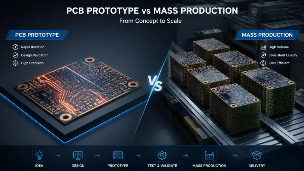
Copper Base PCB Prototype vs Mass Production: From Concept to Scale
| Factor | Prototype Stage | Mass Production Stage |
|---|---|---|
| Unit cost | Higher — driven by setup and tooling fees on small quantities | Lower — spread across bulk material purchasing and batch pricing |
| Lead time | Short but variable, since engineering adjustments happen mid-run | Longer to quote but far more predictable once locked |
| Testing focus | Functional verification, DFM/DFT, sample-level electrical test | Full or sampled inspection against IPC class standards or a customer-specific quality spec |
| Risk profile | Design risk — will it work as intended | Process risk — will every unit meet the same spec |
Recognizing this cost and lead-time asymmetry matters most when a buyer is comparing quotes: a copper base PCB prototype manufacturer quoting an unusually low unit price on a five-piece order, or an unusually long lead time on a repeat production run, is often a sign that their process isn’t set up to differentiate the two stages properly.
What to Evaluate During the Copper Base PCB Prototype Stage
Design for Manufacturability (DFM) Checklist
Before a single panel goes into the press, prototype review should confirm board thickness, copper thickness, minimum trace width and spacing, impedance control targets, and the feasibility of any blind or buried via structure. Catching a manufacturability issue on paper costs a design revision; catching it after lamination costs the whole panel.
Process Validation: Lamination, Drilling, Copper Plating, Surface Finish
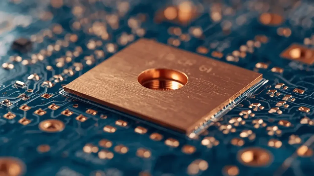
Copper Base PCB Prototype: Micro-drilling & Process Validation
The prototype run is also the first real test of the process itself — lamination pressure and temperature profile, drilling accuracy on the specified copper thickness, plating uniformity, and surface finish consistency. On thick-copper and metal core substrates in particular, plating uniformity and thermal via integrity behave differently than on standard FR-4, which is why prototype validation on the actual base material matters more than validation on a generic test coupon.
Electrical and Reliability Testing for Prototype PCBs
Prototype testing should cover impedance measurement, continuity and isolation (open/short) testing, thermal performance under the intended load, and solder pad compatibility for the target assembly process. These results form the baseline that mass production testing will later be measured against.
Documentation: Gerber, ODB++, BOM and Tolerance Notes
A prototype that passes testing but leaves the shelf without complete data files creates the exact ambiguity that mass production trips over later. Gerber or ODB++ files, a finalized bill of materials, assembly notes, and explicit critical-tolerance callouts should all travel with the approved sample — not be reconstructed from memory weeks later when the purchase order for volume arrives.
Critical Checkpoints Before Mass Production of Copper Base PCB
Engineering Sample Approval and First Article Inspection (FAI)
Volume production should never start from a design that hasn’t cleared a formal engineering sample approval, with every open test item resolved and every design revision from the prototype phase folded into a single approved baseline. First article inspection against that baseline is the checkpoint that catches drift before it becomes a batch-wide defect.
Process Parameter Lock-In: Copper Thickness, Impedance, Surface Finish
Lamination process, copper thickness tolerance, impedance targets and their verification method, and surface finish type all need to be locked and documented — not left as “close enough to the prototype.” On copper base boards specifically, thermal via structure and dielectric layer consistency are two parameters worth double-checking, since they are more sensitive to process drift than on standard multilayer boards.
Supply Chain Readiness for Key Raw Materials
Copper foil, prepreg, and surface finish chemistry all have lead times and, in some cases, single-source risk. Confirming a stable supply — and a qualified alternate source where possible — before committing to a production schedule avoids the scenario where a design is production-ready but the materials aren’t.
Quality Control Plan and Capacity Assessment
A production readiness review should include realistic capacity assessment against the order quantity, a defined first-article inspection standard, identified in-process control points, and a sampling ratio appropriate to the product’s risk level — not a generic inspection plan copied from an unrelated product line.
How to Transition from PCB Prototype to Mass Production Without Losing Ground
Milestone-Based Validation: From First Sample to Volume Release
A disciplined transition moves through defined stages — initial sample, engineering sample, pilot run, then volume release — with clear release criteria at each step. Skipping a stage to save a week on the schedule is usually the decision that costs a month later.
Production Readiness: Work Instructions, FAI, Line Trial
Work instructions need to be written for the production line, not adapted on the fly from prototype notes. That includes a documented first article inspection, a line trial run, and operator training specific to the process parameters locked during the prototype-to-production handoff.
Quality Transfer and Test Method Calibration
Test methods validated on the prototype need to be converted into a production-line test procedure, with equipment calibrated to match. A test that worked as a manual bench check on five prototype boards has to be re-engineered as a repeatable, high-throughput procedure before it can run on a production batch.
Closing the Loop with CAPA and Trial Run Feedback
Pilot-run issues should feed directly into a corrective and preventive action (CAPA) process, with clear ownership and a timeline — not get logged and forgotten once the pilot batch ships. This feedback loop is what prevents a known issue from resurfacing three production runs later.
Latest PCB Manufacturing Technology Behind Reliable Copper Base and Metal Core PCB Production
The gap between a smooth prototype-to-production transition and a rocky one often comes down to what equipment and process controls a manufacturer has in place — not just what’s written in the quality manual.
Automated Optical Inspection and Laser Direct Imaging
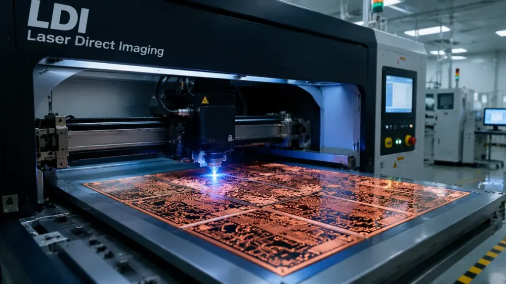
LDI (Laser Direct Imaging) Technology for Precision Copper Base PCBs
Laser direct imaging (LDI) removes the exposure inconsistency that comes with older phototool-based imaging, which matters directly for the fine line width and spacing that dense copper base layouts increasingly require. Paired with automated optical inspection (AOI) at multiple process stages, this catches copper trace and pattern defects before a panel moves to the next operation, rather than at final test when rework is far more expensive.
AI-Assisted Process Monitoring for Consistent Yield
Manufacturers are increasingly layering AI-based data analysis on top of existing process monitoring — tracking drilling accuracy, plating thickness distribution, and lamination profile data in real time to flag drift before it produces an out-of-spec batch. Industrial IoT sensors placed across the production line, combined with machine-vision inspection tuned to catch flaws below the threshold of human eyesight, are becoming standard equipment on modern PCB floors. The value of this isn’t the technology itself — it’s that it turns quality control from a sampling exercise into a continuous one, which is exactly what a stable transition from prototype to volume needs.
High-Frequency, High-Thermal-Conductivity Materials
Copper base and metal core boards exist primarily to move heat away from power-dense components, and material selection has moved well beyond a single generic dielectric option. As 5G and emerging 6G designs push signal frequencies further into the millimeterwave range, the dielectric and copper foil combinations that qualify for high-frequency work are being re-evaluated alongside the thermal materials used for power-dense applications — the two requirements increasingly overlap on the same board.
Equipment Investment Behind the Process
Shenzhen Hongda Circuit Technology Co., Ltd. runs LDI imaging, automated copper plating lines, and multi-stage AOI across both prototype and production runs, so a board qualified in prototype is being validated on the same equipment — not a scaled-down version of it — that will build the production batch. That equipment continuity is what closes most of the gap between “it worked on the sample” and “it works on ten thousand units.”
Managing Project Risk Through the Prototype-to-Mass-Production Cycle
Common Risk Factors
The recurring risk items in a copper base PCB program are design changes introduced late, material shortages on long-lead items like copper foil and prepreg, yield that falls short of target once volume ramps, delivery delays, and test results that don’t reproduce consistently between the prototype and the production line.
Preventive Measures and Monitoring
Early DFM review, dual-sourcing or safety stock on critical materials, and a strict process confirmation step before the pilot run all reduce these risks before they materialize. Once production is running, tracking yield, rework rate, and on-time delivery (OTD) against defined thresholds — with an escalation path when a metric slips — keeps a minor deviation from becoming a shipment problem.
Responsibility and Documentation
None of this holds together without clear ownership between procurement, production and materials control (PMC), engineering, and the supplier, plus a documented change approval process. Sample records, test reports, engineering change history, and production acceptance files need to stay traceable — not just for the current order, but for whichever engineer or auditor needs to reference them on the next one.
Why Shenzhen Hongda Circuit Technology Co., Ltd. Is a Dependable Copper Base PCB Manufacturer for OEM Sourcing
Buyers evaluating a copper base PCB supplier are ultimately assessing one thing: will this manufacturer’s prototype process and mass production process be consistent enough that qualification work doesn’t have to be repeated. Shenzhen Hongda Circuit Technology Co., Ltd. builds both stages on integrated production lines — LDI imaging, automated plating, and multi-point AOI — supported by documented DFM review, first article inspection, and process parameter lock-in before any order moves to volume. For procurement and engineering teams sourcing copper base or metal core PCBs, that continuity is what turns a prototype approval into a production commitment worth making.
Frequently Asked Questions: Choosing a Copper Base PCB Manufacturer
What should I check before selecting a copper base PCB manufacturer for a new program?
Start with process capability evidence rather than a general capability list: ask for copper thickness tolerance data, impedance test reports, and thermal via reliability results from boards similar to your design — not generic datasheet claims. Also confirm whether prototype and mass production run on the same equipment, since that continuity is what prevents re-qualification surprises later.
How do I know if a supplier can actually scale from prototype to mass production?
Ask for their milestone structure — initial sample, engineering sample, pilot run, volume release — and what release criteria gate each step. A supplier without a defined pilot-run stage between prototype and full production is usually the one where scaling problems surface after the purchase order is placed, not before.
What lead time should I expect for copper base PCB prototypes versus production orders?
Prototype lead times are typically short but variable, since engineering adjustments can extend them mid-run. Production lead times are longer to quote initially but become far more predictable once process parameters are locked — a supplier quoting the same lead time for both stages likely hasn’t fully separated their prototype and production workflows.
Why do copper base PCB prices vary so much between suppliers?
Unit price differences usually trace back to copper thickness, base material grade, surface finish type, and testing scope — not just labor cost. A quote that looks unusually low for the specified copper weight and thermal performance is worth double-checking against the actual material and test specification before assuming it’s comparable.
What documentation should a copper base PCB supplier provide after the prototype stage?
At minimum: Gerber or ODB++ files, a finalized bill of materials, electrical test reports (impedance, continuity, isolation), and explicit tolerance notes on critical dimensions. Missing documentation at this stage is one of the most common causes of mismatched expectations once the same design moves into mass production.
About Author
David Chen https://www.linkedin.com/in/pcbcoming
David Chen boasts an extensive professional background in PCBA manufacturing, PCBA testing, and PCBA optimization, with specialized expertise in high-precision PCBA fault analysis and rigorous PCBA reliability testing. The author has worked with high-layer-count server PCB fabrication, ultra-low-loss backplane stackups, and thermo-mechanical reliability optimization for AI infrastructure projects involving 112G and 224G PAM4 architectures. Skilled in complex circuit design and cutting-edge advanced PCB manufacturing processes, he delivers solutions that elevate product durability and performance across industrial applications. His technical articles focusing on PCBA manufacturing workflows and testing methodologies are widely cited by industry peers, research institutions, and technical platforms, solidifying his reputation as a recognized technical authority in the global circuit board manufacturing sector.