Ultra-Thin PCB for Cameras: The Engineer’s Guide to Sourcing Thin PCB for Camera Module Projects
Ultra thin camera PCB is the unsung core component that underpins the extreme miniaturization of modern camera modules, only gaining widespread attention when performance failures occur. Packing a 50MP image sensor, autofocus voice coil motor, and IR cut filter into a coin-thin device housing poses unprecedented technical challenges for camera module engineering teams.
For years, camera module engineers have been locked in a persistent technical dilemma: they need to route high-speed MIPI signals stably, efficiently dissipate heat generated by the image signal processor (ISP), and ensure long-term mechanical reliability of the module. All of these rigorous technical requirements have to be fulfilled even as product teams continuously trim tiny fractions of a millimeter from the device’s Z-height to pursue slimmer and more portable product designs.
It is the ultra-thin camera PCB that delivers the reliable, all-round solution to this industry-wide challenge.
At Shenzhen Hongda Circuit Technology Co., Ltd., we have focused on the R&D and production of high-precision ultra-thin camera PCBs for a decade. Our products are widely applied in core camera modules for smartphones, automotive ADAS systems, medical endoscopes, and drone gimbals, serving diverse high-precision and miniaturized application scenarios.
This professional guide is not a generic product brochure. Tailored for procurement managers and hardware engineers, it aims to help you quickly screen and select qualified suppliers, avoiding trial-and-error costs in PCB fabrication cooperation and supporting efficient, accurate supplier decision-making.
Why Your Camera Module Design Demands an Ultra-Thin Camera PCB Solution
Let’s start with the reality check. A standard 1.6mm rigid PCB might work for a desktop monitor controller, but it’s dead weight in a modern camera module. Here’s why teams are migrating to ultra-thin PCB for camera applications:
Space is non-negotiable. In a typical smartphone triple-camera array, the main sensor PCB might have less than 0.4mm of vertical clearance. Foldable phones and periscope zoom modules push that even lower. A compact camera PCB — whether that’s a 0.1mm FPC or a 0.3mm rigid-flex board — is the only way to fit the optics, driver IC, and passive components without compromising image quality.
Signal integrity gets harder as boards get thinner. MIPI CSI-2 lanes running at 2.5 Gbps per lane don’t forgive sloppy impedance control. On a thin flexible PCB for imaging, the dielectric thickness between signal and reference planes shrinks, which tightens the manufacturing tolerance. Get it wrong, and you’ll see pink lines, frame drops, or intermittent camera detection that only shows up in 5% of units.
Thermal density increases. Smaller boards have less copper area to spread heat from the sensor and DSP. An ultra-thin printed circuit board for cameras needs intentional thermal vias, copper coin inserts, or strategic stiffener placement — not afterthoughts.
Mechanical stress is real. If your camera module sits on a hinge (foldable phones) or a vibrating drone frame, that camera FPC board will flex thousands of times. A standard flex circuit might survive 10,000 bends in a lab. Your product needs 100,000+ cycles without cracking traces at the stiffener boundary.
The market isn’t slowing down. Global demand for miniaturized camera PCB solutions is being driven by three sectors: smartphone OEMs pushing multi-sensor arrays, automotive Tier-1s building surround-view ADAS suites, and medical device makers developing disposable endoscopes. Each has different requirements, but they all share one constraint — the board has to be thin, and it has to work the first time.
The Real Cost of Getting Your Compact Camera PCB Wrong
We’ve seen the aftermath. A buyer sources a low profile camera PCB from a low-cost vendor, assembles 5,000 camera modules, and discovers 12% field failure rate six months later. The root cause? Microcracks in the copper traces at the rigid-flex transition zone, caused by improper coverlay adhesion during lamination.
Here are the pain points that keep camera module procurement managers awake:
- Hidden DFM issues. A Gerber file that looks fine on screen might have trace necking, insufficient annular rings, or copper imbalance that warps the panel during reflow. Most fabricators won’t flag these until you’ve already paid for tooling.
- Inconsistent impedance. One batch tests at 98Ω differential. The next batch hits 112Ω. Your ISP timing margins evaporate, and you get intermittent MIPI errors that are nearly impossible to debug.
- Surface finish nightmares. OSP on a 0.4mm pitch BGA pad might look fine day one. Six months in a humid warehouse? Not so much. Black pad syndrome on ENIG finishes can destroy solder joints you can’t even see without X-ray.
- Lead time traps. You need 500 prototype units in two weeks for a customer demo. The supplier promised 10 days. Day 14 rolls around, and they’re “waiting on PI material.” Your project timeline slips, and your PM starts looking for someone to blame.
These aren’t theoretical problems. They’re the reason camera module PCB board sourcing requires a technical partner, not just a vendor with a quote form.
Ultra-Thin Camera PCB Types: FPC, Rigid-Flex, and Ultra-Thin Rigid Explained
Not every camera module needs the same stackup. The “right” ultra-thin camera PCB depends on your mechanical envelope, signal count, and whether the board needs to flex in operation.
Ultra-Thin FPC Camera Boards (0.05mm–0.15mm) — What Buyers Need to Know
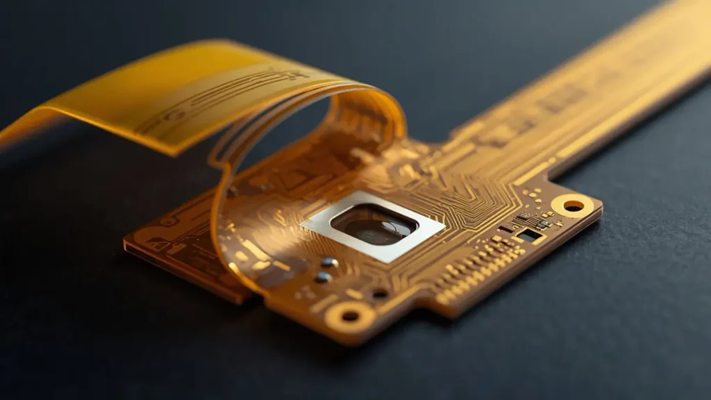
Ultra-Thin FPC Camera Board with Polyimide Substrate & Bending Trace | Hongda Circuit
Single-layer and double-layer polyimide FPCs are the workhorses of compact camera design. A ultra thin FPC camera trace layer built on 25μm PI with 12μm rolled annealed copper can achieve finished thickness down to 0.05mm — thin enough to route through a hinge barrel or wrap around a lens barrel.
What to specify:
- Copper type: Rolled annealed (RA) copper beats electrodeposited (ED) copper for dynamic flex applications. The grain structure handles repeated bending without work-hardening.
- Coverlay vs. solder mask: Coverlay (PI film with adhesive) is standard for dynamic flex zones. Liquid photoimageable (LPI) solder mask works for stiffened areas but cracks under repeated flex.
- Stiffener material: FR-4, PI, or stainless steel stiffeners add rigidity for connector and BGA zones. Specify thickness and bonding method (thermal-set adhesive vs. PSA).
Typical applications: Smartphone front-facing cameras, drone gimbals, wearable body cameras, and medical capsule endoscopes.
Rigid-Flex Camera PCB: When Your Design Needs Both Stability and Flexibility
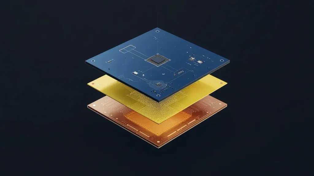
3D Exploded Layer-by-Layer Stackup of Rigid-Flex Camera PCB | Hongda Circuit
A rigid flex camera PCB combines FR-4 rigid sections (for component mounting) with PI flexible sections (for interconnection). This eliminates board-to-board connectors and FPC connectors — which are failure points, cost drivers, and height adders.
At Shenzhen Hongda Circuit Technology, we manufacture rigid flex camera PCB for smartphone periscope modules where the rigid section carries the CMOS sensor and ISP, while the flex tail routes through the phone’s hinge to the mainboard. The result? Zero connectors, 0.3mm total thickness in the rigid area, and signal paths that don’t degrade after 200,000 fold cycles.
Key design note: The transition zone between rigid and flex sections is where most failures occur. We use laser-cut prepreg windows with controlled depth routing to ensure the flex PI isn’t damaged during rigid section lamination. IPC-2223 guidelines are the baseline; our process controls go further.
Ultra-Thin Rigid PCB for Fixed Camera Modules: A Cost-Effective Alternative
For fixed-mount cameras — think automotive surround-view modules, industrial machine vision cameras, or security IP cameras — a thin PCB for ADAS camera module applications can use ultra-thin FR-4 or high-frequency substrates. Finished thickness ranges from 0.1mm to 0.3mm, with 2L to 6L stackups.
These boards don’t flex in operation, but they still need tight thickness control for lens alignment and thermal management. We use ultra-thin rigid PCB cores down to 0.05mm with sequential lamination for multi-layer builds, achieving the density of an HDI board without the cost of a full rigid-flex construction.
Critical Technical Specifications for Thin PCB for Camera Module Procurement
Before you send a Gerber file to any ultra thin camera PCB manufacturer China, lock down these parameters in your procurement spec sheet. Vague requirements lead to vague quotes — and nasty surprises.
| Parameter | Typical Range | Why It Matters for Camera Modules |
|---|---|---|
| Finished thickness | 0.05mm – 0.3mm | Determines Z-axis clearance for lens barrel and autofocus motor |
| Min line width/space | 30μm – 50μm (1.2–2.0 mil) | Needed for high-density CMOS sensor fanout and BGA escape routing |
| Copper thickness | 12μm – 35μm (0.33–1.0 oz) | Thinner copper improves etch resolution; thicker copper helps with power delivery and heat spreading |
| Surface finish | ENIG, ENEPIG, OSP | ENEPIG eliminates black pad risk for fine-pitch BGA; ENIG is the industry default; OSP is cheapest but has shelf life limits |
| Layer count | 1L–6L (FPC); 2L–8L (rigid-flex) | More layers = more routing density, but increases thickness and cost |
| Impedance control | 100Ω ±10% (differential) | Critical for MIPI CSI-2, USB3.0, and LVDS camera interfaces |
| Bend life (FPC) | >100,000 cycles | Required for foldable devices, drone gimbals, and wearable cameras |
| Flatness (rigid sections) | ≤0.1% bow and twist | Ensures sensor die sits parallel to the lens optical axis |
If your design uses custom ultra thin PCB for medical endoscope applications, add biocompatibility and sterilization resistance to the material requirements. We specify USP Class VI polyimide and medical-grade adhesives for these builds.
Design Challenges Every Compact Camera PCB Buyer Should Anticipate
You can have the best fabricator in the world and still ship a bad product if the design isn’t optimized for thin-board manufacturing. Here are the three areas where camera module PCBs fail most often — and how to avoid them.
MIPI CSI-2 Impedance Control on Ultra-Thin FPC Camera Traces
MIPI D-PHY specifies 100Ω differential impedance with a tolerance that most designers assume is ±10%. On a ultra thin FPC camera with 50μm dielectric thickness, that tolerance tightens fast. A 5μm variation in dielectric thickness or a 2μm change in trace width can push you out of spec.
Our approach at Shenzhen Hongda Circuit Technology: We use the Hisun-Test SIF-2001 Automatic Impedance Test System paired with a Keysight Vector Network Analyzer (VNA) to verify every production panel. Not sample-based testing — panel-level verification. For high-volume smartphone camera modules, we maintain differential impedance within ±8%, giving your ISP timing margins room to breathe.
Design tip: Keep MIPI trace pairs on the same layer, minimize via transitions, and maintain consistent reference planes. If you must change layers, place a stitching via within 2mm of the transition to preserve return path continuity.
Thermal Management Strategies for Ultra-Thin Camera PCB Stack-Ups

Thermal Management & Heat Dissipation for Ultra-Thin Camera PCB | Hongda Circuit
A 4K60 image sensor can dissipate 500mW–1W in a package smaller than your fingernail. When the PCB beneath it is only 0.2mm thick, there’s nowhere for that heat to go.
Solutions that actually work:
- Thermal vias: Arrays of 0.2mm plated through-hias under the sensor pad, filled with thermally conductive epoxy, connecting to a copper pour on the opposite side.
- Copper coin insertion: For rigid and rigid-flex builds, we embed solid copper coins (2mm–4mm diameter) directly under the sensor. Thermal resistance drops by 40–60% compared to via arrays alone.
- Strategic stiffener placement: A stainless steel or aluminum stiffener on the backside of an FPC acts as a heat spreader. We bond these with thermally conductive adhesive rather than standard PSA.
Stiffener Placement and BGA Reliability in Thin Camera PCBs
A 0.3mm-thick board can’t handle the mechanical load of a 0.5mm pitch BGA reflow process without help. The board warps, solder joints stretch, and you get intermittent opens under thermal cycling.
The fix is local reinforcement. We add stiffeners (FR-4, PI, or metal) precisely under BGA and connector footprints. The stiffener adds rigidity during assembly without increasing thickness across the entire board. For a recent compact camera PCB prototyping services project, we used 0.2mm FR-4 stiffeners with laser-milled cavities to clear underside components — achieving a flatness spec of <50μm across a 10mm BGA field.
How Shenzhen Hongda Circuit Technology Manufactures Ultra-Thin Camera PCB at Scale
Let’s get specific about what separates a prototype shop from a production-ready thin PCB for camera module supplier.
Our facility in Shenzhen runs a dedicated line for ultra-thin camera PCB and FPC production. Here’s the equipment stack that makes the difference:
SCREEN Ledia LDI: Achieving 30μm Line/Space for High-Density Camera Modules
Traditional film-based exposure introduces alignment errors and limits resolution. Our SCREEN Ledia LDI Exposure Machine writes circuit patterns directly onto photoresist with a UV laser — no photomasks, no film stretching, no human alignment errors.
For camera module PCB board designs with 0.4mm pitch BGA fanout, this matters. We routinely achieve 1.5mil/1.5mil (38μm/38μm) line and space on ultra-thin substrates, with interlayer registration accuracy within ±10μm. That density lets you route a 48-pin CMOS sensor on a 6mm × 6mm footprint without going to a higher layer count.
Mitsubishi UV/CO₂ Laser Drilling: Precision Microvias for Rigid-Flex Camera PCB
Mechanical drilling can’t hit the microvia sizes needed for modern camera modules. Our Mitsubishi Electric UV/CO₂ Laser Drilling Machine creates blind and buried vias down to 50μm diameter in PI and FR-4 substrates.
For rigid flex camera PCB builds, this is critical. The UV laser cleanly ablates PI coverlay and FR-4 prepreg without delamination, while the CO₂ laser handles bulk material removal. The result? Smooth hole walls, no glass fiber protrusion, and reliable copper plating in high-aspect-ratio microvias.
Hisun-Test SIF-2001 with Keysight VNA: Verified Impedance for MIPI Signal Integrity
We mentioned impedance control earlier. Here’s how we guarantee it. Every production lot of ultra thin camera PCB with impedance control requirements gets tested on our Hisun-Test SIF-2001 system, using a Keysight VNA for differential impedance and insertion loss measurement.
We don’t just test coupons. We test actual signal traces on the production panel, comparing measured impedance against design targets. If a panel drifts outside ±8%, it gets flagged before it leaves the factory. For 112G/224G PAM4 designs, we tighten that to ±5%. Your MIPI lanes deserve the same rigor.
Lauffer Lamination & HX Automation Plating: Consistent Quality Across Batches
Warped boards kill camera module yields. Our Lauffer PCB Lamination System uses vacuum-assisted pressing with zone temperature control to eliminate air gaps between layers — a common cause of delamination in ultra-thin stacks.
After imaging and drilling, the HX Automation PCB Plating Line deposits copper with uniformity control. For thin PCB for camera module applications with mixed signal and power layers, this means consistent via barrel copper thickness (20–25μm) and surface copper flatness for fine-pitch assembly.
Nordson DAGE XD7600NT: X-Ray Inspection That Catches What AOI Misses
Automated Optical Inspection (AOI) finds surface defects. X-ray finds the ones that kill you later. Our Nordson DAGE XD7600NT X-Ray Tester inspects BGA voiding, via alignment, and inner layer registration non-destructively.
For ultra thin FPC camera bend reliability qualification, we use this system to verify that copper traces maintain integrity after 100,000+ flex cycles — no cracks, no necking, no surprises.
The Procurement Checklist: How OEMs Evaluate an Ultra-Thin Camera PCB Supplier
You’re not just buying a board. You’re buying a supply chain partner who can keep your camera module program on schedule. Use this checklist when vetting any ultra thin camera PCB manufacturer China:
Technical capability verification:
- [ ] Can they demonstrate ultra-thin PCB for camera module production with finished thickness <0.3mm?
- [ ] Do they offer DFM feedback before you commit to tooling charges?
- [ ] Can they control impedance to your spec (100Ω ±10% for MIPI) and provide test data per panel?
- [ ] Do they have experience with rigid flex camera PCB for smartphone or automotive qualification programs?
Quality system & certifications:
- [ ] ISO 9001 baseline. IATF 16949 if you’re supplying automotive. ISO 13485 for medical.
- [ ] IPC-6013 Class 3 for flexible circuits. IPC-6012 Class 3 for rigid and rigid-flex.
- [ ] RoHS, REACH, and halogen-free material options.
- [ ] Traceability: Can they tell you which copper foil lot, which prepreg batch, and which plating bath produced your boards?
Material & process transparency:
- [ ] Do they use branded materials (DuPont Pyralux, Panasonic, Rogers) or no-name substitutes?
- [ ] Can they explain their coverlay bonding process and stiffener attachment method?
- [ ] Do they offer ENEPIG as a standard option, or only ENIG?
Prototyping & scale-up:
- [ ] Prototype lead time: 5–7 days for FPC, 7–10 days for rigid-flex?
- [ ] Do they use the same equipment for prototypes and production, or do you risk a requalification gap?
- [ ] Can they support compact camera PCB prototyping services with low MOQ (5–10 units)?
Communication & support:
- [ ] Do you get a dedicated engineering contact, or a generic sales inbox?
- [ ] Will they review your Gerber and stackup for free before quoting?
- [ ] Can they provide cross-section photos and impedance reports with first article inspection?
If a supplier checks fewer than 80% of these boxes, you’re taking a risk that will show up in your yield numbers six months from now.
Why Global OEMs Choose Shenzhen Hongda Circuit Technology for Ultra-Thin Camera PCB Projects
We don’t compete on being the cheapest thin PCB for camera vendor in Shenzhen. We compete on being the one you don’t have to worry about.
Camera-optimized process controls. Our standard ultra-thin camera PCB build uses 3μm HVLP4-grade carrier copper foil with vacuum sputtering + nano-level electroplating. The surface roughness (Rz ≤ 0.5μm) reduces conductor loss at high frequencies — critical when your MIPI lanes are running at the edge of their timing budget.
MSAP for ultra-fine features. We abandoned traditional subtractive etching for camera module work. Our LDI + Modified Semi-Additive Process (MSAP) achieves 1.5mil/1.5mil lines with wall straightness ≥99%. That means no trapezoidal traces, no unpredictable impedance, and no undercut that turns a 50μm design into a 35μm production reality.
Real DFM engagement. Send us your Gerber and stackup. Within 48 hours, our CAM engineers will return a DFM report flagging trace necking, copper imbalance, stiffener overlap issues, and impedance stackup recommendations. Not an automated bot response — actual engineer review.
Proven in demanding applications. Our ultra thin FPC camera boards ship in foldable smartphones (200,000+ bend cycles). Our rigid flex camera PCB products pass automotive AEC-Q200 thermal cycling (-40°C to +125°C, 1000 cycles). Our custom ultra thin PCB for medical endoscope builds use USP Class VI materials and Class 10,000 cleanroom assembly.
Transparent pricing, no games. We quote based on panel utilization, material yield, and actual process steps. No “introductory pricing” that doubles on reorder. No hidden tooling charges for standard builds.
Frequently Asked Questions by Camera Module PCB Buyers
How do I verify that a supplier can actually manufacture ultra-thin camera PCB at production scale?
Ask for three things: (1) Physical cross-section samples of their thinnest production build, showing copper thickness, dielectric layers, and via structure. (2) Impedance test data from a recent production lot — not a lab coupon, but actual shipped panels. (3) A facility tour or virtual walkthrough of their thin-board production line. If they hesitate on any of these, they probably outsource thin work to a subcontractor.
At Shenzhen Hongda Circuit Technology, we welcome virtual facility tours and provide cross-section photos with every first article. Our ultra-thin camera PCB line runs on dedicated equipment — not shared with standard 1.6mm FR-4 production.
What’s the minimum bend radius for an ultra thin FPC camera in a foldable device?
The rule of thumb is 10× the total thickness for dynamic flexing, but we recommend 15× for camera modules because the stiffener transition creates a stress concentration. For a 0.1mm double-layer FPC, that means a 1.5mm minimum bend radius. We validate this with a TDK-style flex test — 100,000 cycles at 1 cycle/second, measuring resistance change. A pass means <10% resistance increase with no visible cracking under 50× microscopy.
Can a thin PCB for camera module support BGA assembly reliably?
Yes, but only with local reinforcement. A 0.2mm-thick board will warp during reflow if you place a 0.5mm pitch BGA directly on it. We add stiffeners (typically 0.2mm FR-4 or 0.15mm stainless steel) under BGA footprints, bonded with thermal-set adhesive. This creates a local rigid island while maintaining overall thinness. For compact camera PCB designs with multiple BGAs, we sometimes use a “rigid island” approach within a larger FPC — essentially a localized rigid-flex structure without the full rigid-flex price tag.
What surface finish do you recommend for camera module PCBs — ENIG, ENEPIG, or OSP?
For ultra-thin camera PCB with fine-pitch BGA (≤0.4mm pitch), we recommend ENEPIG (Electroless Nickel Electroless Palladium Immersion Gold). It eliminates black pad risk, provides excellent wire bondability for gold-wire COB cameras, and has unlimited shelf life. ENIG works for 0.5mm+ pitch and is more cost-effective. OSP is only suitable for very cost-sensitive, short shelf-life applications where the board is assembled within 30 days of fabrication. For medical and automotive camera modules, ENEPIG is our default recommendation.
How long does compact camera PCB prototyping take, and what do you need from me to start?
Standard lead time is 5–7 days for FPC prototypes and 7–10 days for rigid-flex or ultra-thin rigid prototypes. To start, we need: Gerber files (RS-274X), drill files, stackup requirements (or we can propose one), impedance targets, bend life requirements (for FPC), and your BOM if you want us to review assembly compatibility. Send these to our team at PCB@pcbkr.com, and we’ll return a DFM report and formal quote within 48 hours.
Ready to Validate Your Ultra-Thin Camera PCB Design?
Camera modules don’t forgive shortcuts. A thin PCB for camera that looks fine on paper can turn into a yield nightmare if the fabricator doesn’t understand imaging sensor layouts, MIPI routing constraints, or the mechanical stress of a foldable hinge.
At Shenzhen Hongda Circuit Technology Co., Ltd., we build ultra-thin camera PCB, compact camera PCB, and ultra thin FPC camera solutions that pass validation the first time — because we’ve already solved the problems that break other suppliers.
Next step: Upload your Gerber files and stackup requirements to PCB@pcbkr.com. Our CAM engineering team will review your design for manufacturability, propose material and stiffener optimizations, and deliver a production-ready quote within 48 hours. No generic sales pitch. Just engineering feedback you can use.
About Author
David Chen https://www.linkedin.com/in/pcbcoming
David Chen boasts an extensive professional background in PCBA manufacturing, PCBA testing, and PCBA optimization, with specialized expertise in high-precision PCBA fault analysis and rigorous PCBA reliability testing. The author has worked with high-layer-count server PCB fabrication, ultra-low-loss backplane stackups, and thermo-mechanical reliability optimization for AI infrastructure projects involving 112G and 224G PAM4 architectures. Skilled in complex circuit design and cutting-edge advanced PCB manufacturing processes, he delivers solutions that elevate product durability and performance across industrial applications. His technical articles focusing on PCBA manufacturing workflows and testing methodologies are widely cited by industry peers, research institutions, and technical platforms, solidifying his reputation as a recognized technical authority in the global circuit board manufacturing sector.