6 Layer PCB Manufacturer for Industrial Control | Custom, Reliable, and Tested
Shenzhen Hongda Circuit Technology Co., Ltd. (PCBKR) provides custom 6‑layer PCBs for PLC, industrial automation, motor drive, IIoT gateway and process‑control equipment. This blog covers stack‑up options, material selection, manufacturing equipment, capability parameters, reliability standards, testing and RFQ guidance for industrial‑control six‑layer PCB projects.
6 Layer PCB Manufacturer for Industrial Control Applications
Shenzhen Hongda Circuit Technology Co., Ltd. (PCBKR) manufactures custom six‑layer PCBs for PLCs, industrial automation, motor control, power management, instrumentation, and control‑system electronics. With over ten years of experience in PCB fabrication and SMT assembly, our Shenzhen facility runs a full stack of imaging, laser‑drilling, lamination, plating, and inspection equipment that we apply to industrial‑control boards with the same process discipline used on our high‑layer‑count AI‑server and 6G product lines.
Main applications: PLC and remote I/O boards, motor‑drive and VFD/servo electronics, industrial power supplies and solar/wind converters, industrial communication gateways (EtherCAT, PROFINET, CAN, industrial Ethernet), process‑control instrumentation, and rail/off‑highway vehicle control units.
Manufacturing location: Shenzhen, Guangdong, China.
Available materials: Standard FR‑4, High‑Tg FR‑4 (Tg ≥ 180 °C, e.g. IT180A halogen‑free grade), and low‑loss/high‑speed laminates (M7/M8/M9 series, and Rogers/Taconic where the interface requires it) sourced from SY, ITEQ, KB, NanYa, Doosan, Isola, TUC, EMC, and Ventec.
Prototype and production capability: Prototype, small‑batch, and mass‑production support, with a stated 72‑hour fast‑sample delivery track for high‑precision boards and a documented No MOQ policy for new product introduction.
Certifications: ISO 9001:2015 (Certificate No. 68626Q00015R000, valid through August 1, 2029), UL‑recognized PWB manufacturer (File No. ZPMV2.E530232, UL 796), RoHS 2.0 compliance (Test Report No. HS202601082028‑1ER), plus ISO 14001:2015, IATF 16949:2016, ISO 13485:2016, and IPC‑A‑610H as stated on our certifications page.
[Request a Quote →] [Request a Technical/Stackup Review →] Email:pcb@pcbkr.com
Why Use a Six‑Layer PCB for Industrial Control?
Industrial‑control electronics increasingly combine processors, isolated digital and analog I/O, communication interfaces, and power conversion on a single board. A four‑layer stackup often runs out of routing channels and reference‑plane options before the design is finished. Moving to six layers is a practical response to routing density, signal integrity, and EMC requirements — not a default upgrade for its own sake.
More routing space for complex control electronics
‑ Dedicated routing for MCU/FPGA buses, ADC front ends, industrial‑fieldbus transceivers, and switching power stages. ‑ Physical separation between sensitive analog circuits and noisy digital or switching circuits. ‑ Additional room for clean return‑current paths under high‑speed or fast‑switching signals. ‑ More flexible placement of ground and power structures instead of compressing them into a single shared plane.
Better EMC and signal‑integrity control
A six‑layer stackup can provide dedicated reference planes and shorter return paths for critical signals. On our production lines, controlled‑impedance six‑layer builds for industrial‑control customers hold ±5% tolerance for 50 Ω / 90 Ω / 100 Ω single‑ended and differential structures — the accuracy needed for CAN bus, industrial Ethernet, and fieldbus signaling. Layer count alone does not guarantee EMC compliance: grounding strategy, component placement, filtering, shielding, and enclosure design still matter, and testing against the applicable EMC standard remains necessary.
When four layers may be insufficient
| Design condition | Likely reason to consider six layers |
|---|---|
| Multiple communication interfaces (RS‑485, CAN, industrial Ethernet) | More routing channels and reference‑plane control |
| Fast edge rates / 1 Gbps+ industrial Ethernet | Improved return‑path management; controlled‑impedance stackup |
| Mixed analog and digital circuits | Better functional partitioning |
| Motor or relay switching | Greater separation from sensitive signals |
| Dense connectors and field I/O | Additional routing channels |
| Controlled impedance requirements | Predictable, ±5%‑tolerance dielectric structure |
| Thermal or power‑density constraints | Dedicated power/copper distribution, up to 6 oz outer copper |
Industrial‑Control Applications We Support
Based on our published Intelligent Industrial Control PCB technology sheet, our six‑layer boards are built for:
‑ Factory Automation & PLCs — high‑density control units for modular PLCs, distributed I/O systems, and industrial robots, supporting real‑time EtherCAT/PROFINET communication.
‑ Motor Drives & Power Controls — high‑current power PCBs for VFDs (variable‑frequency drives), servo controllers, and motor‑protection systems, with enhanced thermal management for continuous operation.
‑ Edge Computing & IIoT Gateways — HDI‑capable boards for industrial edge controllers, inference modules, and IoT gateways requiring low‑latency data processing and secure connectivity.
‑ Process Control & Instrumentation — ruggedized boards for sensors, transmitters, and PID controllers used in chemical, oil & gas, and pharmaceutical manufacturing.
‑ Smart Energy & Power Systems — control boards for solar inverters, wind‑turbine converters, and smart‑grid monitoring equipment operating in high‑voltage, high‑noise environments.
‑ Transportation & Heavy Machinery — automotive‑grade boards for off‑highway vehicles, railway signaling systems, and industrial vehicle control units, compliant with IATF 16949.
‑ Medical & Life Sciences — industrial‑grade control boards for lab automation, diagnostic devices, and pharmaceutical manufacturing machinery.
Recommended Six‑Layer Stackups
General‑purpose industrial‑control stackup
| Layer | Function |
|---|---|
| L1 | Component and high‑priority signal layer |
| L2 | Ground reference plane |
| L3 | Internal signal layer |
| L4 | Power distribution or secondary signal layer |
| L5 | Ground or power reference plane |
| L6 | Bottom signal and component layer |
This arrangement is illustrative. The final stackup is confirmed against material system, board thickness, copper weights, target impedance, drill structure, component density, thermal requirements, and our fabrication limits — reviewed by our engineering team before production release, not assumed from a template.
High‑speed industrial‑control stackup
For boards carrying EtherCAT, PROFINET, industrial Ethernet, or CAN‑FD interfaces, our stackup design applies: ‑ Closely coupled signal‑to‑reference layer spacing. ‑ Continuous, unbroken ground planes under critical signals. ‑ Controlled dielectric thickness for repeatable impedance (±5% standard tolerance; tighter tolerances available on request, consistent with the ±2–3% impedance control we hold on our high‑speed production lines). ‑ Proper differential‑pair routing and coupling for 100 Ω differential pairs. ‑ Resin‑plugged, 100%‑filled and planarized vias where solder wicking or thermal dissipation is a concern.
Power‑control stackup
For boards carrying motor‑drive, VFD, or power‑conversion current: ‑ Wide power routes with outer‑layer copper up to 6 oz for power‑intensive circuits, and 0.5–2 oz on inner signal layers. ‑ Copper balancing and thermal spreading through copper area. ‑ Isolation between switching nodes and adjacent sensitive circuits, supported by a dielectric withstanding voltage rating of ≥1500 V AC for 1 minute and insulation resistance of ≥1×10¹² Ω at 500 V DC. ‑ Creepage and clearance planning appropriate to the working voltage.
Why you should approve the fabricator’s stackup
A nominal “six‑layer” design file does not, by itself, define a manufacturable and electrically correct board. Prepreg selection, core thickness, copper foil weight, lamination structure, and finished thickness all influence impedance and yield. PCBKR provides a stackup proposal for engineering sign‑off before production release, so you know exactly what will be built.
Materials and Construction Options
Standard and High‑Tg FR‑4
Our industrial‑control line is built on FR‑4 High‑Tg (Tg ≥ 180 °C), including the halogen‑free IT180A‑class material, chosen specifically to hold up under the thermal cycling and continuous‑duty heat of control cabinets, motor drives, and outdoor power electronics. General industrial builds outside this reliability tier can use standard FR‑4 from our core supplier list (SY, ITEQ, KB, NanYa, Doosan, Isola, TUC, EMC, Ventec).
Low‑loss or high‑speed materials
For six‑layer boards carrying gigabit industrial Ethernet or high‑count fieldbus traffic, we can step up to our M7/M8/M9‑grade low‑loss laminates (down to Df ≤ 0.003 at high frequency in the M9 grade) — the same material family we qualify for 224 Gbps signaling on our high‑end product lines — selected only where the actual interface speed and loss budget justify it.
Copper weight and finished thickness
Standard industrial‑control construction: 1–3 oz outer copper (up to 6 oz for power‑intensive circuits) and 0.5–2 oz inner copper, with finished board thickness of 1.6–3.2 mm at ±0.1 mm tolerance. These ranges are set specifically to carry motor‑drive and power‑supply current while keeping etch and plating quality controlled.
Surface finishes
| Finish | Suitable use |
|---|---|
| ENIG (2–5 μ” Au) | Fine‑pitch, flat pads, BGA and mixed assembly; standard recommendation for industrial‑control boards |
| Hard Gold (15–30 μ” Au) | Edge connectors and wear surfaces requiring 10+ years of contact reliability |
| High‑reliability OSP | Cost‑sensitive SMT designs with controlled handling |
| Lead‑free HASL, Immersion Tin, Immersion Silver, ENEPIG, Chemical Nickel Palladium Silver | Available for general and selective (composite) surface‑finish requirements across our standard PCB line |
Solder mask: LPI green or black, 0.8–1.2 mil thickness, ±0.05 mm alignment to pads (black mask improves heat dissipation and reduces light interference where relevant). Full standard‑line solder mask color range: Green, Yellow, Black, Matte Black, Blue, Red, White, Matte Green, Transparent, Pink.
Advanced Manufacturing Equipment and Its Effect on 6‑Layer Industrial‑Control Boards
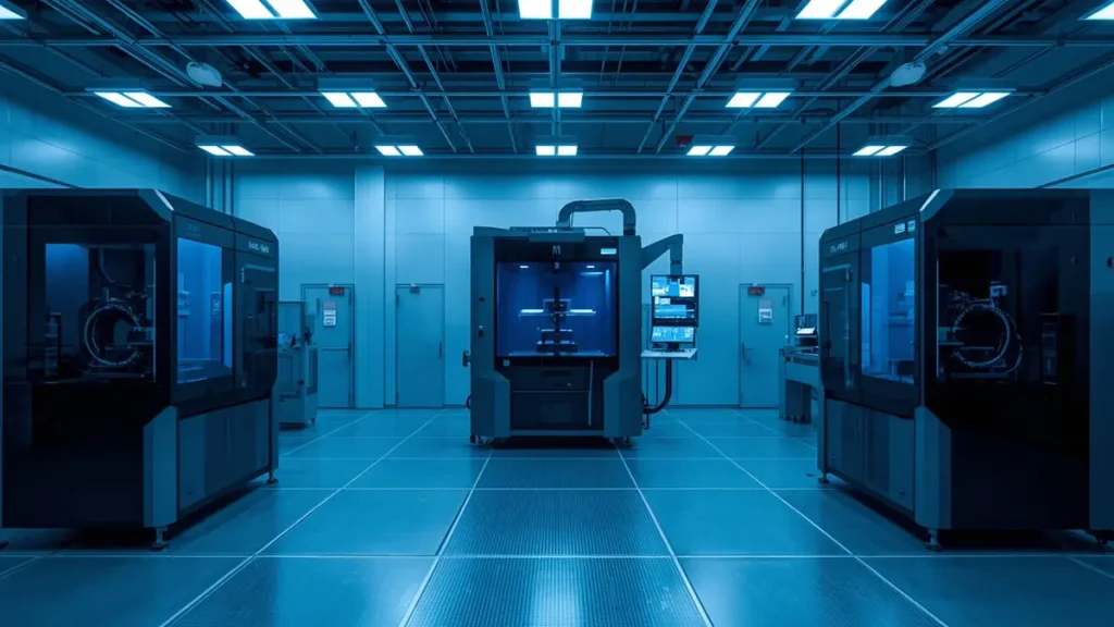
Advanced PCB Manufacturing Cleanroom & Automated Equipment
The routing density and reliability demands of modern industrial‑control boards are only achievable with process control that goes beyond basic multilayer fabrication. The following equipment runs on our Shenzhen production floor and is applied to industrial‑control builds, not reserved for flagship product lines only:
| Equipment | Function | Why it matters for a 6‑layer industrial‑control board |
|---|---|---|
| SCREEN Ledia LDI Exposure Machine | Laser Direct Imaging (precision pattern transfer) | Replaces film‑based phototools with direct laser exposure, giving consistent ultra‑fine line width/spacing and better layer‑to‑layer registration — supports the controlled‑impedance and BGA fan‑out routing common on PLC and motor‑control boards |
| Mitsubishi Electric UV/CO₂ Laser Drilling Machine | Blind/buried microvia drilling | Enables the laser‑microvia sizes (0.1–0.15 mm) used in HDI‑capable industrial‑control stackups, and supports mSAP‑processed fine‑line construction |
| Lauffer PCB Lamination System | High‑performance multilayer lamination | Precise temperature/pressure control reduces warpage and keeps dielectric thickness consistent — directly protects the impedance tolerance quoted on a six‑layer build |
| HX Automation PCB Plating Line | Automated electroplating | Delivers the consistent via‑copper and thick‑copper plating (up to 6 oz outer copper) needed for high‑current motor‑drive and power‑control paths |
| Hisun‑Test SIF‑2001 Automatic Impedance Test System (with Keysight VNA) | Impedance / insertion‑loss testing | Verifies as‑built ±5% (or tighter, on request) impedance for CAN, industrial Ethernet, and fieldbus interfaces before the board ships |
| Nordson DAGE XD7600NT X‑Ray Tester | Non‑destructive internal inspection | Confirms via alignment, BGA solder integrity, and internal structure — relevant to the resin‑plugged, 100%‑filled vias used in our industrial‑control construction |
Applying this equipment set to a six‑layer industrial‑control board is a matter of process discipline, not a marketing upgrade: registration accuracy, via integrity, and verified impedance are what determine whether the board performs correctly inside a control cabinet or on a factory floor. [Full equipment list and photos: pcbkr.com/advanced‑equipment‑ai‑server‑pcb]
Manufacturing Capabilities and Design Limits
The table below combines our published 6‑layer‑specific industrial‑control parameters with our general standard‑PCB fabrication limits.
| Capability | Published value | Source |
|---|---|---|
| Layer count (industrial‑control line) | 6–14 layers standard; up to 20 layers for high‑density control units | Intelligent Industrial Control PCB spec sheet |
| Base material | FR‑4 High‑Tg (Tg ≥ 180 °C) or halogen‑free FR‑4 (IT180A) | Intelligent Industrial Control PCB spec sheet |
| Board thickness | 1.6–3.2 mm, ±0.1 mm tolerance | Intelligent Industrial Control PCB spec sheet |
| Outer‑layer copper | 1–3 oz standard; up to 6 oz for power‑intensive circuits | Intelligent Industrial Control PCB spec sheet |
| Inner‑layer copper | 0.5–2 oz | Intelligent Industrial Control PCB spec sheet |
| Min trace/spacing, outer layers | 3–4 mil (75–100 μm) | Intelligent Industrial Control PCB spec sheet |
| Min trace/spacing, inner layers | 2.5–3 mil (62.5–75 μm) | Intelligent Industrial Control PCB spec sheet |
| Laser microvia size | 0.1–0.15 mm (4–6 mil) | Intelligent Industrial Control PCB spec sheet |
| Aspect ratio (PTH) | Up to 10:1 | Intelligent Industrial Control PCB spec sheet |
| Impedance control | ±5% for 50 Ω/90 Ω/100 Ω single‑ended and differential pairs | Intelligent Industrial Control PCB spec sheet |
| Surface finishes | ENIG (2–5 μ” Au), Hard Gold (15–30 μ” Au), high‑reliability OSP; HASL, Immersion Tin/Silver, ENEPIG also available | Intelligent Industrial Control PCB spec sheet / Standard PCB Capability |
| Solder mask | LPI green/black, 0.8–1.2 mil, ±0.05 mm registration to pads | Intelligent Industrial Control PCB spec sheet |
| Max board size, 4/6‑layer | 600×900 mm or 1200×450 mm (no design review required) | Standard PCB Capability |
| Max board size, >8‑layer | 600×700 mm or 1000×450 mm (high‑precision lamination) | Standard PCB Capability |
| Min board size | 0.4×0.8 mm (≤0.5 mm thick); 0.8×1.5 mm (>0.5 mm thick) | Standard PCB Capability |
| Mechanical routing tolerance | ±0.08 mm | Standard PCB Capability |
| Embedded passives | Resistors 10–100 kΩ, capacitors 10–100 nF, integrated into inner layers | Intelligent Industrial Control PCB spec sheet |
| Testing | AOI (Deep Learning‑based), impedance/TDR testing (Hisun‑Test SIF‑2001 + Keysight VNA), X‑ray inspection (Nordson DAGE XD7600NT), electrical test | Advanced Equipment / About Us |
| Quality standard | IPC‑6012 Class 3, IPC‑A‑600 Class 3, IPC‑4101A/B; ISO 9001:2015; UL 796 (File No. ZPMV2.E530232) | Intelligent Industrial Control PCB spec sheet / Certifications |
Note: figures above are published on pcbkr.com as of this writing. Please confirm current values with our engineering team at the time of quotation, as process capability is periodically upgraded.
Industrial‑Control Reliability Requirements
IPC Class 2 or Class 3?
IPC Class 2 may be appropriate for general industrial equipment where standard field service is available. Our published industrial‑control line is built and tested to IPC‑6012 Class 3 and IPC‑A‑600 Class 3 as a baseline — appropriate where uninterrupted operation, safety functions, harsh environments, or difficult service access raise the cost of a field failure. The correct class for your specific product should still be confirmed against your end‑product standard and risk assessment.
Thermal cycling and temperature exposure
Our industrial‑control boards are rated for an operating temperature range of ‑40 °C to +85 °C standard, extending to ‑55 °C to +125 °C in the high‑grade configuration, and are qualified to 1,000+ thermal shock cycles (‑40 °C ↔ +125 °C) with no delamination, using High‑Tg FR‑4 (Tg ≥ 180 °C) to control Z‑axis expansion and delamination risk.
Insulation resistance and moisture reliability
Published performance includes insulation resistance ≥ 1×10¹² Ω at 500 V DC, dielectric withstanding voltage ≥ 1500 V AC for 1 minute, and humidity resistance of 85% RH at 85 °C for 1,000+ hours with no corrosion (IPC‑A‑600 Class 3 acceptance). These figures are relevant when evaluating CAF risk and long‑term insulation performance on boards operating at higher working voltages or in humid industrial environments.
Creepage, clearance, and isolation
Required spacing still depends on your working voltage, insulation category, pollution degree, and the safety standard applicable to your finished equipment. Our engineering team reviews these values against your governing standard (e.g., UL/IEC industrial safety standards referenced in our UL 796 recognition) rather than applying a single universal number.
Vibration, shock, and mechanical reliability
Board thickness (1.6–3.2 mm), copper distribution, and mounting‑hole layout are reviewed together with your connector and component loading to suit factory‑floor vibration, vehicle‑mounted equipment, or other mechanical‑cycling environments.
Testing and Inspection
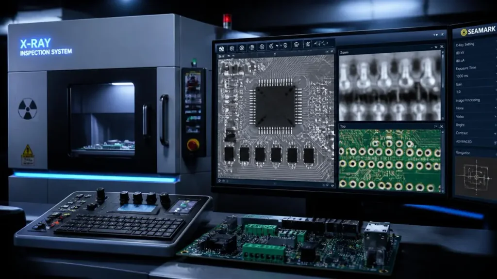
X-Ray Quality Control and Solder Inspection for Industrial Control PCBs
| Test or inspection | What it verifies | Equipment / standard used |
|---|---|---|
| DFM review | Manufacturability before production | In‑house engineering review |
| AOI | Etch‑ and assembly‑related visual defects | Deep Learning‑based AOI (and AVI) |
| Impedance / TDR testing | As‑built controlled impedance | Hisun‑Test SIF‑2001 Automatic Impedance Test System with Keysight VNA |
| X‑ray inspection | Via alignment, BGA solder quality, internal structure | Nordson DAGE XD7600NT X‑Ray Tester |
| Electrical test | Continuity and isolation | Flying‑probe / fixture test (confirm scope per order) |
| Thermal stress testing | Reliability under temperature exposure | 1,000+ cycle thermal shock qualification (IPC‑6012 Class 3) |
| Dimensional inspection | Thickness, profile, holes, registration | ±0.08 mm mechanical routing tolerance |
What is included in your quality package?
Buyers should confirm, before ordering: which of the above are included in a standard quotation versus billed separately; whether impedance/test coupons are built into the production panel; whether inspection applies to every board or to sample boards; and how nonconforming material is handled. Our quality system operates under ISO 9001:2015 (Certificate No. 68626Q00015R000) with full material and process traceability aligned to IPC‑2581 Revision C for our industrial‑control line — ask your account contact for the specific test report package for your order.
Prototype, Pilot, and Mass Production
Prototype stage
Gerber and drill‑file review, stackup proposal, DFM feedback, and first‑article documentation. We publish a 72‑hour fast‑sample delivery track for high‑precision PCB and a No MOQ policy for new product introduction, supported by our LDI/laser‑drilling/lamination equipment line rather than a separate low‑volume process.
Pilot production
Process repeatability checks, assembly‑yield review, test‑fixture validation, and first‑article approval using the same equipment and stackup that will run in volume — not a separate “prototype‑only” process.
Volume production
Material reservation, panelization, lot traceability (per IPC‑2581 Revision C), ongoing electrical/impedance testing, and change‑control notifications, run on our automated plating line and AOI/X‑ray inspection stations.
Repeat‑order support
‑ Can we reproduce the exact same stackup on the next order? — Yes, the approved stackup and material system are recorded against the part number under our ISO 9001:2015 quality system. ‑ Are design revisions locked? — Traceability is maintained per IPC‑2581 Revision C to prevent an outdated file from re‑entering production. ‑ Is customer design data protected? — [Confirm current NDA/file‑retention policy with your account manager for publication here.]
Six‑Layer PCB Cost and Lead Time
We do not publish a single universal price for a six‑layer PCB, because board size, quantity, materials, copper weight, testing, and tolerances change the cost significantly from one order to the next. Send your Gerber/ODB++ files and specifications to sales@pcbkr.com for a configuration‑specific quotation.
What affects the quotation
Board dimensions (up to 600×900 mm / 1200×450 mm for a 6‑layer board without design review); quantity; finished thickness (1.6–3.2 mm); copper weights (up to 6 oz outer); material grade (standard FR‑4 vs. High‑Tg vs. low‑loss); trace/spacing (down to 3–4 mil outer, 2.5–3 mil inner); laser‑microvia use; surface finish; controlled‑impedance requirements (±5% standard); testing scope; and delivery location.
How buyers should compare quotations
Confirm both quotes cover: the same board revision; the same material family (standard FR‑4 vs. High‑Tg IT180A‑class); the same finished copper; the same surface finish (e.g., ENIG vs. OSP); the same impedance requirement and tolerance; the same testing scope (AOI, impedance/TDR, X‑ray); the same acceptance class (IPC Class 2 vs. Class 3); and the same tooling/engineering charges.
Lead‑time explanation
Total delivery time runs through engineering review, material preparation, inner‑layer imaging (SCREEN Ledia LDI), lamination (Lauffer system), laser drilling and plating (Mitsubishi laser drill, HX Automation plating line), surface finish, impedance/X‑ray testing, and final inspection. We publish a 72‑hour fast‑sample track for high‑precision prototype builds; production lead time for six‑layer industrial‑control boards should be confirmed at quotation based on your specific stackup, material, and testing requirements.
How to Select a Six‑Layer Industrial PCB Manufacturer
Technical capability
Can the supplier manufacture the required stackup and hold ±5% impedance tolerance? Does it support 3–4 mil trace/space and 0.1–0.15 mm laser microvias? Can its engineers review industrial‑control isolation and thermal issues, not just fabricate what is submitted?
Quality system
PCBKR holds ISO 9001:2015 (No. 68626Q00015R000, valid through August 1, 2029), UL recognition under File No. ZPMV2.E530232 (UL 796, covering multilayer HD‑1 and single‑layer HD‑2 boards), and RoHS 2.0 compliance (Test Report No. HS202601082028‑1ER). ISO 14001:2015, IATF 16949:2016, and ISO 13485:2016 are additionally referenced on our site — verify current scope and validity with our team for your specific application (automotive, medical, etc.).
Engineering communication
Our DFM review is provided ahead of production release, with a documented stackup‑approval step so you see exactly what will be built before panels are cut.
Delivery and supply continuity
Material sourced from an approved supplier list (SY, ITEQ, KB, NanYa, Doosan, Isola, TUC, EMC, Ventec); No MOQ policy; 72‑hour fast‑sample track; full material/process traceability per IPC‑2581 Revision C.
Commercial transparency
Request a complete quotation covering tooling and testing charges, Incoterms, payment terms, sample policy, and warranty/replacement terms alongside the unit price.
[Request a 6‑Layer Industrial‑Control PCB Quote →] Email:pcb@pcbkr.com
Frequently Asked Questions
What is a six‑layer PCB?
A six‑layer PCB contains six conductive copper layers separated by dielectric material and bonded into one multilayer board. The additional layers provide more routing capacity, reference planes, power‑distribution options, and electromagnetic compatibility control than a basic two‑ or four‑layer board.
What are six‑layer PCBs used for in industrial control?
PLCs, motor drives and VFDs, industrial power supplies, EtherCAT/PROFINET gateways, IIoT edge controllers, process instrumentation, and solar/wind power‑conversion equipment — the application scope PCBKR’s industrial‑control line is built around.
Why use a six‑layer PCB instead of a four‑layer PCB?
A six‑layer board provides additional routing space, more stable reference planes, improved separation between noisy and sensitive circuits, and support for ±5% controlled impedance — useful once signal count, edge rate, or EMC risk outgrow a four‑layer stackup.
What is the best six‑layer PCB stackup?
There is no universal best stackup. A common industrial arrangement places signal layers next to solid ground references and assigns internal layers to signals or power; the final choice depends on impedance targets, copper weights, thickness, and thermal needs, confirmed with our engineering team before production.
What materials are used for industrial six‑layer PCBs?
PCBKR’s industrial‑control line standardizes on FR‑4 High‑Tg (Tg ≥ 180 °C), including the halogen‑free IT180A‑class material, with M7/M8/M9‑grade low‑loss laminates available for higher‑speed interfaces.
Are six‑layer PCBs suitable for PLC control boards?
Yes — our published spec sheet lists factory automation and PLC control units, including EtherCAT/PROFINET communication, as a core application for the 6–14‑layer industrial‑control line.
How does a six‑layer PCB help reduce EMI?
A suitable stackup places signals close to continuous reference planes and shortens return‑current paths. Layer count alone does not guarantee EMC performance — grounding, routing, filtering, and enclosure design also matter.
Can a six‑layer PCB support controlled impedance?
Yes. PCBKR holds ±5% impedance tolerance for 50 Ω/90 Ω/100 Ω single‑ended and differential structures on its industrial‑control line, verified using a Hisun‑Test SIF‑2001 system with Keysight VNA.
Do industrial‑control PCBs need IPC Class 3?
Not automatically for every product, but PCBKR’s published industrial‑control line is built and tested to IPC‑6012 Class 3 / IPC‑A‑600 Class 3 as a baseline; confirm the correct class for your end product with your quality agreement.
What causes delamination in a multilayer PCB, and how is it controlled?
Delamination risk rises with thermal stress, unsuitable materials, and moisture. PCBKR’s industrial‑control boards use High‑Tg FR‑4 and are qualified to 1,000+ thermal shock cycles (‑40 °C to +125 °C) with no delamination.
How much does a six‑layer PCB cost?
There is no reliable universal price — cost depends on dimensions, quantity, material, copper weight, via structure, surface finish, impedance, and testing. Send Gerber/ODB++ files and specifications to sales@pcbkr.com for a configuration‑specific quote.
What files are required for a six‑layer PCB quotation?
Gerber or ODB++ data, drill files, board outline, stackup requirements, fabrication drawing, quantity, material, thickness, copper weights, surface finish, impedance requirements, and inspection/acceptance requirements.
Do you support low‑volume and high‑volume production?
Yes — PCBKR publishes a No MOQ policy for new product introduction alongside mass‑production capability; confirm current minimum quantities and panel capacity with your account contact for your specific board.
What certifications does Shenzhen Hongda Circuit Technology hold?
ISO 9001:2015 (Certificate No. 68626Q00015R000, valid through August 1, 2029), UL recognition (File No. ZPMV2.E530232, UL 796), and RoHS 2.0 compliance (Test Report No. HS202601082028‑1ER), alongside ISO 14001:2015, IATF 16949:2016, and ISO 13485:2016 referenced on our certifications page.
Request Your 6‑Layer Industrial‑Control PCB Quote
‑ Request a 6‑Layer Industrial‑Control PCB Quote ‑ Upload Gerber Files for DFM Review ‑ Request a Recommended Stackup ‑ Download the 6‑Layer PCB Capability Sheet ‑ Ask an Engineer About Impedance or Reliability ‑ Request a Prototype‑to‑Production Plan
RFQ form fields: Name · Business email · Company · Country/region · Board quantity · Prototype or production requirement · Board size · Layer count · Material/Tg · Finished thickness · Copper weight · Surface finish · Controlled‑impedance requirement · Target delivery date · File upload · Additional application details.
After you submit, you will receive: a preliminary manufacturability review, a stackup recommendation referencing our 6–14‑layer industrial‑control build, clarification of any missing specifications, the main cost drivers for your design, an estimated production schedule, testing recommendations (AOI / impedance‑TDR / X‑ray), and a named technical contact at sales@pcbkr.com.
Shenzhen Hongda Circuit Technology Co., Ltd. (PCBKR) — www.pcbkr.com — sales@pcbkr.com — +86 0755 23720053
About Author
David Chen https://www.linkedin.com/in/pcbcoming
David Chen boasts an extensive professional background in PCBA manufacturing, PCBA testing, and PCBA optimization, with specialized expertise in high-precision PCBA fault analysis and rigorous PCBA reliability testing. The author has worked with high-layer-count server PCB fabrication, ultra-low-loss backplane stackups, and thermo-mechanical reliability optimization for AI infrastructure projects involving 112G and 224G PAM4 architectures. Skilled in complex circuit design and cutting-edge advanced PCB manufacturing processes, he delivers solutions that elevate product durability and performance across industrial applications. His technical articles focusing on PCBA manufacturing workflows and testing methodologies are widely cited by industry peers, research institutions, and technical platforms, solidifying his reputation as a recognized technical authority in the global circuit board manufacturing sector.