The Ultimate Procurement Guide to Impedance Controlled PCBs: From Stackup Engineering to Supplier Qualification for 224G PAM4 and AI Server Applications
An impedance controlled PCB is a precision-engineered circuit board where trace geometry, dielectric materials, and manufacturing tolerances are tightly regulated to maintain consistent electrical impedance—typically 50Ω single-ended or 90Ω/100Ω differential—across high-speed signal paths. For procurement teams sourcing boards for 5G infrastructure, AI accelerators, or automotive radar, selecting the right controlled impedance PCB manufacturer determines whether your hardware achieves first-pass signal integrity or fails in the field.
1. Why Impedance Control Is Non-Negotiable in Modern PCB Procurement
1.1 The Procurement Risk: When Signal Integrity Becomes a Supply Chain Problem
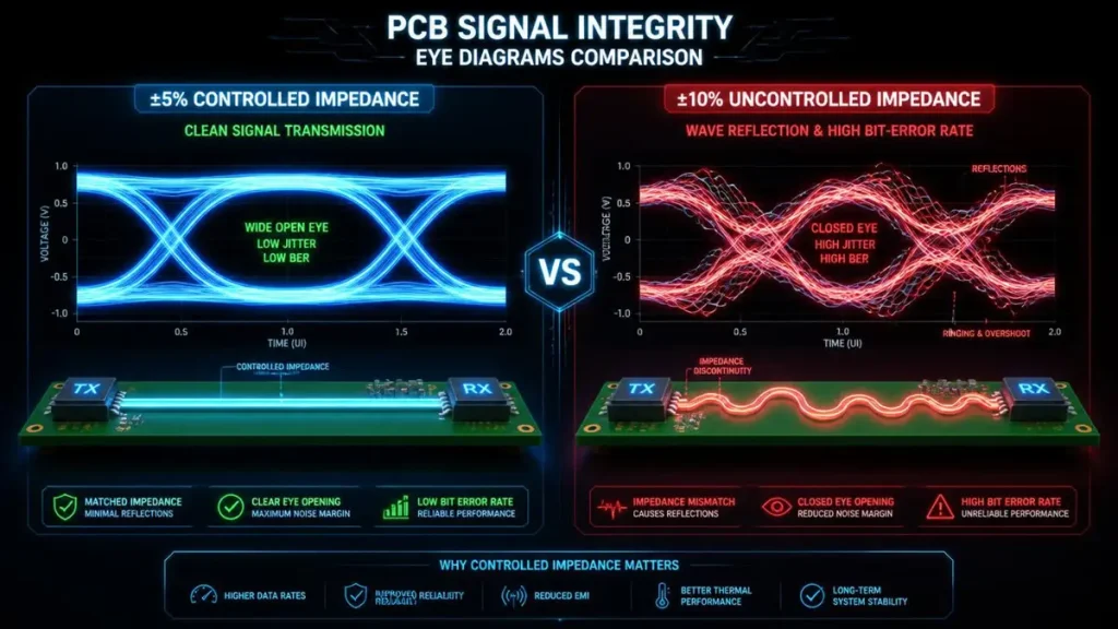
PCB Signal Integrity Comparison: ±5% Controlled Impedance vs Uncontrolled Impedance
If you are evaluating PCB suppliers for data-center switches, GPU backplanes, or automotive ADAS modules, impedance control is no longer a secondary specification—it is a procurement-critical parameter. When trace lengths exceed one-tenth of the signal rise-time wavelength, transmission-line effects dominate. Any deviation from target impedance creates reflections, eye-diagram closure, and bit-error-rate (BER) failures that no post-assembly debugging can fix.
In 2026, the threshold for mandatory controlled impedance has dropped dramatically. A PCIe Gen 5 interface at 32 GT/s, a 112G PAM4 SerDes lane, or a 224G backplane trace demands differential impedance tolerances of ±5% or tighter, with some AI server designs pushing for ±3% on critical nets. For procurement teams sourcing boards for 5G infrastructure, AI accelerators, or automotive radar, selecting the right controlled impedance PCB manufacturer determines whether your hardware achieves first-pass signal integrity or fails in the field. For a detailed technical dive into dielectric constants, stackups, and field solver calculations, explore our guide on What Is Impedance Control in PCB? A Complete Procurement & Engineering Guide.
1.2 When Your BOM Demands Controlled Impedance PCB Specification
Not every board needs impedance control, but the following application categories make it mandatory in your RFQ:
| Application Tier | Typical Speed | Impedance Requirement | Tolerance |
|---|---|---|---|
| Consumer IoT / Industrial | < 1 Gbps | 50Ω SE, 100Ω Diff | ±10% |
| Automotive Ethernet / 5G Sub-6 | 1–10 Gbps | 100Ω Diff | ±8% |
| AI Server / 112G PAM4 | 25–56 Gbps | 85–100Ω Diff | ±5% |
| 224G PAM4 Backplane / HPC | 112–224 Gbps | 92–100Ω Diff | ±3%–±5% |
Procurement insight: If your design includes DDR5 memory interfaces, multi-gigabit Ethernet, or any PAM4 signaling, your fabrication drawing must explicitly call out controlled impedance PCB manufacturing notes with target values, trace geometries, and test methods. Omitting this detail shifts liability to your engineering team when boards arrive untested for impedance.
2. How to Evaluate Impedance Controlled PCB Manufacturers: A Procurement Scoring Matrix
2.1 Technical Capability Verification: Beyond the Marketing Brochure
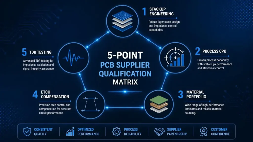
5-Point PCB Supplier Qualification Matrix for Controlled Impedance Manufacturing
When qualifying a controlled impedance PCB supplier, request evidence across five technical dimensions:
- Stackup Engineering Depth A qualified manufacturer should not ask you to “provide the stackup.” Instead, they should propose a manufacturer-validated stackup using characterized Dk/Df values from their actual material inventory—not catalog assumptions. At Shenzhen Hongda Circuit Technology Co., Ltd., our engineering team analyzes dielectric material selection at operating frequency, layer assignment for microstrip versus stripline routing, and via stub mitigation before you commit to layout. This pre-layout collaboration eliminates the costly respin cycle that occurs when a designer completes routing only to discover the stackup is unmanufacturable.
- Impedance Tolerance and Process Capability (Cpk) Standard industry tolerance is ±10%. For high-speed designs, you need ±5% impedance tolerance as standard, with ±3% available on request. Critically, ask for Cpk statistics. A Cpk ≥ 1.33 indicates the process is statistically capable of holding tolerance. Our 2026 manufacturing data shows consistent Cpk values above 1.33 on controlled impedance layers, validated through 100% TDR testing on every production panel.
- Material Portfolio and Frequency Characterization The supplier must offer more than “FR-4.” For 112G/224G PAM4 designs, verify access to:
- Ultra-low-loss laminates: Megtron 6/7, Rogers 4350B/5880, Isola FR408HR, Taconic RF-35
- Low-profile copper foils: VLP (Very Low Profile) and HVLP (Hyper Very Low Profile) to mitigate skin-effect losses at 56 GHz
- Flat glass styles (e.g., 1078, 1035) to reduce fiber weave effect-induced impedance variation
- Etching Compensation and Trapezoidal Trace Control Chemical etching is isotropic. The final trace width is narrower than the artwork, and the cross-section becomes trapezoidal—not rectangular. A mature manufacturer applies etch compensation per copper weight and layer type, with real-time SPC monitoring. Ask to see their etch-compensation table and whether they model trapezoidal geometry in their impedance pre-calculations.
- TDR Testing Infrastructure and Coupon Design Every panel must include impedance test coupons representative of production traces. The supplier should test 50Ω single-ended, 85Ω/100Ω differential structures, and provide formal impedance test reports with measured vs. target values and Cpk statistics. At PCBkr, we archive TDR results for full traceability and include them in the delivery documentation package.
2.2 Certification and Quality System Audit Checklist
| Certification | What It Proves | Red Flag |
|---|---|---|
| ISO 9001:2015 | Systematic quality management | Certificate expired or scope excludes PCB fabrication |
| IPC-6012 Class 3 / 3A | High-reliability acceptance criteria | Supplier only offers Class 2 for “cost savings” on high-speed designs |
| IATF 16949 | Automotive-grade process control | Missing if you supply Tier-1 automotive OEMs |
| ISO 13485 | Medical device traceability | Critical for implantable or diagnostic hardware |
| AS9100D | Aerospace quality baseline | Required for defense and avionics procurement |
| UL / ITAR | Safety and export compliance | Absence blocks North American defense contracts |
2.3 Equipment and Process Technology: The 2026 Capability Benchmark
Modern impedance controlled PCB manufacturing requires specific equipment investments. During your factory audit or virtual capability review, verify the following:
- LDI (Laser Direct Imaging): SCREEN Ledia or equivalent for ±25μm interlayer alignment, critical for 3-mil trace/space impedance layers
- Laser Drilling: Mitsubishi or similar for 0.1 mm microvias with ±25μm positional accuracy
- 3D X-Ray (AXI): Nordson DAGE or equivalent for 100% inspection of blind/buried via integrity
- TDR Oscilloscope: Keysight or Tektronix with < 35 ps rise time for accurate impedance profiling
- mSAP (modified Semi-Additive Process): Enables 20 μm line/space for ultra-fine impedance control on HDI layers
At Shenzhen Hongda Circuit Technology, our 2026 equipment lineup includes all of the above. Our full production upgrade integrates AI-driven process control that monitors etch line parameters in real time, detecting drift before panels are affected.
3. Material Selection for High-Speed Impedance Control: A Procurement Decision Framework
3.1 Dielectric Constant (Dk) and Dissipation Factor (Df): The Physics Behind the Purchase
Impedance is not a static number. Dk varies with frequency and temperature; Df determines how much signal energy converts to heat. For procurement teams, this means the material specified in the datasheet at 1 GHz may behave differently at 28 GHz.
2026 Material Selection Guide for Impedance Controlled PCBs
| Material | Dk @ 10 GHz | Df @ 10 GHz | Best For | Cost Index |
|---|---|---|---|---|
| Standard FR-4 | 4.2–4.5 | 0.020–0.025 | < 5 Gbps, cost-sensitive | 1.0× |
| High-Tg FR-4 | 4.2–4.4 | 0.018–0.022 | Automotive, industrial | 1.2× |
| Isola FR408HR | 3.68 | 0.0092 | 10–25 Gbps, mid-range | 1.8× |
| Panasonic Megtron 6 | 3.17 | 0.002 | 56–112 Gbps, AI servers | 3.5× |
| Rogers 4350B | 3.48 | 0.0037 | RF/microwave, 5G mmWave | 4.0× |
| Rogers 5880 | 2.20 | 0.0009 | 77 GHz radar, aerospace | 6.0× |
Procurement tip: Do not accept “equivalent material” substitutions without documented Dk/Df characterization at your operating frequency. A supplier offering Megtron 6 at a 20% discount may be using unverified parallel imports with batch-to-batch Dk variation that destroys impedance consistency.
3.2 Fiber Weave Effect and Copper Roughness: Hidden Yield Killers
Two often-overlooked material issues directly impact impedance yield:
Fiber Weave Effect: Standard 1080 or 2116 glass cloth creates localized Dk variation as traces align with glass bundles versus resin-rich areas. This causes impedance discontinuities on long differential pairs. Mitigation strategies include:
- Specifying flat-glass styles (1078, 1035, 1067) with more uniform resin distribution
- Implementing zig-zag routing angles (10°–15° offset) to average out weave periodicity
- Requiring the manufacturer to model weave effect in pre-production simulation
Copper Foil Roughness: At 224G PAM4 frequencies, skin depth shrinks to sub-micron levels. Standard STD copper with 6–8 μm Rz roughness increases conductor loss by 30–50% compared to HVLP copper with <2 μm Rz. Your fabrication notes should explicitly specify VLP or HVLP copper for all high-speed layers.
3.3 Rigid-Flex and Hybrid Stackup Procurement Considerations
For aerospace, medical, or compact 5G wearable designs, rigid-flex impedance controlled PCBs introduce additional procurement variables:
- Adhesiveless copper on flex layers avoids impedance shift from acrylic adhesive Dk variation
- Low-Dk coverlay materials (e.g., Panasonic Felios) replace standard polyimide coverlay on critical flex traces
- Separate impedance calculations are required for rigid and flex sections—never assume a single stackup applies across both
4. Stackup Design and Trace Geometry: The Engineering-Procurement Interface
4.1 Microstrip vs. Stripline: Cost and Performance Trade-offs
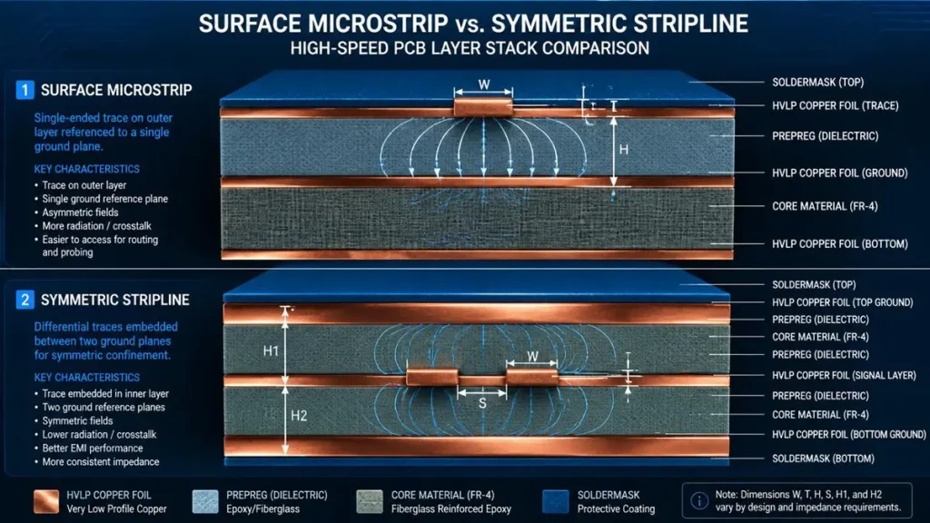
Surface Microstrip vs Symmetric Stripline High-Speed PCB Layer Stack Comparison
| Topology | Structure | Impedance Stability | EMI | Relative Cost |
|---|---|---|---|---|
| Surface Microstrip | Trace on outer layer, one reference plane | Moderate (solder mask Dk affects value) | Higher | Lower |
| Embedded Microstrip | Trace buried in prepreg, one reference | Good | Moderate | Medium |
| Symmetric Stripline | Trace between two reference planes | Excellent | Lowest | Higher (more layers) |
| Asymmetric Stripline | Trace closer to one reference | Good | Low | Medium |
Procurement recommendation: For 112G PAM4 and above, mandate stripline routing for all critical differential pairs. The additional lamination cycle increases board cost by 40–60% versus microstrip, but the EMI containment and impedance stability are non-negotiable at these data rates.
4.2 Real-World Calculation Example: From Polar Si9000 to Purchase Order
Understanding the supplier’s calculation methodology helps you validate quotations and spot unrealistic claims.
Example: 100Ω Differential Stripline for PCIe Gen 6
- Target: 100Ω ±5% (95Ω–105Ω)
- Material: Megtron 6, Dk = 3.17 @ 16 GHz
- Core thickness (H): 4 mil
- Copper weight: 1 oz (1.2 mil finished after plating)
- Using Polar Si9000 or Saturn PCB Toolkit, the solver outputs:
- Trace width: 3.2 mil
- Pair spacing: 4.8 mil
- Expected tolerance band: 3.0–3.4 mil width to hold impedance within ±5%
If a supplier quotes this stackup with 3-mil trace/space capability but cannot show etch-compensation data for 1-oz copper on Megtron 6, the quoted tolerance is theoretical. At PCBkr, we validate every stackup with in-house simulation and provide pre-production impedance modeling reports as part of our complimentary DFM review.
4.3 Differential Pair Matching and EDA Tool Integration
Ensure your supplier’s engineering team can read and validate impedance constraints from your native EDA format (Altium Designer, Cadence Allegro, Mentor Xpedition). Key DRC rules to verify during DFM review:
- Length matching within ±5 mils for DDR5 byte lanes
- Phase matching (intra-pair skew) < 1 ps for 112G PAM4
- Neck-down rules at via transitions and connector launches
- Void avoidance in reference planes under differential pairs
5. Manufacturing Tolerances, DFM, and Testing: What Procurement Must Specify
5.1 Fabrication Variables That Cause Impedance Drift
Even with perfect design, manufacturing introduces physical variation. Your fabrication drawing must account for:
| Variable | Typical Impact | Specification to Include |
|---|---|---|
| Etch undercut | Trace width reduction 0.3–0.8 mil per side | Etch compensation applied; trapezoidal shape modeled |
| Lamination thickness | ±10% on standard, ±5% on tight-tolerance | Specify prepreg sheet count, not just finished thickness |
| Copper plating distribution | Thickness variation 20–30% across panel | Specify minimum and average copper weight |
| Solder mask thickness | 0.5–1.5 mil; Dk ≈ 3.3–4.0 | Include mask in impedance calculation for microstrips |
| Drill positional accuracy | ±50 μm mechanical, ±25 μm laser | Critical for microvia-based HDI impedance layers |
5.2 How to Write Controlled Impedance Fabrication Notes
Vague notes like “control impedance per IPC-2221” create ambiguity. Use this template in your fabrication drawing:
plaintext
CONTROLLED IMPEDANCE REQUIREMENTS:
1. Single-ended impedance: 50Ω ±5% (47.5Ω–52.5Ω)
2. Differential impedance: 100Ω ±5% (95Ω–105Ω)
3. Test method: TDR per IPC-TM-650 2.5.5.7
4. Test coupon: Include on every panel; 50Ω SE, 100Ω Diff, 85Ω Diff (if applicable)
5. Report: Provide TDR waveform and measured impedance table per panel
6. Material: Megtron 6 or approved equivalent; Dk characterized at 16 GHz
7. Copper foil: HVLP on all signal layers
8. Tolerance validation: Cpk ≥ 1.33 required
5.3 TDR Testing and Coupon Design: The Verification Standard
Impedance verification uses Time Domain Reflectometry (TDR), injecting a fast-rise-time pulse and measuring reflected voltage. Deviations appear as reflections, enabling precise trace impedance measurement. Industry best practice requires impedance test coupons on each panel, in locations representative of production traces.
At Shenzhen Hongda Circuit Technology, every controlled impedance panel undergoes 100% TDR testing. Our standard coupon design includes 50Ω single-ended microstrip/stripline, 100Ω and 85Ω differential structures, and length-matched coupons for measurement repeatability. Test results—including measured vs. target impedance and Cpk statistics—are archived and provided as part of the delivery documentation.
5.4 Cost Trade-offs: ±5% vs. ±10% and the Total Cost of Ownership
Tightening impedance tolerance from ±10% to ±5% increases manufacturing complexity but often reduces total system cost:
| Tolerance | Direct PCB Cost Impact | System-Level Risk | TCO Recommendation |
|---|---|---|---|
| ±10% | Baseline | Higher BER, potential respins | Acceptable for < 5 Gbps |
| ±5% | +15–25% | Controlled SI, stable yield | Required for 10–56 Gbps |
| ±3% | +40–60% | Minimal margin, high yield | Justified for 112G+ PAM4 |
Procurement strategy: For prototype runs, specify ±5% to validate design margins. For volume production of 112G+ designs, negotiate ±3% on critical nets with ±5% on secondary interfaces. This hybrid approach optimizes cost without compromising signal integrity.
6. Sourcing Strategy: From Prototype to Volume Production
6.1 The Procurement Decision Chain for Impedance Controlled PCBs
A disciplined sourcing process for controlled impedance PCB manufacturing follows five stages:
- Stage 1: Requirement Definition Document all impedance targets, layer count, material requirements, and test protocols before issuing RFQ. Include stackup preliminary, connector datasheets, and impedance table.
- Stage 2: Supplier Shortlist Qualify 2–3 suppliers against the scoring matrix in Section 2.1. Request stackup proposals, not just unit prices.
- Stage 3: DFM and Stackup Validation Engage the supplier’s engineering team for pre-layout stackup review. A 3–5 day investment here prevents 2–4 week respins later.
- Stage 4: First Article Qualification (FAQ) Order 5–10 pieces. Verify TDR reports, microsection data, and impedance Cpk. Do not skip this step for high-speed designs.
- Stage 5: Volume Negotiation Lock material allocation, tolerance bands, and test documentation requirements in the production agreement. Negotiate price based on panel utilization and lead time, not just per-piece cost.
6.2 Why Shenzhen Hongda Circuit Technology (PCBkr) for Your Impedance Controlled PCB Program
Shenzhen Hongda Circuit Technology Co., Ltd. operates as a dual-capability manufacturing partner: we deliver the elite technical ceiling required for next-gen AI hardware (224G backplanes, 40-layer HPC substrates, mSAP fine-line processing) while maintaining the flexibility, rapid turnaround, and cost-efficiency needed for mid-to-high-volume production.
2026 Capability Highlights:
- Layer count: 2 to 40+ layers, including 104-layer backplanes
- Impedance control: ±5% standard, ±3% available; Cpk ≥ 1.33
- Minimum trace/space: 3 mil / 3 mil standard; 20 μm / 20 μm with mSAP
- Materials: Standard FR-4 through Megtron 6/7, Rogers 4350B/5880, Isola, Taconic
- Testing: 100% TDR on all controlled impedance panels; 100% 3D X-Ray (AXI)
- Certifications: ISO 9001, IATF 16949, ISO 13485, AS9100D, IPC-6012 Class 3/3A, UL, ITAR
- Alignment: ±25 μm interlayer registration (down from ±75 μm industry typical)
Our Commitment: Submit your Gerber files, stackup requirements, and impedance targets to sales@pcbkr.com. Our engineering team returns a complimentary DFM review, manufacturer-validated stackup proposal, and detailed quotation within 30 minutes for standard inquiries and 24 hours for complex 224G/AI server projects.
7. FAQ: Impedance Controlled PCB Procurement — Answers for Buyers and Sourcing Managers
What is an impedance controlled PCB, and why is it necessary for my project?
An impedance controlled PCB is a circuit board manufactured with tightly regulated trace geometry and dielectric properties to maintain consistent electrical impedance—typically 50Ω for single-ended signals and 90Ω or 100Ω for differential pairs. It is necessary whenever your design operates above approximately 100 MHz or includes high-speed digital interfaces like PCIe, DDR, Ethernet, or PAM4 SerDes. Without impedance control, signal reflections cause data errors, EMI compliance failures, and intermittent system crashes that are impossible to debug after assembly.
What materials should I specify for 112G PAM4 or AI server backplane PCBs?
For 112G PAM4 and 224G backplane designs, specify ultra-low-loss laminates with stable Dk/Df through 56 GHz. Our recommended hierarchy: Megtron 6 or 7 for mainstream AI server motherboards; Rogers 4350B for RF-hybrid designs; and Rogers 5880 for 77 GHz automotive radar or aerospace applications. Always pair these with HVLP copper foil and flat-glass prepreg styles (1078/1035) to minimize fiber weave effect and conductor loss.
When should I specify controlled impedance in my fabrication drawing, and what information must I include?
Specify controlled impedance before you release your design for quotation. Your fabrication notes must include: target impedance values (e.g., 50Ω, 100Ω), tolerance band (e.g., ±5%), test method (TDR per IPC-TM-650), required test coupon structures, material grade with frequency-specific Dk, copper foil type, and minimum Cpk requirement. Vague notes like “control impedance per IPC” expose you to supplier interpretation and potential respins.
How do manufacturing tolerances affect my total cost of ownership, and what tolerance should I negotiate?
Standard ±10% impedance tolerance is cheapest upfront but carries hidden system-level risk: higher BER, field failures, and redesign costs. ±5% adds 15–25% to direct PCB cost but dramatically improves yield and signal integrity margins for 10–56 Gbps designs. ±3% is premium-priced (+40–60%) but justified for 112G/224G PAM4 where every decibel of insertion loss budget matters. Our recommendation: prototype at ±5% to validate margins, then negotiate a hybrid specification (±3% on critical nets, ±5% on secondary) for volume production to optimize total cost of ownership.
Company Contact Info
Company: Shenzhen Hongda Circuit Technology Co., Ltd. (PCBkr)
Website: www.pcbkr.com
Email: sales@pcbkr.com
Phone: +86 0755 23720053
Address: Room 1608-1610, Research Development Comprehensive Building, Baoyunda Logistics Center, Baoan, Shenzhen, China
Unified Social Credit Code: 91440300MA5F6CA091
Certifications: ISO 9001:2015 | AS9100D | IPC-6012 Class 3/3A | ISO 13485 | IATF 16949 | UL | ITAR
About Author
David Chen https://www.linkedin.com/in/pcbcoming
David Chen boasts an extensive professional background in PCBA manufacturing, PCBA testing, and PCBA optimization, with specialized expertise in high-precision PCBA fault analysis and rigorous PCBA reliability testing. The author has worked with high-layer-count server PCB fabrication, ultra-low-loss backplane stackups, and thermo-mechanical reliability optimization for AI infrastructure projects involving 112G and 224G PAM4 architectures. Skilled in complex circuit design and cutting-edge advanced PCB manufacturing processes, he delivers solutions that elevate product durability and performance across industrial applications. His technical articles focusing on PCBA manufacturing workflows and testing methodologies are widely cited by industry peers, research institutions, and technical platforms, solidifying his reputation as a recognized technical authority in the global circuit board manufacturing sector.