Copper Base PCB Price Guide: Cost Factors and Quotation Tips
Copper Base PCB Price is the top urgent question on every sourcing manager’s mind when they key in “copper base PCB manufacturer” on Google at 11 p.m. amid an impending project deadline—and they are almost never searching for polished marketing brochures. What they truly need to clarify is why their received copper base PCB quotation is triple the cost of an aluminum MCPCB, whether the pricing is reasonable and market-aligned, and which supplier can reliably produce circuit boards that strictly match all drawing specifications.
Compiled by the engineering team at Shenzhen Hongda Circuit Technology Co., Ltd., this guide breaks down the complete cost calculation logic, reviews the full 2026 copper base PCB manufacturing technology landscape, and outlines actionable practical verification checkpoints to help buyers distinguish a justifiable copper base PCB quote from misleading low-cost traps.
What Is a Copper Base PCB and Why Does the Pricing Logic Differ From Ordinary Metal-Core Boards?
Metal-core PCB, or MCPCB, is often treated as a single product category, but aluminum
based and copper-based constructions sit at opposite ends of the cost and performance
spectrum. Aluminum MCPCB is the economical choice for low-to-mid power lighting and
consumer electronics. Copper base PCB — sometimes written as copper core PCB, copper
substrate PCB, or heavy copper metal core board — is reserved for applications where
thermal load, current density, or long-term reliability cannot be compromised: EV inverters,
high-power LED arrays, laser diode modules, and industrial power supplies.
Copper Base PCB vs Aluminum PCB: What Procurement Teams Actually Need to Compare
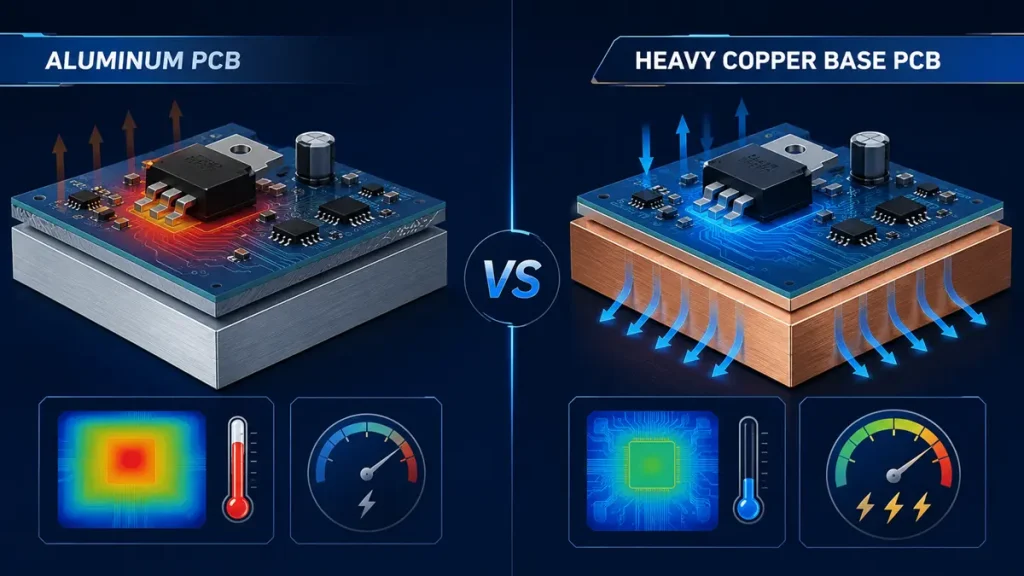
Thermal Performance and Current Density Comparison Between Aluminum PCB and Heavy Copper Base PCB
The generational gap between the two is not cosmetic. Aluminum substrates trade off
thermal conductivity for cost, typically sitting in the 1–3 W/m-K range once the dielectric
layer is factored in. Copper base constructions, by contrast, exist specifically to push heat
dissipation and current-carrying capacity far beyond what an aluminum core can offer,
which is exactly why the raw material and processing costs climb so sharply.
The Three Cost Pillars Behind Every Copper Base PCB Quotation
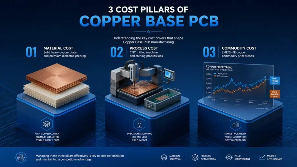
The Three Structural Cost Drivers (Material, Processing, and Commodity Markets) Behind Copper Base PCB Quotations.
Three structural cost drivers explain why a copper base PCB quote rarely looks like a
standard FR4 or aluminum quote:
1. Raw material weight and dielectric grade. Solid copper plate is heavy and priced by
the kilogram, and the imported high-thermal-conductivity prepreg (PP) layer bonding the copper to the circuit layer can represent 70–80% of total material cost on premium builds.
2. Processing loss on thick copper. Etching compensation for heavy copper, accelerated
wear on carbide tooling, and the machine time required for controlled-depth milling
all add labor hours that thinner boards never require.
3. Commodity price exposure. Because copper is priced against LME and SHFE benchmarks, a quotation’s validity window is directly tied to how the raw metal market is moving that week — a detail many first-time buyers overlook when comparing quotes issued days apart.
Five Core Technical Variables That Determine Copper Base PCB Pricing
Buyers who understand these five variables can read a quotation instead of just reacting to
the total at the bottom.
Thermal Conductivity Matrix and Material Brand Selection
Domestic standard dielectric materials typically deliver 1–2 W/m-K, while internationally
recognized brands such as Bergquist and Laird push into the 3–8 W/m-K range and beyond.
The right choice depends entirely on the end application — an AI server power module or
an automotive-grade inverter may genuinely need the premium tier, while over-specifying
thermal grade for a lower-duty design is a common and avoidable source of budget overrun.
Direct Thermal Path (DTP) Construction: Pedestal and Coin Base Technology
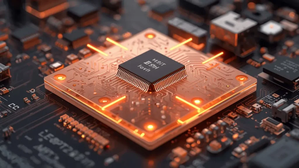
Advanced Direct Thermal Path (DTP) Pedestal Structure Supporting High-Power Electronic Components.
Direct Thermal Path — built through pedestal structures or embedded coin bases — allows
a component to sit in near-direct contact with the copper base, achieving thermal
resistance figures approaching 380 W/m-K. This near-zero thermal resistance is genuinely
transformative for high-power applications, but the added machining precision typically
raises processing cost by 30–50% over a standard dielectric-layer construction.
Heavy Copper PCB Fabrication From 2oz to 10oz and Beyond
Copper weight follows a stepped pricing curve, not a linear one. Moving from a routine 2oz
build to 6oz or beyond 10oz introduces compounding cost: wider etching tolerances are
needed to prevent edge exposure, and heavy copper boards frequently require multiple
passes of solder mask printing to seal against air pockets and copper bleed-through at
conductor edges — a hidden line item that rarely appears explicitly on a quote.
Outline Processing Challenges Unique to Copper Substrates
Standard V-cut separation, routine on FR4 panels, is not a viable option on a solid copper
base — the material is simply too ductile and too thick for a clean V-groove break.
Fabricators instead rely on CNC milling, dedicated stamping dies, or laser cutting, and the
most cost-efficient method depends heavily on order volume: stamping dies pay for
themselves only at higher quantities, while CNC and laser routing remain the sensible
choice for prototypes and small batches.
Hybrid Multilayer Copper Base PCB and Lamination Precision
Some designs combine multilayer FR4 signal layers with a copper-base thermal layer in a
single hybrid stack-up. Getting the lamination alignment right across dissimilar materials
directly affects both registration accuracy and yield rate, and this hybrid complexity is one
of the fastest-growing segments of the copper base PCB category as power electronics
designs get denser.
Prototype vs Mass Production: Where the Real Cost Structure Differs
The Hidden Cost Layers Inside Copper Base PCB Prototyping
A prototype run carries cost categories that never scale proportionally: CAM and DFM
engineering fees, high-density flying-probe test charges, and material utilization losses
from panels that can’t be tiled efficiently at low quantities. This is precisely why a single
prototype copper base PCB can price out at three to five times the per-unit cost of the same
design in mass production — a ratio that surprises many buyers seeing a copper quote for
the first time.
Economies of Scale and Risk Management in Mass Production Runs
At volume, fixed costs such as stamping or profiling tooling and dedicated E-test fixtures
amortize across thousands of units instead of dozens. Larger orders also open the door to
quarterly price-lock agreements, which let both buyer and supplier hedge against short
term copper price volatility rather than repricing every purchase order against the spot
market.
How to Avoid Low-Price Traps When Sourcing a Copper Base PCB Manufacturer
Material Substitution Risk: Why the Contract Needs to Name the Brand
The single most common quality shortcut in this category is quiet substitution of the
dielectric layer — swapping a specified brand like Bergquist T-Clad for an unbranded,
lower-conductivity adhesive that looks identical on paper but underperforms in the field.
Naming the exact substrate brand and thermal layer thickness in the purchase contract
closes this loophole before production starts.
Reading a Copper Base PCB Quotation Without Getting Surprised Later
A quote that looks unusually low is frequently a “bare board” price with testing fees, tooling
charges, and international packaging or freight stripped out and billed separately
afterward. Asking for a fully itemized breakdown before comparing suppliers side by side is
the fastest way to catch this.
DFM Collaboration Can Legitimately Lower Copper Base PCB Cost
Bringing a manufacturer into the design-for-manufacturability conversation early — rather
than after Gerber files are frozen — routinely allows small adjustments to trace width and
spacing that reduce process-difficulty surcharges by roughly 15%, without touching the
electrical performance of the board.
Copper Base PCB Manufacturing Technology in 2026: What Has Changed
The copper base PCB category has moved noticeably in the last two years, driven largely by
demand from AI server power delivery, EV traction inverters, and high-density LED
lighting. A few shifts are worth tracking heading into 2026:
1. AI-assisted DFM screening is increasingly used ahead of quoting, catching clearance
and thermal-pad conflicts before a board reaches the CAM engineer’s desk, which
shortens the quote-to-PO cycle for complex hybrid stack-ups.
2. Higher-performance thermal interface materials in the 6–10 W/m-K range are
becoming more accessible outside the traditional premium-brand-only tier, giving
mid-volume buyers a genuine option between economy and top-tier thermal grades.
3. Tighter tolerance heavy copper etching, supported by improved compensation
software, is narrowing the gap between what 6oz and 10oz copper builds used to cost
versus what they cost today.
4. Demand growth from power electronics and new energy vehicles is pushing hybrid
multilayer copper base construction from a niche request into a standard catalog
offering at established fabricators.
Copper Base PCB DFM Checklist Before Submitting Your RFQ
Use this checklist before sending Gerber files to any supplier — it is the fastest way to avoid
the back-and-forth clarification emails that delay quoting:
1. Does the Gerber package include a dedicated outline layer clearly marking controlled
depth milling or pedestal zones?
2.Is the thermal pad requiring direct contact with the copper base explicitly labeled on the
drawing?
3. For copper weight ≥3oz, has adequate clearance compensation been added to prevent
micro-shorts from incomplete etching?
4.Are high-heat-dissipation zones marked for a wide solder mask opening?
5. Are the commercial boundaries clear — quantity (sample vs. production PO), acceptance
standard (IPC-A-600 Class 2 or Class 3), compliance requirements (RoHS/REACH), and
delivery terms (FOB/EXW/DDP)?
Why Buyers Choose Shenzhen Hongda Circuit Technology for Copper Base PCB Sourcing
Shenzhen Hongda Circuit Technology Co., Ltd. works from the same cost logic laid out
above — transparent, itemized quoting, named substrate brands on every contract, and in
house DFM review before a job enters CAM. For buyers comparing copper base PCB
manufacturers on price alone, that transparency is often the difference between a quote
that holds up through production and one that doesn’t.
To get a quotation, send your Gerber files, BOM, and technical parameter sheet to
sales@pcbkr.com. A senior CAM engineer reviews submissions for DFM issues and
returns a detailed quotation within 24 hours.
Frequently Asked Questions From Buyers Sourcing a Copper Base PCB Supplier
How do I verify that a copper base PCB manufacturer isn’t substituting a lower-grade
thermal material?
Ask the supplier to name the specific dielectric brand and thickness in
writing, and request it be written into the purchase contract or PO, not just the quotation email. Reputable manufacturers, including Shenzhen Hongda Circuit Technology, will provide the material data sheet for the exact brand used on your order.
Why is my copper base PCB prototype quote so much higher per unit than the mass production price?
Prototype pricing carries CAM engineering, flying-probe testing, and
low panel-utilization costs that don’t scale down proportionally at low quantities. A 3–5x per-unit premium versus mass production is standard across the industry, not specific to one supplier.
What’s the real difference between an aluminum MCPCB and a copper base PCB, and how do I know which one my design needs?
Aluminum MCPCB suits low-to-mid power applications where cost matters more than extreme thermal performance. Copper base PCB is worth the added cost when your design involves high current density or heat loads
that aluminum’s lower thermal conductivity genuinely cannot manage — a supplier’s applications engineer can confirm which category your thermal budget actually requires.
What should be included in a copper base PCB quotation so I’m not surprised by extra charges later?
A complete quote should separately itemize the bare board cost, testing fees (including flying-probe or E-test fixture charges), tooling costs for prototypes or low volumes, and packaging/freight terms. If a quote is silent on these, ask for a revised breakdown before comparing it to other suppliers.
How can I reduce copper base PCB manufacturing cost without lowering quality?
The most reliable lever is early DFM collaboration — sharing your design with the manufacturer before finalizing Gerber files often reveals trace width or clearance adjustments that lower process-difficulty surcharges by around 15%, with no impact on thermal or electrical performance.
About Author
David Chen https://www.linkedin.com/in/pcbcoming
David Chen boasts an extensive professional background in PCBA manufacturing, PCBA testing, and PCBA optimization, with specialized expertise in high-precision PCBA fault analysis and rigorous PCBA reliability testing. The author has worked with high-layer-count server PCB fabrication, ultra-low-loss backplane stackups, and thermo-mechanical reliability optimization for AI infrastructure projects involving 112G and 224G PAM4 architectures. Skilled in complex circuit design and cutting-edge advanced PCB manufacturing processes, he delivers solutions that elevate product durability and performance across industrial applications. His technical articles focusing on PCBA manufacturing workflows and testing methodologies are widely cited by industry peers, research institutions, and technical platforms, solidifying his reputation as a recognized technical authority in the global circuit board manufacturing sector.