CXL Expansion Card PCB Manufacturing: Stackup, Signal Integrity, and Supplier Selection
CXL Expansion Card PCB Manufacturing: A CXL expansion card PCB must meet the electrical, mechanical, and thermal requirements of its intended Compute Express Link (CXL) interface and host platform. Successful manufacturing depends on the approved stackup, impedance control, via structures, connector geometry, material consistency, and production validation. Buyers should evaluate these factors against their actual card design before selecting a PCB manufacturer or requesting a quotation.
What Is a CXL Expansion Card PCB and Where Is It Used?
A CXL expansion card PCB is the printed circuit board used in an expansion-card design that implements Compute Express Link connectivity. Depending on the device architecture, it may support memory expansion, accelerator connectivity, or other compute and memory-related functions within a compatible system.
CXL is designed to support coherent communication between processors and connected devices. It uses the PCI Express physical and electrical infrastructure while providing protocol capabilities defined by the relevant CXL specification. However, the PCB requirements of a particular card depend on its interface generation, device architecture, electrical design, and mechanical form factor.
Typical application categories include:
- Memory expansion: Devices that provide additional memory capacity to compatible host platforms.
- Compute acceleration: Expansion cards connecting supported accelerators or other devices to a host.
- Data-center infrastructure: CXL-enabled platforms designed for memory sharing, pooling, or composable computing.
- Specialized computing systems: Systems that require CXL connectivity for a defined workload or platform architecture.
Not every CXL device uses the same expansion-card design. A memory device, accelerator, and other CXL endpoint can have different component layouts, power requirements, routing constraints, and thermal demands. The PCB manufacturer should therefore work from the actual fabrication package rather than assume that one generic CXL stackup fits every application.
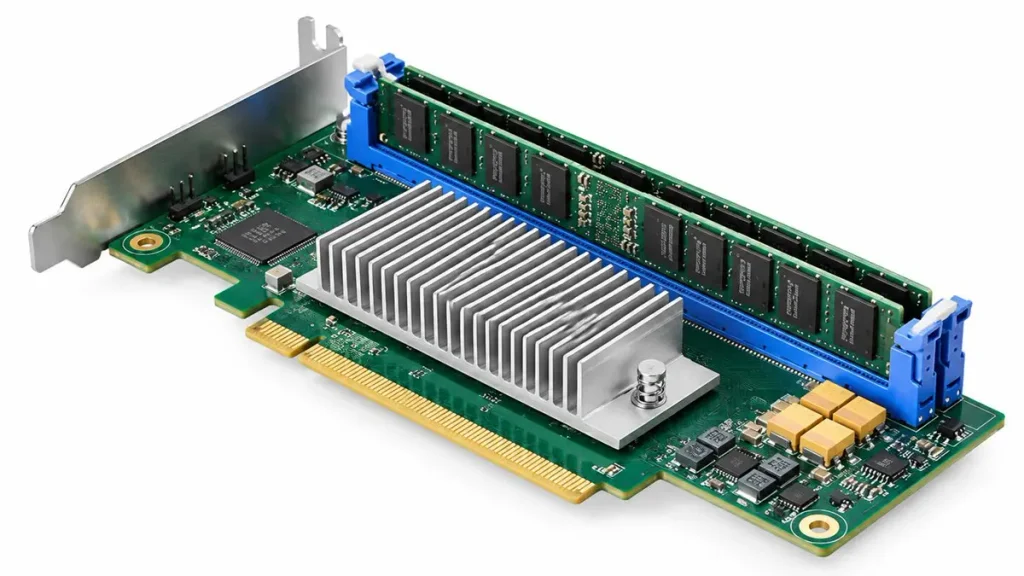
A CXL expansion card PCB combines high-speed routing, component placement, and host-interface connectivity within the mechanical constraints of the target platform.
Which PCB Specifications Should Buyers Confirm Before Requesting a CXL PCB Quote?
Buyers should confirm the released design data, stackup, electrical requirements, mechanical dimensions, and acceptance criteria before requesting a production quotation. These inputs allow the manufacturer to assess fabrication feasibility and identify missing information before pricing.
The following table summarizes the information procurement and engineering teams should prepare.
| Specification | Information to provide | Why it matters |
|---|---|---|
| CXL interface | Target CXL generation and applicable platform requirements | Establishes the design context and electrical validation requirements |
| Layer count | Approved layer count and layer-function definition | Determines routing capacity and stackup complexity |
| PCB thickness | Finished thickness and tolerance | Affects mechanical fit and connector compatibility |
| Base material | Approved laminate manufacturer and material designation, where specified | Helps control dielectric and dimensional characteristics |
| Copper construction | Copper weight or thickness by layer | Affects current capacity, etching, and impedance geometry |
| Controlled impedance | Target impedance by net class, tolerance, and verification requirements | Supports consistent electrical performance |
| Minimum geometry | Required trace width, spacing, annular ring, and clearance | Determines whether the design fits the manufacturer’s process capability |
| Via design | Through vias, blind/buried vias, microvias, and backdrilling requirements | Affects routing density, fabrication sequence, and inspection |
| Mechanical features | Board outline, connector footprint, edge contacts, holes, and cutouts | Supports fit and assembly compatibility |
| Surface finish | Approved finish and contact requirements | Affects solderability or connector-interface requirements |
| Validation | Electrical tests, impedance reports, dimensional inspection, and other required records | Defines acceptance criteria and supplier deliverables |
| Quantity and schedule | Prototype quantity, production demand, target delivery, and shipping destination | Supports realistic cost and delivery planning |
Do not specify universal layer counts, trace widths, or impedance values simply because a board is CXL-enabled. Those values must come from the design, interface requirements, approved stackup, and relevant engineering analysis.
For example, a controlled-impedance requirement should identify the applicable net class and target value rather than state that every trace on the board has the same impedance. Likewise, a request for backdrilling should identify the relevant vias and the applicable manufacturing drawing.
How Should Engineers Select the Stackup and Low-Loss Materials for a CXL Expansion Card PCB?
Engineers should select the stackup and materials according to the electrical channel requirements, routing architecture, mechanical constraints, and manufacturing design rules. A low-loss material may help control transmission loss, but material selection alone does not guarantee acceptable signal integrity.
The stackup defines the arrangement of signal layers, reference planes, dielectric layers, and copper thicknesses. These factors influence impedance, coupling, insertion loss, return loss, crosstalk, and dimensional stability.
Which stackup inputs should be reviewed?
Before approving the stackup, engineering and procurement teams should confirm:
- Layer assignment and the reference plane for each critical signal layer.
- Dielectric thickness and the material properties used for impedance calculations.
- Copper thickness, including the expected finished copper construction.
- Controlled-impedance net classes and their required tolerances.
- Routing density and the space available for reference-plane continuity.
- Via structures and any specified backdrilling.
- Finished board thickness and mechanical tolerances.
- Material availability and approval requirements for substitutions.
A stackup proposal should reflect the actual fabrication process, not only an idealized electrical model. The manufacturer and design team should resolve any differences between the design’s assumed dielectric construction and the material system available for production.
How should low-loss laminate selection be handled?
Material selection should be based on the frequency-dependent electrical requirements and the approved design. Relevant parameters may include dielectric constant, dissipation factor, dielectric thickness, copper roughness, thermal properties, and dimensional stability.
The values used in engineering calculations should correspond to the selected material, test method, frequency, and construction. Published dielectric properties from different test conditions should not be treated as directly interchangeable.
For a design that specifies a particular laminate, the manufacturer should not substitute another material without engineering review and buyer approval. A material change can affect impedance, insertion loss, thickness, lamination behavior, and dimensional stability.
For a broader overview of high-speed PCB fabrication capabilities and design considerations, see High-Speed PCB Manufacturing. This CXL article focuses on how those manufacturing considerations apply to a specific expansion-card project.
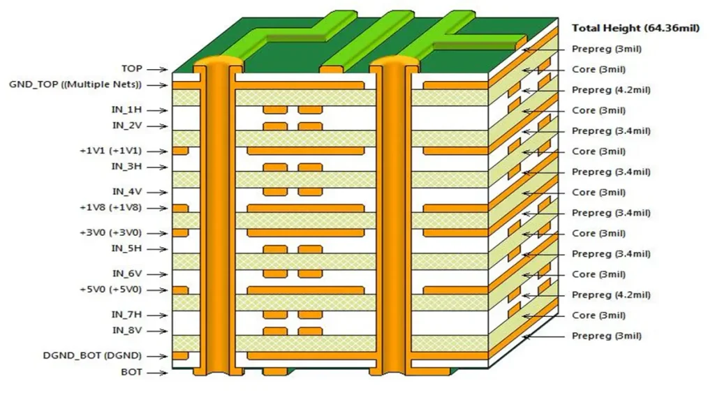
The approved stackup, dielectric construction, copper geometry, and via design should be reviewed together when preparing a CXL expansion card PCB for manufacturing.
How Can PCB Manufacturing Preserve Signal Integrity in CXL Expansion Cards?
Signal integrity depends on both the electrical design and the consistency of the manufactured PCB. The manufacturer’s task is to fabricate the approved geometry and material construction within specified tolerances and provide the agreed verification records.
For a CXL expansion card, important manufacturing considerations include controlled-impedance routing, reference-plane continuity, via structures, copper geometry, and layer registration. The appropriate acceptance criteria depend on the design and its validation plan.
Why does impedance control matter?
The characteristic impedance of a PCB transmission line depends on several interacting variables, including trace width, copper thickness, dielectric thickness, and the dielectric properties of the material system.
If the manufactured geometry differs from the geometry assumed during design, the resulting impedance may also differ. Buyers should therefore confirm that the proposed stackup and fabrication process are compatible with the specified impedance targets.
A practical review should establish:
- Which nets require controlled impedance.
- The target impedance and tolerance for each relevant net class.
- The stackup and material construction used to support the target.
- The supplier’s impedance verification method and reporting format.
- The acceptance criteria and sampling plan for production.
The manufacturer should not invent impedance targets or change the design geometry without authorization. Any proposed adjustment should be reviewed by the responsible engineering team.
When should backdrilling be considered?
Backdrilling may be specified when the design analysis identifies residual via stubs as a concern for high-speed signal paths. It removes unused portions of plated through-holes to reduce the electrical impact of those stubs.
However, backdrilling is not automatically required for every CXL expansion card. Its use depends on the via architecture, routing topology, electrical requirements, and approved design.
Where backdrilling is required, the fabrication package should define the affected vias, drilling direction, target depth or residual stub requirement, and applicable tolerances. The supplier should confirm that the specified process can be supported and explain how the relevant features will be verified.
Which signal-integrity manufacturing risks should buyers review?
| Risk | Potential consequence | Recommended review |
|---|---|---|
| Trace geometry variation | Impedance may differ from the approved design | Confirm the stackup, geometry, process capability, and impedance verification plan |
| Inconsistent dielectric construction | Electrical and dimensional characteristics may change | Confirm the material designation, dielectric thickness, and approved stackup |
| Backdrill depth or position deviation | Residual stubs or unintended copper removal may result | Review backdrill instructions, tolerances, and applicable inspection records |
| Layer-registration variation | Clearances or via-to-pad relationships may deviate from the design | Confirm registration requirements and review first-article results |
| Reference-plane discontinuity in the design or released data | Return paths may be compromised | Review the released routing and reference-plane design before fabrication |
| Unapproved material substitution | Electrical performance may differ from the validated design | Require documented engineering review and written approval |
These are potential failure mechanisms, not a claim that every CXL board will experience them. The acceptance limits should be defined by the approved fabrication drawing, electrical requirements, applicable standards, and project validation plan.
How Should Power Delivery and Thermal Management Be Evaluated on a CXL Expansion Card PCB?
Power delivery and thermal requirements should be evaluated against the actual device architecture, component power consumption, connector limitations, copper construction, and cooling system. A CXL label alone does not determine the board’s current capacity or thermal requirements.
The PCB design may need to accommodate high-speed signals alongside power-distribution networks, voltage-regulation components, memory devices, or other components. The design team should assess voltage-drop limits, current density, copper resistance, thermal spreading, and the placement of heat-generating components.
Before fabrication, buyers should confirm:
- Copper thickness and the layer allocation for power and ground.
- Power-plane and return-path requirements.
- Current-carrying requirements defined by the design.
- Thermal-interface and mechanical-clearance constraints.
- Component placement restrictions around the connector and cooling hardware.
- Any specific board temperature, reliability, or dimensional requirements.
- Whether changes to copper geometry or stackup require renewed electrical or thermal review.
The PCB manufacturer can review manufacturing feasibility, copper construction, spacing, and dimensional requirements. It should not replace the system designer’s power-integrity or thermal analysis unless that engineering service has been explicitly included in the project scope.
Which PCB Manufacturing Processes Matter Most for High-Density CXL Expansion Cards?
The most relevant manufacturing processes are those needed to reproduce the approved stackup, routing geometry, via structures, and mechanical interfaces. The exact process sequence depends on the design’s layer count, interconnection architecture, material system, and required tolerances.
Potentially relevant processes include:
- Imaging and etching: To form the specified copper features and conductor geometry.
- Lamination: To build the multilayer construction while maintaining the specified dielectric arrangement and dimensional stability.
- Drilling and via formation: To create the interconnections defined by the fabrication data.
- Backdrilling: Where required by the approved design.
- Surface finishing: To meet the specified solderability, contact, or assembly requirements.
- Electrical testing: To check the required connectivity and isolation criteria.
- Dimensional inspection: To verify board outline, thickness, holes, and other specified mechanical features.
For high-density designs, the supplier should review the minimum trace and space, via dimensions, layer registration, annular-ring requirements, and material construction before accepting the job. If a design exceeds a supplier’s demonstrated process capability, the issue should be raised during engineering review rather than discovered after production starts.
Advanced equipment can improve process control, but equipment names alone do not prove that a specific design can be manufactured successfully. The relevant evidence is the supplier’s demonstrated capability for the required design features and the verification records agreed for the project.
What Manufacturing Risks Should Buyers Review Before Releasing a CXL Expansion Card PCB?
Buyers should review the gap between the approved design and the physical board that will be manufactured. A structured engineering handoff helps identify potential issues before they affect first-article acceptance or production scheduling.
| Manufacturing risk | Possible impact | What should the buyer request? |
|---|---|---|
| Impedance variation | The finished channel may not match the approved electrical assumptions | Confirm the stackup, impedance targets, and verification method |
| Backdrill deviation | Residual via stubs or unintended copper removal | Review the backdrill drawing, tolerances, and inspection records |
| Layer-registration variation | Clearance, annular-ring, or local geometry issues | Confirm design-specific registration requirements and first-article results |
| Lamination or material variation | Changes in thickness, dimensional stability, or electrical characteristics | Confirm the approved construction and material-substitution process |
| Connector or card-edge mismatch | Mechanical fit or interface problems | Review the approved mechanical drawing and finished-board measurements |
| Conflicting fabrication revisions | The supplier may manufacture from outdated data | Match revision identifiers across fabrication data, drill files, stackup, and drawings |
These checks should be incorporated into the engineering release and acceptance plan. Not every item requires the same inspection method, and not every risk applies to every design.
For wider pre-production design checks involving AI server boards and high-speed interfaces, see the AI Server PCB DFM Checklist. That resource addresses the broader DFM review; this article focuses on applying manufacturing controls to CXL expansion-card projects.
How Can Buyers Verify a CXL PCB Manufacturer’s Capabilities?
Buyers should evaluate a manufacturer against the actual fabrication package, process requirements, and evidence available for the proposed job. General claims such as “high-speed capable” or “advanced PCB manufacturing” are not substitutes for a documented capability review.
Before awarding the order, request confirmation of the following:
- Stackup feasibility: Can the supplier build the proposed layer arrangement, material construction, and finished thickness?
- Impedance control: Can the supplier support the required net classes and provide the agreed verification records?
- Via and drilling capability: Can the required via structures, hole dimensions, and backdrilling instructions be supported?
- Registration and dimensional control: Are the specified mechanical and layer-registration requirements compatible with the supplier’s demonstrated process?
- Inspection and testing: Which dimensional, electrical, impedance, or other inspection records will be supplied?
- Material traceability: Can the supplier identify the material construction used for the production lot when required?
- Revision control: How will the supplier ensure that the approved fabrication files and drawings are used?
- Change management: How are deviations, material substitutions, and process changes documented and approved?
Where possible, review evidence relevant to the actual project, such as a proposed stackup, an impedance-control plan, a sample inspection report, or a first-article record. Confidential customer data need not be disclosed; the supplier can provide appropriately redacted examples where available.
Do not assume that a supplier supports a particular layer count, minimum line width, test frequency, or delivery time unless it has been confirmed for the project.
For broader sourcing considerations, see AI Server PCBs China Supplier. That page supports the wider supplier-selection topic, while this page remains focused on CXL expansion card manufacturing.
What Quality Tests Should Be Included in CXL Expansion Card PCB Validation?
The validation plan should be based on the released drawings, applicable PCB specifications, electrical requirements, and customer acceptance criteria. No single test can establish every aspect of PCB quality.
Depending on the design and procurement specification, the following checks may be appropriate.
| Verification item | What it checks | Important limitation |
|---|---|---|
| Electrical continuity and isolation testing | Required conductive connections and isolation between specified nets | Does not by itself prove high-speed channel performance |
| Controlled-impedance testing | Whether the tested structures meet the specified impedance criteria | Method, test structures, and sampling must be agreed in advance |
| Dimensional inspection | Board outline, thickness, holes, and specified mechanical features | Must use the approved drawing and tolerances |
| Visual inspection or automated optical inspection | Observable copper-pattern and surface-related defects within the method’s scope | Cannot detect every internal or electrical defect |
| Microsection analysis, where specified | Internal construction, plating, and selected structural characteristics | Sampling and acceptance criteria must be defined |
| Material and lot documentation | Traceability to the approved construction, where required | Documentation requirements depend on the purchase specification |
| First-article review | Whether the initial production output conforms to the released requirements | Does not eliminate the need for agreed production controls |
If the design requires additional reliability testing, environmental testing, or high-frequency characterization, those requirements should be specified separately. Such testing should not be assumed to be included in a standard PCB quotation.
Buyers should agree on the test method, sampling plan, report format, and acceptance limits before production begins. Where a report is required for release, the purchase order should identify that deliverable explicitly.
What Factors Determine CXL Expansion Card PCB Cost and Lead Time?
CXL expansion card PCB cost and lead time depend on the design’s manufacturing complexity, material requirements, production quantity, inspection scope, and schedule. The interface name alone is not enough to determine a reliable price or delivery date.
Common cost drivers include:
- Layer count and overall stackup complexity.
- Material type, availability, and required construction.
- Minimum trace width, spacing, and via dimensions.
- Blind, buried, or microvia structures, where specified.
- Backdrilling and other additional process steps.
- Finished board thickness and copper construction.
- Surface finish and mechanical processing.
- Required impedance verification, inspection, and documentation.
- Prototype quantity, repeat-order volume, and panel utilization.
- Engineering review, data clarification, and first-article approval.
Lead time can also be affected by material procurement, engineering questions, fabrication complexity, testing, and shipping. A quotation should distinguish the manufacturing lead time from transit time and identify assumptions that could affect the schedule.
To obtain a useful quotation, provide complete and revision-controlled fabrication data. If the stackup or material is still under review, ask the supplier to identify which quotation assumptions remain provisional.
A low initial price may not represent the lowest total project cost if the quotation excludes required tests, documentation, special processing, or engineering review. Buyers should compare quotations against the same technical scope and acceptance criteria.
How Can Buyers Prepare an RFQ for CXL Expansion Card PCB Manufacturing?
A complete request for quotation (RFQ) should include the files and requirements needed to assess manufacturability, price, validation, and delivery. Missing or conflicting information can lead to clarification delays or quotations based on different assumptions.
Use this checklist when preparing a CXL expansion card PCB RFQ.
PCB fabrication data
- Gerber or ODB++ files, as applicable.
- NC drill files and separate backdrill data or drawings, if required.
- Approved stackup and layer-function definition.
- Material designation and copper construction.
- Finished board thickness and tolerance.
- Board outline, cutouts, holes, and connector/card-edge details.
- Surface-finish requirements.
- Controlled-impedance table and relevant fabrication notes.
Quality and validation requirements
- Required electrical continuity and isolation tests.
- Impedance verification requirements, including reporting expectations.
- Dimensional inspection and first-article requirements.
- Any required material or lot documentation.
- Applicable product specifications and acceptance criteria.
- Special reliability, cleanliness, or environmental requirements, where applicable.
Commercial and scheduling information
- Prototype quantity and expected production volume.
- Target delivery date and shipping destination.
- Packaging and handling requirements.
- Current revision identifiers and the authorized contact for engineering questions.
- A list of any parameters that remain open for review.
- Requirements for written approval of material substitutions or manufacturing deviations.
If the design is not fully released, clearly separate confirmed requirements from provisional parameters. This helps the supplier identify the decisions needed before a production-ready quotation can be issued.
Request a CXL Expansion Card PCB Manufacturing Review
Shenzhen Hongda Circuit Technology Co., Ltd. welcomes inquiries from engineering and procurement teams evaluating PCB fabrication for CXL expansion cards.
Send your fabrication data, stackup requirements, impedance specifications, target quantities, and schedule to pcb@pcbkr.com or visit PCBKR. The information will help define the manufacturing scope and identify any engineering details that need clarification before quotation.
Any proposed material, stackup, or process change should be reviewed and approved by the responsible engineering team before production.
Frequently Asked Questions About CXL Expansion Card PCB Manufacturing
What files are required for a CXL expansion card PCB quote?
Provide the PCB fabrication data, drill files, approved stackup, material requirements, impedance table, mechanical drawings, quantities, and target schedule. Include backdrill instructions and special inspection requirements where applicable.
Does every CXL expansion card PCB require backdrilling?
No. Backdrilling depends on the via design, channel requirements, and engineering analysis. The manufacturer should follow the released fabrication data and approved instructions rather than assume it is required for every design.
How can buyers verify impedance control for a CXL expansion card PCB?
Confirm the target impedance values, tolerances, applicable net classes, and acceptance criteria before fabrication. Then agree on the supplier’s verification method, test structures where applicable, sampling plan, and report format.
Can a PCB manufacturer replace the specified low-loss material with an alternative?
A material substitution should not be made without appropriate engineering review and buyer approval. Changes can affect dielectric properties, thickness, dimensional stability, lamination behavior, and electrical performance
What should buyers review before approving the first production lot?
Review the approved design revision, stackup and material records, dimensional inspection, relevant electrical test results, impedance reports where specified, and documented resolution of manufacturing deviations.
Which PCB parameters have the greatest effect on CXL expansion card manufacturing cost?
Layer count, material construction, minimum geometry, via complexity, backdrilling, board thickness, surface finish, inspection scope, quantity, and schedule can all affect cost. The relative impact depends on the actual fabrication package.
Can a standard high-speed PCB manufacturer fabricate a CXL expansion card PCB?
Possibly, but the supplier should be evaluated against the specific design requirements. Confirm stackup feasibility, controlled-impedance capability, via processing, mechanical tolerances, testing, and documentation before placing an order.
What should be included in the PCB manufacturer’s quotation?
The quotation should identify the proposed material and stackup assumptions, fabrication scope, quantity, price, manufacturing lead time, included inspection and testing, required customer inputs, and any exclusions or unresolved technical questions.
How can buyers reduce delays during CXL PCB procurement?
Provide complete, revision-controlled fabrication files, clearly defined electrical and mechanical requirements, an agreed acceptance plan, and a single process for resolving engineering questions. Approving the stackup and material assumptions early can also reduce avoidable clarification cycles.
Should the PCB manufacturer validate the complete CXL channel?
PCB fabrication validation and complete channel validation are different responsibilities. The manufacturer can provide agreed fabrication and electrical verification records, but system-level channel validation may require additional design analysis, test structures, equipment, and work by the responsible hardware engineering team.
Conclusion
CXL expansion card PCB manufacturing requires alignment between the released electrical design, approved material construction, fabrication process, mechanical interfaces, and validation plan. Buyers can reduce procurement risk by confirming the stackup, controlled-impedance requirements, via structures, material restrictions, inspection records, and revision controls before production.
For Shenzhen Hongda Circuit Technology Co., Ltd., the appropriate starting point for a project discussion is the customer’s actual fabrication package and acceptance requirements. A clear RFQ enables a more meaningful manufacturability review and a quotation based on defined technical and commercial assumptions.
About Author
David Chen (G) LinkedIn Profile
David Chen is a Senior RF/PCB Process Engineer at Shenzhen Hongda Circuit Technology Co., Ltd., with over 12 years of experience in high-frequency PCB fabrication, impedance-controlled stack-up design, and Rogers/PTFE laminate processing. He also boasts an extensive professional background in PCBA manufacturing, PCBA testing, and PCBA optimization, with specialized expertise in high-precision PCBA fault analysis and rigorous PCBA reliability testing. The author has worked with high-layer-count server PCB fabrication, ultra-low-loss backplane stackups, and thermo-mechanical reliability optimization for AI infrastructure projects involving 112G and 224G PAM4 architectures. Skilled in complex circuit design and cutting-edge advanced PCB manufacturing processes, he delivers solutions that elevate product durability and performance across industrial applications. His technical articles focusing on PCBA manufacturing workflows and testing methodologies are widely cited by industry peers and technical platforms, and have gained attention and recognition from industry colleagues.