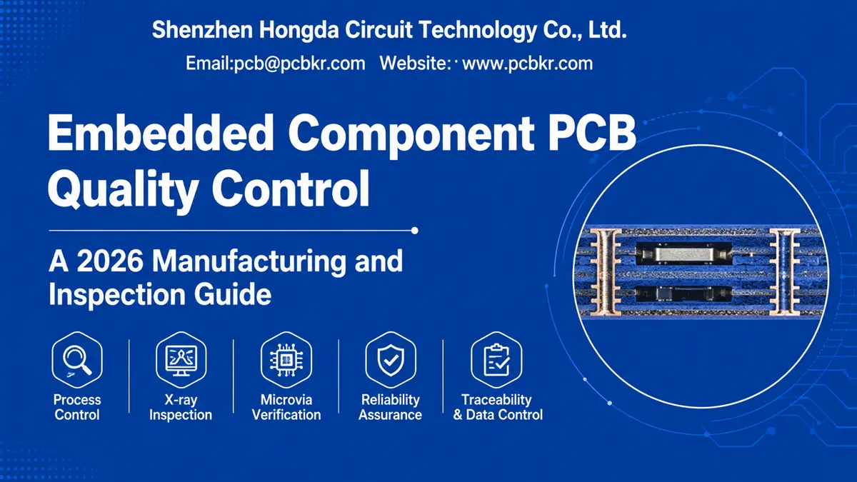
Embedded Component PCB Quality Control: An Advanced Manufacturing and Inspection Guide
Embedded component PCB quality control requires process‑level control from material receiving through component placement, cavity machining, lamination, laser microvia formation, plating, inspection, electrical testing, and lot traceability. The critical difference is that many internal defects become inaccessible after lamination, so manufacturers must verify hidden structures before they are permanently sealed.
For Shenzhen Hongda Circuit Technology Co., Ltd., embedded‑component PCB quality control should therefore be treated as a manufacturing‑system problem rather than a final‑inspection problem.
A reliable production strategy combines dimensional measurement, placement verification, AOI/3D inspection, X‑ray inspection, microsection analysis, electrical testing, process SPC and complete production traceability.
Why Is Embedded Component PCB Quality Control More Difficult Than Conventional PCB Inspection?
Embedded PCB inspection is more difficult because components, cavities, internal copper structures and microvias can become physically inaccessible after lamination.
A conventional PCB allows inspectors to visually examine most external features after fabrication.
An embedded component PCB is different.
Depending on the construction, critical structures may include:
‑ Embedded passive components ‑ Embedded active components ‑ Internal cavities ‑ Copper‑filled microvias ‑ Blind and buried vias ‑ Internal copper planes ‑ Component‑to‑via connections ‑ Lamination interfaces ‑ Internal dielectric layers ‑ Fine‑line HDI structures
The quality‑control problem is therefore visibility loss.
Once the board has been laminated, an operator may no longer be able to directly see whether:
‑ the component shifted; ‑ the cavity wall was damaged; ‑ resin completely filled the surrounding area; ‑ a void formed beside the component; ‑ a microvia landed correctly; ‑ copper plating contains a defect; ‑ internal registration moved outside the engineering tolerance.
This is why the original manufacturing principle remains important:
Do not wait until final inspection to discover a defect that should have been controlled before lamination.
IPC’s current rigid‑board framework specifically includes multilayer boards with blind/buried vias/microvias and active/passive embedded circuitry. IPC‑6012F also expanded requirements relating to cavities, hole registration, internal plated layers and microvia reliability. For end‑to‑end technology overview, design challenges and supplier qualification workflows for embedded‑component projects, please refer to our Embedded Component PCB: Technology, Manufacturing & Procurement Guide.
What Should a Manufacturer Check Before Starting Embedded PCB Production?
Incoming inspection should verify the PCB materials, copper foil, embedded components, component dimensions, electrical values, material specifications and lot information before fabrication begins.
The incoming inspection stage should establish a controlled baseline.
Recommended incoming inspection matrix
| Control item | Typical engineering parameter | Verification method |
|---|---|---|
| Component length/width | According to component drawing | Optical measurement |
| Component thickness | According to component drawing | Digital micrometer / vision |
| Component electrical value | Design nominal ± component tolerance | LCR / electrical tester |
| Material grade | Approved material specification | CoC + material record |
| Copper foil | Specified Cu weight/thickness | Supplier documentation + measurement |
| Component lot | 100% traceable | Barcode / ERP / MES |
| Dielectric material | Approved laminate/prepreg | CoC + incoming inspection |
| Moisture condition | Supplier‑controlled | MSL/material handling procedure |
Component dimensional consistency is especially important because the cavity is not an independent feature.
It is effectively a mechanical envelope designed around the component.
If the actual component thickness is different from the value used in the PCB design, the problem can appear later as:
component variation → cavity clearance variation → resin‑flow variation → local stress → lamination deformation.
That is a manufacturing chain, not an isolated dimensional error.
How Should Embedded PCB Cavities Be Measured and Controlled?
Cavity quality should be controlled by measuring X/Y dimensions, depth, position, wall condition, surface condition and component clearance—not simply by checking whether the cavity matches its nominal CAD dimensions.
For a cavity, I recommend separating the control parameters into six groups:
- Length
- Width
- Depth
- X/Y position
- Wall condition
- Component clearance
A practical production control sheet can therefore use:
| Parameter | Engineering control |
|---|---|
| Cavity X | CAD nominal + drawing tolerance |
| Cavity Y | CAD nominal + drawing tolerance |
| Depth | Drawing‑defined tolerance |
| Position | Datum/reference‑based |
| Wall roughness | Process‑dependent |
| Burr/residue | Not permitted where it interferes with placement |
| Component clearance | Defined during DFM |
| Bottom copper condition | Verified before component insertion |
The manufacturing pain point
The most common mistake is treating a cavity as a simple milling feature.
It is not.
A cavity interacts with:
‑ component thickness; ‑ adhesive thickness; ‑ dielectric thickness; ‑ prepreg resin flow; ‑ copper distribution; ‑ lamination pressure; ‑ vacuum; ‑ subsequent laser drilling; ‑ final board thickness.
A cavity that looks acceptable under a microscope can still produce a poor laminated structure if the component‑to‑cavity clearance and resin‑flow window are not properly controlled.
This is why the source article correctly identifies cavity compatibility with the component and subsequent lamination process as more important than nominal cavity dimensions alone.
How Can Component Placement Accuracy Be Verified Before Lamination?
Embedded component placement should be verified using optical alignment, fiducials, X/Y measurement, orientation inspection, pre‑lamination inspection and X‑ray where the structure requires internal verification.
The critical parameter is internal registration.
For example, consider an embedded component whose terminals must connect to subsequent microvias.
A placement shift does not necessarily create an immediate visible defect.
Instead:
component shift → terminal shift → via landing reduction → annular‑ring loss → electrical/reliability risk.
This is why placement must be checked against the actual downstream via structure, rather than judged only by whether the component remains inside the cavity.
Recommended placement‑control data
A production report should ideally record:
‑ X coordinate ‑ Y coordinate ‑ rotation angle ‑ component orientation ‑ fiducial reference ‑ component lot ‑ operator/machine ID ‑ inspection result ‑ panel number ‑ timestamp
For high‑density embedded structures, the engineering drawing should define the relevant datum scheme before production.
IPC’s design and performance framework emphasizes that procurement documentation needs to provide sufficient information for the supplier to fabricate and verify the desired board.
What Are the Biggest Lamination Quality Problems in Embedded Component PCBs?
The major lamination risks are resin starvation, internal voids, component movement, excessive resin flow, thickness variation, warpage, local stress concentration and incomplete bonding around embedded structures.
Lamination is one of the highest‑risk stages because it permanently closes access to the embedded structure.
Parameters that should be monitored
‑ Lamination temperature ‑ Pressure profile ‑ Vacuum level ‑ Heating rate ‑ Cooling rate ‑ Resin flow ‑ Press cycle ‑ Final board thickness ‑ Warpage ‑ Panel construction ‑ Copper distribution ‑ Prepreg selection
The original article identifies temperature, pressure, vacuum, resin flow, thickness, warpage and internal voids as core lamination‑control parameters.
A practical engineering warning
Do not evaluate lamination only by:
“The final thickness is within tolerance.”
A board can achieve the correct overall thickness while still containing:
‑ local resin starvation; ‑ internal voids; ‑ component edge stress; ‑ delamination; ‑ insufficient dielectric coverage; ‑ localized warpage.
For embedded PCBs, global thickness is not equivalent to internal structural quality.
How Should Microvias and HDI Structures Be Inspected in Embedded Component PCBs?
Microvia quality should be verified through AOI/3D inspection, X‑ray where appropriate, microsection analysis and electrical testing, with special attention to via landing, copper fill, registration and interconnection reliability.
Modern embedded‑component designs increasingly combine embedded devices with HDI structures.
That introduces another failure mechanism:
embedded component position → dielectric build‑up → laser drilling → microvia landing → copper plating → electrical connection.
IPC defines microvia technology within the HDI ecosystem, and IPC’s current standards work continues to address advanced HDI and ultra‑HDI manufacturing.
For reference, an IPC technical resource describes a microvia as a blind hole with diameter up to 150 μm, while advanced manufacturing can go substantially finer depending on the process, material system and customer specification.
What engineers should actually inspect
Do not only ask:
“Is the microvia present?”
Ask:
‑ Did the laser hit the intended target? ‑ Is the landing sufficient? ‑ Is the dielectric thickness controlled? ‑ Is copper plating continuous? ‑ Is the via fill complete where required? ‑ Is there a void? ‑ Is there a crack at the interface? ‑ Is the stacked‑via structure mechanically reliable? ‑ Is the electrical resistance stable?
IPC’s current acceptance and performance ecosystem specifically recognizes microvia target landing and copper‑filled vias as inspection considerations.
Which Inspection Technologies Should Be Used for Hidden Embedded Structures?
No single inspection method is sufficient; the most robust approach combines AOI, 3D inspection, X‑ray, microsection/cross‑section and electrical testing according to the structure’s risk.
A practical inspection chain is:
AOI → 3D Inspection → X‑Ray → Cross‑Section → Electrical Test
Each method answers a different engineering question.
| Inspection | Best suited for |
|---|---|
| 2D AOI | External pattern defects |
| 3D inspection | Height/profile/geometry |
| X‑ray | Hidden component and internal connection inspection |
| Cross‑section | Internal copper, via and lamination structure |
| Electrical test | Opens, shorts and connectivity |
| Dimensional measurement | Cavity/board geometry |
| SPC | Process stability |
| Traceability | Root‑cause investigation |
The original source uses essentially this same inspection hierarchy because hidden defects cannot reliably be detected by one technology alone.
Manufacturing Improvement: 3D Digital DFMP
One important development is the increasing use of 3D manufacturing‑aware DFM.
Siemens’ 2025 Valor NPI update, for example, added a 3D viewer capable of measuring distances in three‑dimensional space and clarifying embedded‑component layer placement.
This is particularly relevant to embedded PCB production because a traditional 2D DFM review can miss spatial relationships between:
‑ cavity; ‑ component; ‑ copper; ‑ via; ‑ neighboring layer; ‑ keep‑out area.
How Can AI and Automated Inspection Improve PCB Quality Control ?
AI‑assisted inspection can improve defect classification, reduce unnecessary manual review and connect inspection results with production traceability, but it should supplement—not replace—engineering validation.
Modern electronics manufacturing is moving from simple inspection toward data‑driven quality control.
AI/computer‑vision systems can analyze production images and identify patterns that are difficult to classify consistently through manual inspection.
Siemens reports that AI‑based component analytics can use images generated during placement to support component authenticity and traceability, while AI‑based AOI false‑call reduction can distinguish potential false calls from real defects.
This matters because excessive false calls create another manufacturing problem: inspection fatigue.
A published Siemens case study reported an AOI first‑pass yield of 60%, with 97.5% of the remaining calls classified as false calls in that particular production environment.
For embedded PCB manufacturing, however, AI should never be used as an excuse to eliminate destructive verification.
A sophisticated quality system still needs:
AI inspection + X‑ray + cross‑section + electrical verification + engineering review.
Why Is Cross‑Section Analysis Still Important for Advanced Embedded PCBs?
Cross‑section analysis remains one of the most valuable engineering verification methods because it directly exposes internal copper, dielectric, microvia and lamination structures that surface inspection cannot fully verify.
For complex embedded PCBs, a cross‑section can reveal:
‑ copper thickness; ‑ plated‑hole structure; ‑ microvia geometry; ‑ via fill; ‑ voids; ‑ dielectric thickness; ‑ component interface; ‑ resin distribution; ‑ delamination; ‑ internal registration; ‑ copper‑to‑copper interfaces.
IPC‑6012F includes microsection evaluation and expanded requirements associated with internal plated layers and microvia reliability.
Expert engineering perspective
A cross‑section should not be treated as merely a customer‑report photograph.
The real value is process feedback.
If three consecutive lots show similar microvia deformation, the question is not:
“Can we pass this board?”
The engineering question should be:
“Which process variable is producing the same structural signature repeatedly?”
That difference separates inspection from process engineering.
What Traceability Data Should an Embedded PCB Manufacturer Keep?
Each production lot should be traceable to material lots, component lots, manufacturing batches, lamination records, inspection results, electrical‑test results and nonconformance records.
A useful traceability architecture is:
Material Lot → Panel ID → Component Lot → Placement Data → Lamination Recipe → Laser Process → Plating Batch → Inspection → Electrical Test → Shipment
At minimum, records should include:
‑ PCB material lot ‑ Copper foil lot ‑ Prepreg lot ‑ Embedded component lot ‑ Production batch ‑ Panel number ‑ Lamination cycle ‑ Inspection results ‑ X‑ray records where applicable ‑ Cross‑section records ‑ Electrical test result ‑ NCR/nonconformance record ‑ Rework record ‑ Final disposition
The original document correctly identifies material lots, component lots, manufacturing batches, lamination records, inspection results, electrical results and nonconformance records as important traceability elements.
Why does procurement care?
Because a supplier should be able to answer:
“Which manufacturing conditions produced this specific board?”
rather than simply:
“We inspected it and it passed.”
How Should Yield Be Used to Evaluate an Embedded PCB Supplier?
Yield should be evaluated as a process‑stability indicator, not merely as a production‑cost metric.
For procurement, one supplier may say:
“We can manufacture your embedded PCB.”
A more important question is:
“Can you manufacture it consistently at production volume?”
That distinction is critical.
Recommended yield KPIs
A supplier evaluation can track:
‑ First‑pass yield (FPY) ‑ Final yield ‑ Scrap rate ‑ Rework rate ‑ Cavity defect rate ‑ Placement defect rate ‑ Lamination defect rate ‑ Microvia defect rate ‑ Electrical‑test failure rate ‑ Customer‑return rate ‑ Lot‑to‑lot variation
For example, if:
Lot A = 97.8% yield Lot B = 98.1% yield Lot C = 97.9% yield
the process appears relatively stable.
But if:
Lot A = 99.1% Lot B = 96.4% Lot C = 92.7%
the average yield alone hides a serious process‑control problem.
The source article makes this same distinction: production yield is a meaningful indicator separating laboratory capability from repeatable manufacturing capability.
What Are the Most Expensive Manufacturing Pain Points in Embedded Component PCB Production?
The most expensive problems usually occur when a defect is allowed to move from an inexpensive upstream inspection stage into a later irreversible process such as lamination, plating, assembly or final test.
Pain point 1: Component dimensional variation
A small component‑thickness difference can change cavity clearance and lamination behavior.
Pain point 2: Placement shift
A component can remain inside its cavity while still becoming misaligned with a subsequent microvia.
Pain point 3: Resin‑flow uncertainty
Insufficient or excessive resin flow can create internal structural problems.
Pain point 4: Hidden voids
A void may remain invisible after lamination and become apparent only through X‑ray, cross‑section or reliability testing.
Pain point 5: Microvia reliability
As HDI structures become finer, registration and interconnection reliability become increasingly sensitive to process variation.
Pain point 6: Excessive false calls
Poorly optimized automated inspection can consume engineering resources without improving real defect detection.
Pain point 7: Weak traceability
If the manufacturer cannot associate a defect with a specific material lot, machine condition or lamination cycle, root‑cause analysis becomes slow and expensive.
Pain point 8: Yield instability
A prototype can pass while mass production fails because the process window is too narrow.
This is precisely why IPC’s newer rigid‑board requirements have expanded attention to cavities, registration, microvia reliability and structural verification.
Which PCB Manufacturing Technologies Are Most Relevant to Embedded Component Quality?
The most relevant technologies are high‑precision cavity machining, HDI laser microvia processing, copper‑filled microvias, advanced registration control, 3D DFM, automated optical inspection, X‑ray inspection, AI‑assisted inspection, digital traceability and structured process SPC.
The important point is that technology should be selected according to failure mode.
| Technology | Quality‑control value |
|---|---|
| Laser microvia drilling | High‑density interconnection |
| Copper‑filled microvias | Via‑density and routing efficiency |
| HDI sequential build‑up | Compact embedded structures |
| 3D DFM | Spatial collision/clearance analysis |
| Automated AOI | High‑volume visual inspection |
| X‑ray | Hidden component/interconnection verification |
| Cross‑section | Internal structural verification |
| AI inspection | Defect classification/data analysis |
| MES traceability | Lot‑level genealogy |
| SPC | Process drift detection |
IPC’s standards ecosystem also shows the industry’s movement toward updated HDI, high‑frequency, rigid‑board and embedded‑component requirements rather than treating PCB fabrication as a static process.
What Should a Procurement Engineer Ask an Embedded PCB Manufacturer Before Placing an Order?
Procurement should evaluate process capability, inspection coverage, traceability, engineering controls and production yield—not just whether the supplier can make one successful prototype.
A strong supplier questionnaire should include:
- What embedded component structures can you manufacture?
- What cavity dimensions and tolerances can you control?
- How do you verify component placement before lamination?
- How do you inspect hidden structures after lamination?
- Do you perform X‑ray and cross‑section analysis?
- How do you verify microvia landing and plating?
- What production traceability is available?
- How are lamination parameters recorded?
- How are nonconformances handled?
- Can you provide first‑article inspection documentation?
- How do you monitor FPY and process yield?
- Which IPC requirements are specified for the project?
- How are engineering deviations controlled?
- How do you prevent prototype‑to‑mass‑production process drift?
For procurement, “Can you make it?” is only the first question.
The better question is:
“Can you demonstrate that the same internal structure will be produced repeatedly, measured objectively and traced back to a controlled manufacturing process?”
What Inspection Flow Does Shenzhen Hongda Circuit Technology Co., Ltd. Recommend for Embedded PCB Manufacturing?
A practical embedded PCB quality‑control flow is Incoming Material → Cavity → Component Placement → Pre‑Lamination Verification → Lamination → X‑Ray/3D Inspection → Laser Microvia → Plating → Cross‑Section → Electrical Test → Final Inspection → Traceability.
Recommended engineering workflow
- Incoming material verification ↓
- Component dimensional/electrical inspection ↓
- Cavity dimensional inspection ↓
- Component placement verification ↓
- Pre‑lamination inspection ↓
- Controlled lamination ↓
- Internal X‑ray / 3D verification where applicable ↓
- Laser microvia formation ↓
- Copper plating / via filling ↓
- AOI / dimensional inspection ↓
- Microsection / cross‑section verification ↓
- Electrical continuity and isolation testing ↓
- Final inspection ↓
- Lot traceability and quality documentation
This follows the original article’s central manufacturing‑chain concept: Material → Placement → Cavity → Lamination → Laser → Plating → Inspection → Electrical Test → Traceability.
What Is the Key Quality‑Control Principle for Embedded Component PCBs?
The key principle is to detect and control defects at the earliest technically meaningful process stage instead of relying on final inspection after internal structures have become inaccessible.
An embedded PCB should therefore be managed as a closed‑loop manufacturing system:
Design → DFM → Material → Placement → Cavity → Lamination → HDI → Inspection → Electrical Test → Yield → Traceability → Process Improvement
The objective is not simply to produce a PCB that passes final inspection.
The objective is to establish a manufacturing process in which:
‑ component position is controlled; ‑ cavity geometry is measurable; ‑ lamination is repeatable; ‑ microvia structures are verifiable; ‑ hidden defects have inspection pathways; ‑ electrical performance is tested; ‑ every production lot is traceable; ‑ yield is monitored; ‑ recurring defects feed back into engineering.
That is the difference between prototype capability and production capability.
Procurement FAQs for Embedded Component PCB Supplier Search
How do I find a reliable embedded component PCB manufacturer?
Look for a manufacturer that can demonstrate embedded‑component process capability, cavity control, placement verification, lamination control, X‑ray/cross‑section inspection, electrical testing and complete lot traceability—not merely a supplier that claims to manufacture embedded PCBs.
Ask for representative process documentation, first‑article inspection data and examples of how hidden structures are verified.
What should I check when comparing embedded PCB suppliers?
Compare suppliers using measurable parameters such as cavity tolerance, component‑placement capability, HDI/microvia capability, inspection coverage, process yield, traceability and engineering response—not only unit price.
A low PCB price becomes expensive if hidden defects appear after SMT assembly or field deployment
Can embedded component PCBs be inspected after lamination?
Yes, but inspection becomes more dependent on non‑destructive and destructive verification technologies because many internal structures are no longer visually accessible.
Typical methods include:
‑ X‑ray ‑ 3D inspection ‑ Cross‑section ‑ Electrical test ‑ Dimensional analysis ‑ Process traceability
No single inspection method should be expected to identify every internal defect.
What IPC standards should procurement reference for embedded PCBs?
The applicable requirements depend on the board construction and end application, but IPC‑6012F is particularly relevant to rigid boards because it covers multilayer boards with microvias and active/passive embedded circuitry; IPC‑A‑600M is the latest IPC acceptability document listed by IPC as of May 2025.
For a procurement package, the exact performance class, design requirements, acceptance criteria and any customer‑specific requirements should be explicitly agreed between buyer and supplier.
What is the most important question to ask an embedded PCB supplier?
Ask, “How do you prove that the embedded structure is repeatable from lot to lot?”
A capable manufacturer should be able to explain:
Material control → placement control → cavity control → lamination control → microvia control → inspection → electrical testing → traceability → yield analysis.
For procurement, that process evidence is more valuable than a simple statement saying “We can manufacture embedded PCBs.”
Engineering & Procurement Takeaway
For Shenzhen Hongda Circuit Technology Co., Ltd., the strongest positioning for embedded component PCB manufacturing is not simply “we manufacture embedded PCBs.”
A more technically credible message is:
Embedded PCB quality must be engineered before the internal structure becomes inaccessible.
That means controlling component dimensions, cavity geometry, placement registration, lamination behavior, HDI microvias, internal copper structures, inspection coverage, electrical performance and production traceability as one integrated manufacturing system.
This approach also aligns with the direction of current IPC requirements, which increasingly address complex rigid‑board structures, embedded circuitry, cavities, registration and microvia reliability.
About Author
David Chen https://www.linkedin.com/in/pcbcoming
David Chen boasts an extensive professional background in PCBA manufacturing, PCBA testing, and PCBA optimization, with specialized expertise in high-precision PCBA fault analysis and rigorous PCBA reliability testing. The author has worked with high-layer-count server PCB fabrication, ultra-low-loss backplane stackups, and thermo-mechanical reliability optimization for AI infrastructure projects involving 112G and 224G PAM4 architectures. Skilled in complex circuit design and cutting-edge advanced PCB manufacturing processes, he delivers solutions that elevate product durability and performance across industrial applications. His technical articles focusing on PCBA manufacturing workflows and testing methodologies are widely cited by industry peers, research institutions, and technical platforms, solidifying his reputation as a recognized technical authority in the global circuit board manufacturing sector.