Military PCB: Complete Guide to High-Reliability Military Printed Circuit Boards
Introduction
A military PCB (military printed circuit board) represents the apex of electronic reliability engineering. Unlike commercial-grade boards designed for consumer electronics with typical lifespans of 3–5 years, military-grade PCBs must operate flawlessly for 20 to 40 years under conditions that would destroy ordinary circuitry—desert sandstorms, Arctic freeze-thaw cycles, marine salt spray, high-altitude radiation, and the relentless vibration of armored vehicles or supersonic aircraft.
The global defense electronics ecosystem is expanding at an unprecedented pace. The North America aerospace and defense PCB market alone was valued at USD 2.11 billion in 2026 and is projected to reach USD 3.41 billion by 2034, reflecting a compound annual growth rate of 6.2%. This growth is driven by massive defense budget allocations—most notably the record USD 1.5 trillion fiscal year 2027 U.S. defense budget submitted in April 2026—fueling procurement of next-generation fighter jets, unmanned aerial vehicles, missile systems, and C4ISR platforms. Military PCB manufacturers who can deliver zero-failure reliability at scale are becoming strategic partners in national security supply chains.
At Shenzhen Hongda Circuit Technology Co., Ltd., we have built our manufacturing infrastructure specifically to meet these exacting demands. This guide explains what makes a military circuit board different, how modern fabrication technology enables extreme reliability, and why selecting the right military PCB supplier can determine the success or failure of a defense program.
What Is a Military PCB?
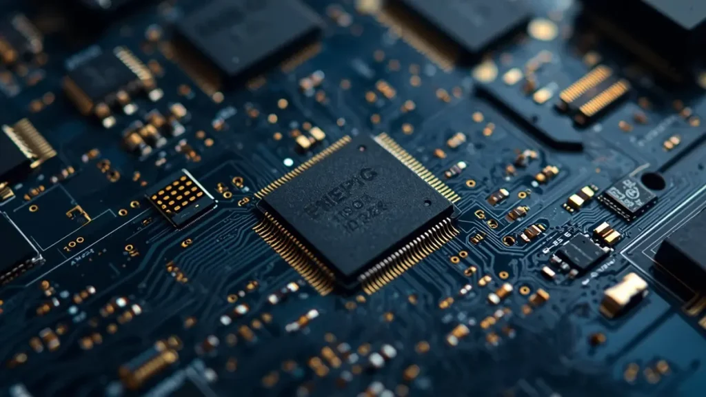
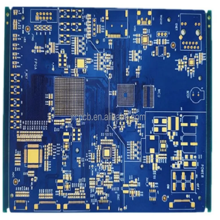
Macro inspection of a high-reliability military PCB featuring ENEPIG surface finish and protective conformal coating.
Definition and Core Identity
A military printed circuit board is a high-reliability PCB engineered, fabricated, and tested to standards far exceeding commercial or even industrial specifications. It is sometimes referred to as a ruggedized PCB or defense-grade circuit board, terms that emphasize its ability to survive hostile operational environments without functional degradation.
The defining characteristic of any military circuit board is its adherence to a zero-failure philosophy. In commercial electronics, a certain defect rate is statistically acceptable and economically optimized. In military applications—where a single board failure could disable a radar during an intercept mission, corrupt missile guidance data, or sever battlefield communications—there is no acceptable failure mode. Every military PCB must be designed, manufactured, and verified with the assumption that failure is not an option.
Key Characteristics of Military PCBs
表格
| Characteristic | Commercial PCB | Military PCB |
|---|---|---|
| Expected Lifespan | 3–5 years | 20–40 years |
| Operating Temperature | 0°C to 70°C | -55°C to +125°C (often wider) |
| Failure Tolerance | Statistically optimized (ppm level) | Zero-failure philosophy |
| Environmental Sealing | Minimal | Hermetic / conformal coated |
| Traceability | Batch-level | Unit-level, full material genealogy |
| Certification | IPC Class 2 (typical) | IPC Class 3, MIL-PRF-31032, MIL-STD-810 |
| Shock/Vibration | Minimal | MIL-STD-202G, Method 214 |
| EMI/EMC | Basic compliance | MIL-STD-461, full shielding design |
Military PCBs also demand full traceability—every laminate sheet, every copper foil roll, every chemical batch, and every process parameter must be documented and retrievable for the entire service life of the board. This is not merely a quality preference; it is a contractual and regulatory requirement under programs governed by MIL-PRF-31032 and ITAR (International Traffic in Arms Regulations).
Why Are Military PCBs Different from Commercial PCBs?
Reliability Requirements: The Orders-of-Magnitude Gap
The reliability gap between commercial and military PCBs is not incremental—it is orders of magnitude. A commercial board might be designed for 1,000 power cycles. A military circuit board for a satellite ground station must survive 50,000+ thermal cycles over two decades without impedance drift, via cracking, or solder joint fatigue.
This gap manifests in every design decision:
- Trace geometry: Military designs use wider safety margins for current density and voltage clearance
- Via structures: Stacked and filled microvias replace simple through-holes to eliminate stress concentrators
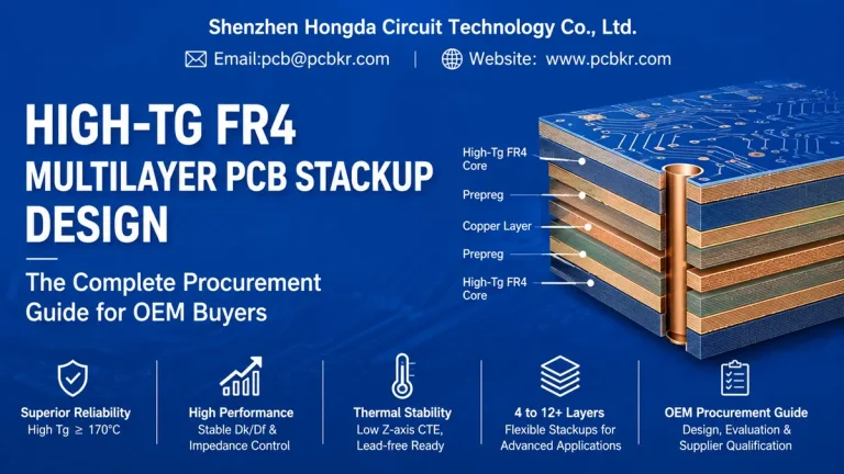
- Material selection: High-Tg FR-4 (Tg ≥ 170°C), polyimide, or ceramic substrates replace standard epoxy
- Surface finishes: Hard gold or ENEPIG replace HASL to prevent oxidation over decades
Lifecycle Expectations: Designing for a Generation
Military platforms are not replaced on consumer product cycles. A naval combat system installed in 2026 may still be operational in 2060. The PCB inside it must remain electrically stable, mechanically sound, and chemically inert across that entire span. This drives requirements for:
- Anti-tin-whisker plating to prevent latent short circuits
- Low-outgassing materials for space-adjacent applications
- UV-resistant solder mask for outdoor deployed systems
- Corrosion-resistant finishes for marine environments
Extreme Operating Conditions
Military electronics operate across the full spectrum of Earth’s harshest environments:
- Desert: Temperature swings from sub-zero nights to 70°C daytime surface temperatures, combined with abrasive sand infiltration
- Arctic: Continuous operation at -55°C with thermal shock from rapid equipment startup
- Marine: Salt spray, humidity saturation, and galvanic corrosion in naval hulls and coastal installations
- High Altitude: Reduced air pressure affecting dielectric strength and thermal convection cooling
- Space-Adjacent: Radiation exposure, vacuum outgassing, and extreme thermal cycling in near-space platforms
Each environment imposes unique material and design constraints that commercial PCB engineering simply does not address.
Mission-Critical Electronics: When Failure Is Not an Option
The term “mission-critical” is often overused in marketing. In military PCB applications, it has literal meaning. A failed board in an electronic warfare system means lost situational awareness. A failed board in missile guidance means a weapon off-target. A failed board in secure communications means compromised operational security.
This reality drives the entire military PCB ecosystem—from the IPC-6012DS specification that governs base material qualification, to the MIL-STD-810 environmental testing protocols, to the AS9100 quality management systems that military PCB manufacturers must maintain.
Military PCB Applications
Military printed circuit boards serve as the nervous system of modern defense platforms. Their applications span virtually every domain of military operations:
Radar Systems
Phased-array radar systems for air defense, naval surveillance, and ground-based early warning require high-frequency PCBs with precise impedance control and minimal signal loss. Modern AESA (Active Electronically Scanned Array) radars demand multilayer RF boards with embedded stripline structures, low-loss dielectrics, and thermal management layers to dissipate heat from thousands of transmit/receive modules.
Missile Guidance
Guidance computers in precision munitions must survive extreme acceleration (often exceeding 50g), high-G shock at intercept, and wide temperature ranges while processing sensor data in real time. These systems typically use rigid-flex PCBs to accommodate compact form factors and vibration isolation.
Electronic Warfare (EW)
EW systems—including jammers, decoys, and signals intelligence platforms—operate at frequencies from HF through millimeter-wave. Their PCBs require specialized RF materials (Rogers, PTFE-based laminates), controlled dielectric constants, and EMI shielding structures integrated into the board stack-up.
Communication Equipment
Tactical radios, satellite terminals, and battlefield networking gear demand mixed-signal PCBs with isolated analog and digital sections, secure trace routing, and conformal coating for environmental protection. Secure communication devices add requirements for tamper-evident PCB designs and anti-reverse-engineering features.
Satellite Ground Systems
Ground stations for military satellite constellations process enormous data throughput while operating in controlled environments—but the PCBs must still meet military reliability standards and often incorporate redundant signal paths for fault tolerance.
UAV Systems
Unmanned aerial vehicles represent one of the fastest-growing segments of military PCB demand. UAV flight controllers, sensor payloads, and communication links require lightweight HDI boards, often in rigid-flex configurations, that can survive launch shock, in-flight vibration, and landing impact.
Military Vehicles
Armored vehicles, tanks, and tactical trucks subject their electronics to continuous vibration, shock from rough terrain, and electromagnetic interference from high-power electrical systems. Military vehicle PCBs use heavy copper layers (6–10 oz) for power distribution and thick conformal coatings for protection.
Naval Electronics
Shipboard electronics face salt spray, humidity, and galvanic corrosion. Naval PCB assemblies require specialized conformal coatings (parylene, urethane), hermetic sealing for critical modules, and materials selected for marine corrosion resistance.
Avionics
Military aircraft avionics operate under severe constraints: weight reduction, space limitation, thermal management at altitude, and compliance with DO-160 environmental standards. Avionics PCBs frequently use rigid-flex construction to fit into compact airframe compartments while maintaining signal integrity at high data rates.
Secure Communication Devices
Encrypted radios, tactical data terminals, and cryptographic modules require PCBs with electromagnetic shielding, tamper-detection circuitry, and anti-tamper physical designs. These boards often incorporate specialized security features at the PCB layout level.
Military PCB Design Requirements
High-Speed Signal Integrity: 112G and Beyond
Modern military systems process data at rates that were unimaginable a decade ago. High-speed digital backplanes in radar and communication systems now operate at 112G PAM4 signaling, with 224G interfaces entering prototype phase for next-generation platforms.
At these speeds, signal integrity becomes a board-level physics problem:
- Insertion loss must be minimized through low-Dk/Df materials and smooth copper surfaces
- Crosstalk must be controlled through precise trace spacing and ground referencing
- Impedance tolerance must be held within ±5% (often ±2% for critical differential pairs)
- Via stubs must be eliminated through backdrilling or blind/buried via structures
Controlled Impedance and Differential Pair Routing
Military high-speed designs require rigorous impedance control. Single-ended traces typically target 50Ω ±10%, while differential pairs target 100Ω differential ±5%. Achieving this requires:
- Precise dielectric thickness control during lamination
- Laser direct imaging (LDI) for accurate trace width definition
- Real-time impedance testing using TDR (Time Domain Reflectometry)
- Coupon validation on every production panel
EMI/EMC Design
Military electromagnetic compatibility requirements under MIL-STD-461 are among the most stringent in electronics. PCB-level EMI design includes:
- Dedicated ground planes with minimal splits
- Controlled return current paths
- Stitching vias for high-frequency grounding
- Embedded shielding layers for sensitive analog circuits
- Filter components integrated at board level
Thermal Design
Power density in military electronics continues to increase. Modern radar T/R modules, power amplifiers, and processing units generate heat densities that challenge conventional cooling. Military PCB thermal design employs:
- Metal-core substrates or embedded copper coins for localized heat spreading
- Thermal vias (often filled with conductive epoxy or copper) under high-power components
- Heavy copper layers (up to 20 oz) for power distribution and heat conduction
- Thermally conductive dielectric materials
Power Integrity
Military systems often operate from noisy power sources (vehicle alternators, aircraft generators, battery banks). Power integrity design ensures stable voltage delivery to sensitive components through:
- Multi-layer power distribution networks with dedicated power and ground planes
- Embedded decoupling capacitors for high-frequency noise suppression
- Controlled plane impedance to minimize switching noise
- Isolated power domains for analog and digital sections
Shock and Vibration Resistance
Military PCBs must survive mechanical stresses that would destroy commercial boards. Design techniques include:
- Component underfill for BGA and QFN packages
- Conformal coating for mechanical reinforcement and environmental sealing
- Stiffener bars or metal brackets for large boards
- Avoidance of tall components in high-vibration zones
- Flexible PCB sections to isolate vibration in rigid-flex designs
High Layer Count Design
Modern military systems require dense interconnect that drives layer counts upward. At Shenzhen Hongda Circuit Technology, we routinely manufacture military PCBs from 4 layers up to 20+ layers, with some specialized backplane designs exceeding 30 layers. High layer count designs require:
- Sequential lamination with precise registration control
- Advanced via structures (blind, buried, stacked, staggered)
- Careful thermal management to prevent warpage during fabrication
- Rigorous impedance control across all signal layers
Military PCB Materials
Material selection is one of the most critical decisions in military PCB engineering. The substrate material determines thermal performance, mechanical stability, signal integrity, and long-term reliability.
High-Tg FR-4
High glass-transition temperature FR-4 (Tg ≥ 170°C, often 180°C+) remains the workhorse material for many military applications. It offers excellent cost-effectiveness while meeting the thermal and mechanical requirements of IPC-6012 Class 3. For military use, we specify halogen-free, low-CTE variants with enhanced CAF (Conductive Anodic Filament) resistance.
Polyimide
Polyimide substrates (Tg ~260°C) are the material of choice for extreme temperature applications, flexible and rigid-flex military PCBs, and space-qualified electronics. Polyimide offers:
- Exceptional thermal stability across -269°C to +400°C
- Excellent chemical resistance
- Low outgassing for vacuum applications
- Superior flexibility for dynamic flex applications
Rogers and High-Frequency Laminates
For radar, EW, and communication systems operating above 1 GHz, standard FR-4 introduces unacceptable signal loss. Rogers Corporation materials (RO4000 series, RO3000 series, RT/duroid) provide:
- Low dielectric constant (Dk 2.2–6.15, depending on grade)
- Low dissipation factor (Df as low as 0.0009)
- Stable electrical properties across temperature and frequency
- Excellent thermal conductivity for heat dissipation
PTFE-Based Materials
Polytetrafluoroethylene (PTFE) based laminates offer the lowest dielectric loss available in commercial PCB materials. They are essential for millimeter-wave radar, satellite communication, and EW systems where every decibel of signal loss matters. PTFE materials require specialized fabrication processes but deliver unmatched RF performance.
Ceramic PCB
Ceramic substrates (alumina, aluminum nitride, beryllium oxide) provide the ultimate combination of thermal conductivity and electrical insulation. They are used in high-power RF amplifiers, power modules, and applications where thermal management is the dominant design constraint. Ceramic PCBs require specialized manufacturing but offer thermal conductivity up to 170 W/m·K (aluminum nitride).
Heavy Copper PCB
Military power distribution boards, motor controllers, and high-current systems require copper weights far exceeding standard 1 oz (35 μm). Heavy copper PCBs use 6 oz, 10 oz, or even 20 oz copper layers to:
- Carry high current with minimal temperature rise
- Provide structural rigidity for large boards
- Act as heat spreaders for power components
- Survive thermal cycling without trace cracking
At Shenzhen Hongda Circuit Technology, our heavy copper process achieves aspect ratios up to 20:1 in through-hole plating, ensuring reliable connections even in the thickest boards.
Low-Loss Laminates: Megtron 6, Megtron 7, Isola Tachyon
For 112G+ signaling and high-frequency RF applications, next-generation low-loss materials have become essential:
- Megtron 6 (Panasonic): Dk 3.7, Df 0.002, Tg 185°C—ideal for high-speed digital backplanes
- Megtron 7 (Panasonic): Dk 3.3, Df 0.001, Tg 200°C—next-generation material for 224G signaling
- Isola Tachyon: Dk 3.0, Df 0.0017, Tg 200°C—optimized for high-speed computing and AI hardware
These materials, combined with HVLP (very low profile) copper foil, enable signal transmission at speeds exceeding 224 Gbps with minimal attenuation.
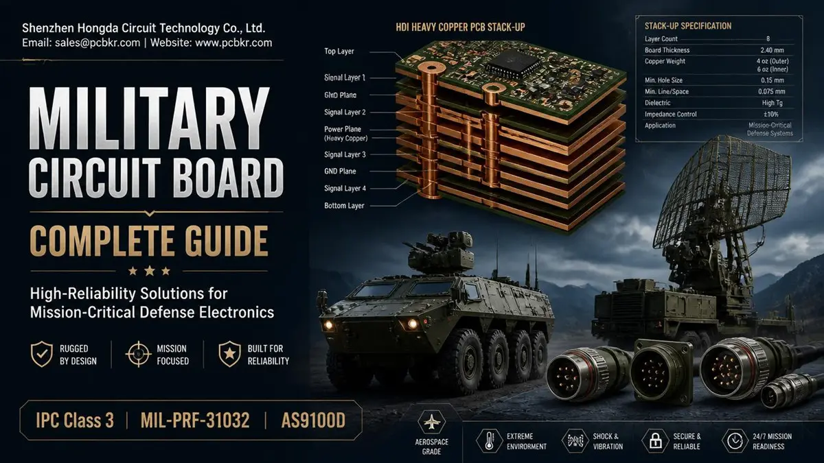
Military PCB Stack-Up Design
Typical Layer Structures
Military PCB stack-ups are designed for electrical performance, mechanical stability, and manufacturability. Common configurations include:
表格
| Layer Count | Typical Application | Key Features |
|---|---|---|
| 4 Layers | Simple control boards, power supplies | Signal-Ground-Power-Signal |
| 6 Layers | Moderate complexity, mixed signal | Dedicated ground and power planes, signal routing on outer layers |
| 8 Layers | High-speed digital, moderate RF | Multiple ground planes, controlled impedance layers, power distribution |
| 12 Layers | Complex digital, radar processing | Sequential lamination, blind/buried vias, embedded passives |
| 20+ Layers | Backplanes, high-density computing | Any-layer HDI, microvia structures, advanced thermal management |
Power Plane Design
Military PCB power distribution requires careful plane design to minimize noise and ensure stable voltage delivery. Best practices include:
- Solid power planes (no splits under high-speed signals)
- Adequate plane capacitance between power and ground pairs
- Multiple decoupling capacitor values distributed across the board
- Ferrite beads and filters at power entry points
Ground Shielding
Proper ground design is essential for both signal integrity and EMI compliance:
- Continuous ground planes with minimal interruptions
- Ground vias stitching around high-speed traces and RF structures
- Separate analog and digital ground domains with single-point connection
- Guard rings around sensitive analog circuits
High-Speed Routing
High-speed signal routing in military PCBs follows strict rules:
- Differential pairs with matched length (within 5 mils)
- Controlled trace spacing to maintain impedance
- Avoidance of plane splits and via stubs
- Serpentine routing for length matching, minimizing coupling
- Proper termination at source and/or load
Military PCB Manufacturing Process
The manufacturing of a military-grade printed circuit board involves processes that are significantly more rigorous than commercial fabrication. At Shenzhen Hongda Circuit Technology, we have invested in advanced equipment and refined processes specifically for defense-grade production.
Material Preparation and Incoming Inspection
Every military PCB begins with verified materials. Our incoming inspection process includes:
- Certificate of conformance verification for all laminates
- Tg testing via DSC (Differential Scanning Calorimetry)
- Copper foil thickness measurement
- Dielectric constant verification for RF materials
- Moisture content testing for hygroscopic materials
Laser Direct Imaging (LDI)

High-precision Laser Direct Imaging (LDI) technology ensures fine trace accuracy and tight impedance control for military-grade PCBs.
Traditional photolithography uses photographic masks that introduce alignment errors and resolution limitations. Our Laser Direct Imaging (LDI) systems expose circuit patterns directly onto photoresist-coated panels using high-precision UV lasers.
LDI advantages for military PCBs:
- Resolution: Achieves line widths down to 15–40 μm with mSAP process, critical for HDI military boards
- Registration accuracy: Interlayer alignment within ±25 μm, essential for multilayer registration
- Flexibility: No mask tooling required, enabling rapid design changes for prototype military programs
- Consistency: Eliminates mask wear and variation, ensuring every panel matches the design database exactly
The LDI market is projected to grow from USD 800 million in 2025 to USD 1.345 billion by 2032, reflecting the industry’s shift toward maskless imaging for high-density applications.
Automated Optical Inspection (AOI)
Our production lines incorporate 3D AOI systems with AI-powered defect classification. Unlike 2D AOI that analyzes flat images, 3D AOI captures full topographic data—height, volume, coplanarity, and warpage—reducing false-call rates by 60–80% compared to legacy systems.
For military PCBs, where defect escape is unacceptable, our AOI process includes:
- 100% panel inspection at multiple production stages
- AI-trained deep learning models for defect recognition
- Real-time SPC (Statistical Process Control) integration
- Defect categorization and automatic routing for review
Laser Drilling
Microvia formation in military HDI boards requires precision that mechanical drilling cannot achieve. Our UV laser drilling systems create blind vias as small as 50 μm in diameter with smooth hole walls free of glass fiber burrs. This is essential for:
- High-density BGA fanout (0.4 mm pitch and below)
- Stacked via structures for layer transitions
- RF applications where via wall quality affects signal integrity
Via Filling
Unfilled vias create structural weak points and thermal stress concentrators. Our vacuum-assisted via filling process uses conductive copper paste to completely fill microvias, creating:
- Flat surfaces for component mounting (via-in-pad)
- Enhanced thermal conductivity through the via barrel
- Improved mechanical strength under thermal cycling
- Reliable interlayer connections in stacked via structures
Sequential Lamination
High layer count military PCBs require sequential lamination—building the board in stages, drilling and plating vias between stages. This enables:
- Buried via structures for dense routing
- Stacked microvias for HDI interconnect
- Controlled impedance across all signal layers
- Registration accuracy maintained through optical alignment systems
Our vacuum lamination presses eliminate air gaps between layers, ensuring boards pass 20+ thermal shock cycles without delamination—a critical requirement for military environmental testing.
mSAP (Modified Semi-Additive Process)
For ultra-fine line military PCBs, we employ mSAP technology—the standard production route for 2026 high-performance communication and defense electronics. Unlike traditional subtractive etching that etches away from thick copper foil, mSAP builds traces up from a thin seed layer.
mSAP advantages:
- Line width/spacing: 15–40 μm, enabling 3× the routing density of conventional processes
- Impedance control: ±2% tolerance, critical for 112G/224G signaling
- Edge definition: Near-vertical trace sidewalls with minimal undercut
- Yield: Higher first-pass yield on ultra-fine line designs
A full mSAP production line represents a capital investment exceeding 80 million RMB, reflecting the advanced capability required for next-generation military electronics.
Copper Plating
Our pulse plating systems deliver uniform copper deposition across the entire panel, including high-aspect-ratio through-holes and microvias. For military applications, we achieve:
- Through-hole aspect ratios up to 20:1
- Microvia plating with 25 μm minimum hole diameter
- Copper thickness uniformity within ±10%
- Void-free plating verified by X-ray inspection
Surface Finish
Surface finish selection for military PCBs balances solderability, shelf life, and environmental resistance:
表格
| Finish | Shelf Life | Solderability | Wire Bonding | Cost | Best For |
|---|---|---|---|---|---|
| ENIG | 12+ months | Excellent | Good | Medium | General military, BGA assemblies |
| ENEPIG | 24+ months | Excellent | Excellent | High | High-reliability, gold wire bonding |
| Immersion Silver | 6–12 months | Excellent | Poor | Low | Short-lead military prototypes |
| Hard Gold | 24+ months | Good | Excellent | High | Edge connectors, wear surfaces |
For most military applications, ENIG (Electroless Nickel Immersion Gold) provides the optimal balance of corrosion resistance, solderability, and shelf life. For applications requiring wire bonding or extreme long-term storage, ENEPIG (Electroless Nickel Electroless Palladium Immersion Gold) is specified.
Final Inspection
Every military PCB undergoes comprehensive final inspection before release:
- 100% electrical testing (flying probe or ICT)
- Impedance coupon measurement and documentation
- Cross-sectional analysis for via quality verification
- Solderability testing per IPC-J-STD-003
- Visual inspection per IPC-A-610 Class 3 criteria
- Dimensional verification against design database
Military PCB Manufacturing Capabilities at Shenzhen Hongda Circuit Technology
Maximum Layers: Up to 30+ Layers
Our facility is equipped to manufacture military PCBs from simple 2-layer designs up to complex 30+ layer backplanes. High layer count capability is essential for:
- Radar signal processing backplanes
- Satellite communication routing matrices
- Military computing server motherboards
- Multi-domain power distribution systems
HDI Technology: Any-Layer Interconnect
Our HDI manufacturing supports up to 7-level HDI with any-layer interconnect, enabling:
- BGA pitch down to 0.3 mm
- Laser microvias at 75 μm diameter
- Stacked and staggered via structures
- 25 μm trace/space capability with mSAP
Blind and Buried Vias
Blind vias (connecting outer to inner layers) and buried vias (connecting internal layers only) enable dense routing without consuming surface area. Our capabilities include:
- Blind vias: 50–150 μm diameter, laser drilled
- Buried vias: 100–200 μm diameter, mechanically drilled
- Stacked vias: Multiple microvias stacked vertically for layer transitions
- Staggered vias: Offset microvias for improved reliability
Via-in-Pad Technology
Via-in-pad places microvias directly under component pads, enabling maximum component density. This is critical for:
- Fine-pitch BGA packages (0.4 mm and below)
- Miniaturized UAV electronics
- Wearable military devices
- Compact communication modules
Our vacuum via filling process ensures flat, reliable via-in-pad structures suitable for direct component mounting.
mSAP and Advanced Etching
Our mSAP line enables ultra-fine trace production for next-generation military electronics:
- Line width/spacing: 15–40 μm
- Impedance tolerance: ±2%
- Layer registration: ±25 μm
- Applications: 112G/224G backplanes, RF front-ends, AI processing modules
Heavy Copper: Up to 20 oz
For high-power military applications, our heavy copper process supports:
- Copper weights: 6 oz, 10 oz, 15 oz, 20 oz+
- Embedded copper coins for localized heat spreading
- Through-hole aspect ratio: 20:1
- Applications: Power distribution, motor drives, radar T/R modules
Rigid-Flex and Flex PCB
Military systems increasingly require rigid-flex PCBs to fit into compact, irregular spaces while maintaining electrical connectivity across moving or hinged sections. Our capabilities include:
- Rigid-flex structures up to 20 layers
- Dynamic flex cycles: 10,000+ bends
- Polyimide flex layers for extreme temperature
- Controlled impedance across rigid and flex sections
Backdrilling
For high-speed military PCBs, via stubs create unwanted resonances and signal reflections. Our backdrilling process removes unused via barrel sections:
- Stub removal down to 8 mil (0.2 mm) residual
- Controlled depth drilling with ±2 mil accuracy
- Improves signal integrity for 10G+ designs
- Reduces crosstalk in dense backplanes
Military PCB Assembly
SMT Assembly
Our SMT lines are qualified for military-grade assembly with:
- Component placement accuracy: ±25 μm
- Capability for 01005 components and 0.3 mm pitch BGAs
- Nitrogen reflow for improved solder joint quality
- X-ray inspection for BGA and QFN solder joints
Through-Hole Assembly
For military connectors, power components, and legacy designs, our through-hole assembly includes:
- Wave soldering with nitrogen atmosphere
- Selective soldering for mixed-technology boards
- Robotic soldering for precision applications
- 100% solder joint inspection per IPC-A-610 Class 3
Selective Soldering
Selective soldering enables precise through-hole component attachment without affecting nearby SMT components. This is essential for:
- Mixed-technology military boards
- High-thermal-mass connectors
- Components requiring specific solder profiles
Conformal Coating
Military PCBs require conformal coating for environmental protection. We offer:
- Acrylic: Easy repair, good moisture resistance
- Urethane: Excellent chemical resistance, abrasion resistant
- Silicone: Extreme temperature range, flexible
- Parylene: Ultimate protection, pinhole-free, medical/space grade
Coating thickness is controlled to 25–75 μm per IPC-CC-830 requirements, with 100% UV inspection for coverage verification.
Underfill
For BGA and chip-scale packages in high-vibration military environments, underfill provides:
- Mechanical reinforcement of solder joints
- Stress distribution under thermal cycling
- Improved board-level reliability
- Compliance with MIL-STD-202 shock/vibration requirements
Box Build
Our box build capabilities extend from PCB assembly to complete system integration:
- Cable harness fabrication and testing
- Mechanical assembly and integration
- System-level functional testing
- Environmental stress screening
- Final packaging and documentation
Military PCB Testing
Testing is where military PCBs prove their reliability. Our testing protocols exceed commercial standards and align with MIL-specification requirements.
Flying Probe Testing
For prototype and low-volume military PCBs, flying probe testing provides:
- 100% electrical connectivity verification
- Component value measurement (resistors, capacitors)
- Diode and transistor junction testing
- No fixture required, enabling rapid prototype turnaround
In-Circuit Testing (ICT)
For volume production, ICT fixtures provide:
- Comprehensive electrical verification
- Component orientation and value checking
- Short and open circuit detection
- High-voltage isolation testing
Functional Testing
Functional testing validates that the assembled PCB performs its intended function:
- Custom test fixture design
- Boundary scan (JTAG) testing for complex digital boards
- RF performance verification for communication boards
- Power consumption and thermal profiling
AOI (Automated Optical Inspection)
Post-assembly AOI verifies:
- Component presence and orientation
- Solder joint quality (bridging, insufficient solder, tombstones)
- Component placement accuracy
- Conformal coating coverage
Our 3D AOI systems with AI classification reduce false calls while ensuring zero defect escape.
X-Ray Inspection
X-ray inspection reveals hidden defects invisible to optical methods:
- BGA solder ball void analysis
- QFN thermal pad solder coverage
- Through-hole barrel fill verification
- Internal via and laminate defect detection
For military applications, we use 3D CT X-ray for comprehensive volumetric analysis of critical solder joints.
Thermal Cycling
Thermal cycling tests simulate the temperature extremes of military operation:
- Test range: typically -55°C to +125°C
- Cycle count: 500–1,000 cycles for qualification
- Monitoring: electrical continuity and impedance during cycling
- Acceptance: zero failures, minimal resistance drift
Salt Spray Testing
For marine and coastal military applications, salt spray testing per ASTM B117 validates:
- Surface finish corrosion resistance
- Conformal coating integrity
- Solder joint protection
- Duration: typically 96–500 hours
Vibration Testing
Vibration testing per MIL-STD-202G, Method 204 simulates operational vibration:
- Random vibration: 5–2,000 Hz, 7.7g RMS
- Sinusoidal vibration: 10–2,000 Hz, 20g peak
- Duration: typically 4 hours per axis
- Monitoring: electrical continuity during vibration
Shock Testing
Shock testing per MIL-STD-202G, Method 213 validates survival of high-G events:
- Half-sine shock: 50g, 11 ms duration
- Sawtooth shock: 30g, 11 ms duration
- Monitoring: electrical continuity and functional verification post-shock
Burn-In Testing
Burn-in testing accelerates early-life failures through extended operation at elevated temperature:
- Temperature: typically +85°C to +125°C
- Duration: 168–500 hours
- Electrical loading: full operational stress
- Objective: eliminate infant mortality failures before field deployment
Thermal Vacuum Testing
For space-adjacent military applications, thermal vacuum testing simulates the space environment:
- Vacuum level: < 10⁻⁵ Torr
- Temperature cycling: -55°C to +125°C
- Outgassing measurement per ASTM E595
- Duration: mission-profile simulation
Military PCB Standards and Certifications
Military PCB manufacturing operates within a rigorous framework of standards that govern every aspect of design, fabrication, assembly, and testing.
IPC Class 3
IPC Class 3 is the highest reliability classification for printed circuit boards. It requires:
- Continuous high performance with no equipment downtime tolerance
- Strict adherence to design, material, and process requirements
- Enhanced plating thickness and annular ring requirements
- 100% electrical testing
- Detailed process control and documentation
All military PCBs manufactured at Shenzhen Hongda Circuit Technology meet or exceed IPC Class 3 requirements.
IPC-6012DS
IPC-6012DS is the qualification and performance specification for rigid printed boards in military and aerospace applications. It defines:
- Base material requirements and qualification
- Conductor definition and spacing
- Hole wall quality and plating thickness
- Solderability and cleanliness requirements
- Environmental testing protocols
IPC-A-610 Class 3
IPC-A-610 Class 3 defines the acceptability criteria for electronic assemblies in high-performance applications. It covers:
- Component mounting and orientation
- Solder joint quality (through-hole and SMT)
- Cleanliness and contamination limits
- Conformal coating requirements
- Hardware installation criteria
MIL-PRF-31032
MIL-PRF-31032 is the U.S. Department of Defense performance specification for printed circuit boards. It is the gold standard for military PCB qualification and requires:
- Approved base material systems
- Verified manufacturing processes
- Comprehensive testing and inspection protocols
- Full traceability and documentation
- Periodic requalification audits
Manufacturers qualified to MIL-PRF-31032 are listed on the Defense Logistics Agency’s Qualified Products List (QPL), making them eligible for direct military procurement.
MIL-STD-810
MIL-STD-810 defines environmental engineering considerations and laboratory tests for military equipment. Relevant test methods for PCBs include:
- Method 501: High temperature
- Method 502: Low temperature
- Method 507: Humidity
- Method 509: Salt spray
- Method 514: Vibration
- Method 516: Shock
- Method 520: Temperature, humidity, vibration, altitude
MIL-STD-461
MIL-STD-461 defines electromagnetic compatibility requirements for military equipment. PCB-level compliance requires:
- Controlled impedance design
- Proper grounding and shielding
- Filtered power entry points
- EMI gasket integration at enclosure interfaces
MIL-STD-202
MIL-STD-202 establishes test methods for electronic and electrical component parts. Key methods for PCBs include:
- Method 106: Moisture resistance
- Method 107: Thermal shock
- Method 108: Life testing
- Method 204: Vibration
- Method 213: Shock
- Method 215: Solvent resistance
AS9100
AS9100 is the aerospace quality management standard based on ISO 9001 with additional requirements for aviation, space, and defense. It covers:
- Configuration management
- Risk management
- Special requirements for critical items
- Supplier monitoring and control
- First article inspection
ISO 9001
ISO 9001 is the foundation of our quality management system, ensuring:
- Customer-focused processes
- Continuous improvement
- Documented procedures and records
- Management review and internal audits
ITAR Considerations
The International Traffic in Arms Regulations (ITAR) governs the export of defense-related articles and technical data. For military PCB manufacturers, ITAR compliance requires:
- Controlled access to technical data
- Secure facility and IT infrastructure
- Trained personnel with security clearances
- Proper licensing for international shipments
- End-use verification for all defense-related products
Military PCB Quality Control
Incoming Inspection
Every material entering our facility undergoes rigorous incoming inspection:
- Certificate of conformance verification
- Dimensional and thickness measurement
- Electrical property verification (Dk, Df for RF materials)
- Visual inspection for defects and contamination
- Moisture content testing for hygroscopic materials
Process Control
Our manufacturing processes are controlled through:
- SPC (Statistical Process Control) charts for critical parameters
- Automated process monitoring with alarm thresholds
- Preventive maintenance schedules for all equipment
- Change control procedures for process modifications
AOI at Multiple Stages
AOI is performed at critical process checkpoints:
- Post-etch: Trace width, spacing, and defect detection
- Post-drilling: Hole quality and positioning verification
- Post-plating: Copper thickness uniformity
- Post-solder mask: Registration and coverage verification
- Post-assembly: Component placement and solder joint quality
X-Ray Inspection
X-ray inspection provides non-destructive verification of:
- Internal via fill quality
- BGA solder ball integrity
- Hidden solder joint defects
- Laminate delamination
- Embedded component placement
Cross-Section Analysis
Cross-sectional analysis (microsectioning) is performed on sample coupons to verify:
- Copper plating thickness (barrel and surface)
- Via fill quality and void content
- Layer-to-layer registration
- Dielectric thickness uniformity
- Solder mask thickness and adhesion
Microsection
Microsection examination at 100×–1,000× magnification validates:
- Intermetallic compound formation at solder joints
- Copper grain structure
- Laminate integrity
- Plating adhesion
- Etch quality and edge definition
Solderability Testing
Solderability testing per IPC-J-STD-003 verifies that surface finishes provide reliable wetting:
- Dip-and-look testing
- Wetting balance measurement
- Surface insulation resistance testing
- Aging simulation for shelf-life validation
Reliability Database
We maintain a comprehensive reliability database that tracks:
- All test results by part number and production lot
- Failure analysis reports and corrective actions
- Supplier performance metrics
- Customer field performance data
- Continuous improvement initiatives
Military PCB vs Aerospace PCB
While military and aerospace PCBs share many requirements, there are important distinctions:
表格
| Parameter | Military PCB | Aerospace PCB |
|---|---|---|
| Primary Standards | MIL-PRF-31032, MIL-STD-810 | AS9100, IPC-6012DS, NASA-STD-8739 |
| Temperature Range | -55°C to +125°C (typical) | -65°C to +150°C (often wider) |
| Radiation Hardness | Limited (space-adjacent only) | Often required (space applications) |
| Outgassing | Moderate concern | Critical (vacuum environments) |
| Weight Sensitivity | Moderate | Extreme (launch cost per kg) |
| Cost Tolerance | Higher (defense budgets) | Very high (space qualification) |
| Application Focus | Ground, sea, air combat systems | Satellites, launch vehicles, aircraft |
| Typical Lifecycle | 20–40 years | 15–25 years (space) |
Both domains demand IPC Class 3 reliability, but aerospace adds requirements for extreme radiation tolerance, ultra-low outgassing, and weight minimization that go beyond typical military specifications.
Military PCB vs Industrial PCB
表格
| Parameter | Industrial PCB | Military PCB |
|---|---|---|
| Operating Temperature | -20°C to +85°C | -55°C to +125°C |
| Humidity Resistance | Moderate | Severe (salt spray, condensation) |
| Vibration/Shock | Moderate | Extreme (MIL-STD-202) |
| Expected Lifespan | 5–10 years | 20–40 years |
| Failure Tolerance | Low ppm | Zero-failure philosophy |
| Traceability | Batch-level | Unit-level with full genealogy |
| Certification | IPC Class 2 (typical) | IPC Class 3, MIL-PRF-31032 |
| Cost | Lower | Higher (2–5×) |
Industrial PCBs are designed for factory automation, process control, and heavy equipment. They offer good reliability at moderate cost but lack the extreme environmental tolerance and traceability required for defense applications.
Military PCB Cost Factors
Military PCB costs are higher than commercial equivalents due to the cumulative effect of multiple factors:
Layer Count
Each additional layer increases material cost, processing time, and yield risk. A 20-layer military PCB can cost 5–10× more than a 4-layer commercial board of the same dimensions.
Material Selection
Specialized materials significantly impact cost:
- Standard FR-4: Baseline cost
- High-Tg FR-4: +20–30%
- Polyimide: +50–100%
- Rogers/PTFE: +100–300%
- Ceramic: +200–500%
- Low-loss laminates (Megtron 6/7): +80–150%
HDI Complexity
HDI technology adds cost through additional process steps:
- Laser drilling: +15–25%
- Sequential lamination: +20–40% per additional lamination cycle
- Via filling: +10–20%
- mSAP processing: +30–50%
Testing Requirements
Military testing protocols add significant cost:
- 100% electrical testing: +5–10%
- Environmental testing (thermal cycling, vibration, shock): +15–30%
- X-ray inspection: +5–10%
- Cross-sectional analysis: +3–5%
Certification and Documentation
Military certification requirements add overhead:
- MIL-PRF-31032 qualification: Significant one-time investment
- AS9100/ISO 9001 maintenance: Ongoing audit and documentation costs
- ITAR compliance: Facility and personnel security investments
- Full traceability documentation: Labor and system costs
Assembly Complexity
Military assembly adds cost through:
- Conformal coating: +10–20%
- Underfill: +5–10%
- Selective soldering: +10–15%
- Box build integration: Variable
Volume
Like all manufacturing, military PCBs benefit from volume economies—but the effect is moderated by the low-volume, high-mix nature of defense programs. Prototype quantities (1–10 units) may cost 10× more per unit than production volumes (1,000+ units).
How to Choose a Military PCB Manufacturer
Selecting a military PCB supplier is one of the most consequential decisions in a defense program. The wrong choice can result in schedule delays, cost overruns, and—most critically—field failures.
Manufacturing Experience
Look for a manufacturer with:
- Documented military/aerospace program history: Request case studies and customer references
- Multi-year track record: Military programs span decades; your supplier must be stable
- Diverse application experience: Radar, communication, avionics, and ground systems each have unique requirements
- Failure analysis capability: The ability to investigate and resolve field failures
Military Certifications
Verify that your supplier maintains:
- IPC-6012DS qualification: The base standard for military PCB performance
- MIL-PRF-31032 QPL listing: Required for direct U.S. defense procurement
- AS9100 certification: Aerospace quality management standard
- ISO 9001 certification: Foundation quality management system
- ITAR registration: Required for U.S. defense technical data
Engineering Support
Military PCB programs require close collaboration between OEM engineers and manufacturer engineering teams. Evaluate:
- DFM capability: Can they review your design and identify manufacturability issues before fabrication?
- Stack-up design support: Do they provide impedance modeling and material recommendations?
- Signal integrity consulting: Can they advise on high-speed routing and via structures?
- Prototyping flexibility: Can they support rapid iteration for development programs?
Advanced Equipment
Modern military PCBs require advanced manufacturing equipment:
- LDI systems: For fine-line imaging and rapid prototyping
- Laser drilling: For microvia formation in HDI boards
- mSAP lines: For ultra-fine trace production
- 3D AOI with AI: For defect detection without false-call fatigue
- X-ray inspection: For hidden defect verification
- Environmental testing chambers: For thermal cycling and humidity testing
Supply Chain Security
Defense supply chains are under increasing scrutiny. Your supplier should demonstrate:
- Material traceability: Full genealogy from raw material to finished board
- Supplier qualification: Approved vendor lists with periodic audits
- Inventory management: Secure storage for long-lead military materials
- Counterfeit prevention: Component authentication and testing protocols
Quality System
A robust quality system is non-negotiable:
- Documented procedures: Every process step defined and controlled
- SPC implementation: Statistical monitoring of critical parameters
- Internal audit program: Regular self-assessment and improvement
- Management review: Executive oversight of quality performance
- Corrective action system: Structured response to defects and failures
Delivery Capability
Military programs often have unforgiving schedules. Evaluate:
- Prototype lead times: Can they deliver first articles in 2–4 weeks?
- Production capacity: Can they scale from prototype to volume without quality degradation?
- On-time delivery performance: Request historical data
- Schedule risk management: How do they handle material shortages or equipment issues?
Traceability
Full traceability is a contractual requirement for most military programs:
- Unit serialization: Every board has a unique identifier
- Material lot tracking: Every material used is documented
- Process parameter logging: Every process step is recorded
- Test data retention: All test results archived for the program lifecycle
- Digital thread: Integration with customer PLM/ERP systems
Why Choose Shenzhen Hongda Circuit Technology Co., Ltd.
Shenzhen Hongda Circuit Technology Co., Ltd. has invested strategically in the equipment, processes, and personnel required to deliver military-grade printed circuit boards that meet the most demanding defense program requirements.
20+ Layer Manufacturing Capability
Our facility is equipped for high layer count production up to 30+ layers, with sequential lamination, advanced registration systems, and vacuum lamination presses that eliminate interlayer voids. This capability supports the dense backplanes and complex multilayer structures required by modern radar, communication, and computing systems.
Advanced HDI and Any-Layer Interconnect
Our HDI manufacturing line supports 7-level HDI with any-layer interconnect, laser microvias down to 75 μm, and stacked via structures. Combined with our mSAP capability for 15–40 μm trace/space, we enable the miniaturization and density required by next-generation military electronics.
Rigid-Flex and Flex PCB Expertise
We manufacture rigid-flex PCBs up to 20 layers with polyimide flex sections rated for 10,000+ dynamic flex cycles. This capability is essential for UAV systems, wearable military devices, and avionics applications where space constraints and mechanical flexibility converge.
High-Reliability Manufacturing Process
Our manufacturing process is built around the zero-failure philosophy:
- Incoming material verification: Every laminate, copper foil, and chemical batch is tested before use
- SPC-controlled processes: Critical parameters monitored in real time with automatic alarm thresholds
- Multi-stage AOI: 3D AOI with AI classification at etch, assembly, and final inspection stages
- 100% electrical testing: Every board verified for continuity, isolation, and impedance
- Environmental testing: In-house thermal cycling, vibration, and shock testing capabilities
Advanced Inspection Equipment
Our inspection infrastructure includes:
- 3D AOI systems: AI-powered defect classification with 60–80% false-call reduction
- 3D X-ray CT: Volumetric analysis of hidden solder joints and internal structures
- Flying probe testers: 100% electrical verification without fixture cost
- ICT fixtures: High-volume production testing with comprehensive coverage
- TDR impedance measurement: Real-time impedance verification for high-speed designs
Laser Drilling and Direct Imaging
Our manufacturing floor features:
- UV laser drilling systems: 50 μm minimum via diameter with smooth hole walls
- LDI (Laser Direct Imaging): Maskless imaging for rapid prototyping and precise registration
- mSAP production line: Ultra-fine trace capability for next-generation designs
- Vacuum lamination presses: Void-free multilayer construction
Controlled Impedance Expertise
We provide comprehensive impedance control services:
- Pre-manufacturing stack-up modeling and simulation
- Real-time impedance measurement using TDR
- Coupon validation on every production panel
- ±5% impedance tolerance (±2% available for critical applications)
Fast Prototype and Mass Production
We support the full product lifecycle:
- Prototype: 2–4 week turnaround for first articles
- Pre-production: Process validation and qualification builds
- Mass production: Scalable capacity with consistent quality
- Lifecycle support: Long-term availability for 20+ year programs
Global Export Experience
With extensive experience exporting to North America, Europe, and Asia-Pacific defense markets, we understand:
- International shipping documentation and customs requirements
- ITAR compliance for U.S. defense programs
- AS9100 and IPC standard alignment across regions
- Time zone coordination for program management
Frequently Asked Questions (FAQ)
What is a Military PCB?
A military PCB is a high-reliability printed circuit board engineered to survive extreme environmental conditions, operate for 20–40 years, and maintain zero-failure performance in mission-critical defense applications. It is manufactured to IPC Class 3, MIL-PRF-31032, and MIL-STD-810 standards with full material traceability.
What standards apply to military PCBs?
Key standards include IPC Class 3, IPC-6012DS, IPC-A-610 Class 3, MIL-PRF-31032, MIL-STD-810, MIL-STD-461, MIL-STD-202, AS9100, and ISO 9001. ITAR compliance is required for U.S. defense programs.
What is the difference between military and aerospace PCBs?
Military PCBs focus on ground, sea, and air combat systems with emphasis on shock, vibration, and environmental resistance. Aerospace PCBs add requirements for radiation hardness, ultra-low outgassing, and extreme weight minimization for space applications.
How much does a military PCB cost?
Military PCB costs vary widely based on layer count, material, HDI complexity, testing requirements, and volume. A simple 4-layer military PCB might cost $50–200, while a complex 20+ layer HDI board with full environmental testing could cost $1,000–5,000+ per unit in prototype quantities.
How does AI improve military PCB quality control?
AI-powered 3D AOI systems use deep learning to classify defects with 60–80% lower false-call rates than traditional rule-based systems. This reduces manual inspection burden while ensuring zero defect escape in high-reliability military production.
Request a Military PCB Quote
Shenzhen Hongda Circuit Technology Co., Ltd. provides comprehensive military PCB manufacturing services from design review through global delivery.
Our Process
- Upload Gerber Files: Submit your design files through our secure portal
- PCB Specification Review: Our engineering team reviews your stack-up, materials, and performance requirements
- Stack-up Review: We provide impedance modeling and material recommendations optimized for your application
- DFM Analysis: Our DFM engineers identify potential manufacturability issues before fabrication begins
- PCB Manufacturing: Production on our advanced equipment with full process control and inspection
- PCB Assembly: SMT, through-hole, selective soldering, conformal coating, and underfill as required
- Reliability Testing: Thermal cycling, vibration, shock, salt spray, and electrical verification
- Global Shipping: Secure packaging with full documentation and traceability records
Contact Us
For military PCB inquiries, technical consultations, or quotation requests, contact Shenzhen Hongda Circuit Technology Co., Ltd. Our engineering team is ready to support your defense program with the reliability, quality, and traceability that mission-critical applications demand.
Shenzhen Hongda Circuit Technology Co., Ltd. — Precision Manufacturing for Mission-Critical Defense Electronics
About Author
David Chen https://www.linkedin.com/in/pcbcoming
David Chen boasts an extensive professional background in PCBA manufacturing, PCBA testing, and PCBA optimization, with specialized expertise in high-precision PCBA fault analysis and rigorous PCBA reliability testing. The author has worked with high-layer-count server PCB fabrication, ultra-low-loss backplane stackups, and thermo-mechanical reliability optimization for AI infrastructure projects involving 112G and 224G PAM4 architectures. Skilled in complex circuit design and cutting-edge advanced PCB manufacturing processes, he delivers solutions that elevate product durability and performance across industrial applications. His technical articles focusing on PCBA manufacturing workflows and testing methodologies are widely cited by industry peers, research institutions, and technical platforms, solidifying his reputation as a recognized technical authority in the global circuit board manufacturing sector.