Polyimide PCB Manufacturing: Technology Trends, Supplier Selection, and a Smarter Procurement Guide
A polyimide PCB is not merely a flexible alternative to FR-4. It is a material system chosen when thermal endurance, dimensional stability, and mechanical resilience determine whether a product survives its intended lifecycle. For procurement teams, however, the challenge is rarely the material itself. The challenge is identifying which supplier can actually control that material through laser drilling, sequential lamination, impedance verification, and reliability testing—without introducing the defects that only appear after six months in the field.
This guide is written for engineering buyers, quality managers, and supply-chain directors who need more than a product brochure. It maps the 2026 technology landscape for polyimide PCB manufacturing, explains the four-stage procurement decision chain, and shows what verifiable capability looks like at Shenzhen Hongda Circuit Technology Co., Ltd.
What Is a Polyimide PCB and Why Procurement Teams Need a Structured Selection Process
A polyimide PCB uses polyimide film—most commonly Kapton-grade or equivalent high-performance formulations—as the dielectric substrate. Unlike standard glass-reinforced epoxy, polyimide maintains mechanical and electrical integrity across temperature ranges from –269 °C to over 400 °C, depending on the resin system. This makes it the default choice for flexible printed circuit boards, rigid-flex PCBs, and certain high-temperature rigid multilayer boards where FR-4 would degrade.
The material landscape has expanded beyond basic adhesive-based constructions. In 2026, buyers routinely specify:
- Adhesive-free polyimide copper-clad laminates for thinner, more dimensionally stable flex circuits
- Filled and low-flow polyimide formulations for aerospace and automotive thermal cycling
- Hybrid stack-ups combining polyimide flex layers with high-Tg rigid cores for rigid-flex HDI designs
- Low-loss polyimide and LCP blends for millimeter-wave and high-frequency RF channels
The procurement mistake most teams make is treating “polyimide PCB supplier” as a generic category. In reality, a fabricator qualified for 2-layer static flex circuits may lack the laser drilling precision, coverlay registration control, or impedance verification systems needed for a 16-layer rigid-flex board with stacked microvias. The selection process must therefore be staged, evidence-based, and focused on controlled outcomes rather than marketing claims.
Polyimide PCB Manufacturing Technology Trends Shaping Supplier Capability
Adhesive-Free Polyimide PCB Construction for High-Reliability Flexible Circuits
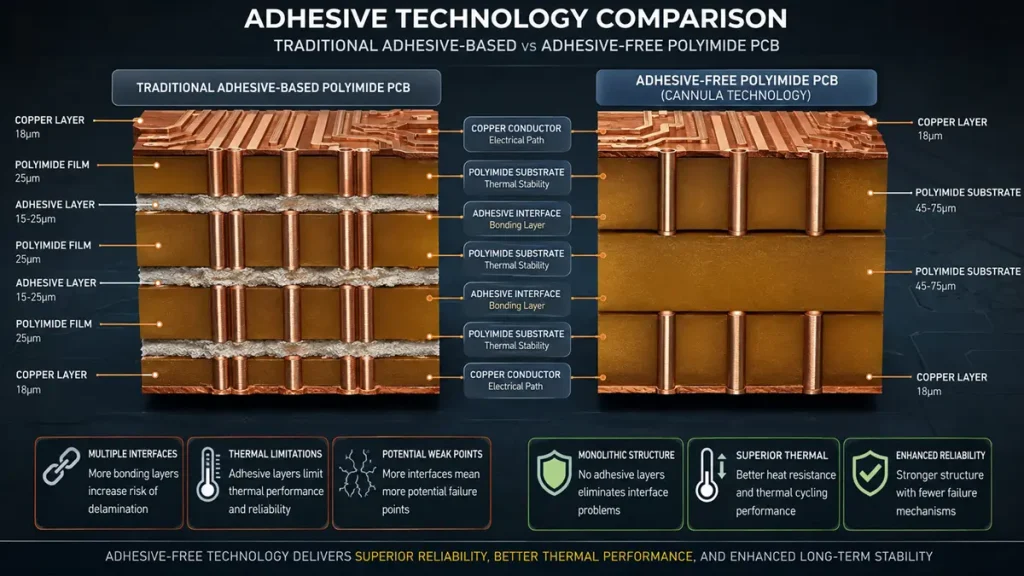
Layer Stack-Up Comparison — Traditional Adhesive-Based vs. Adhesive-Free Polyimide PCB Construction
The dominant trend in polyimide flexible circuit board manufacturing is the shift from adhesive-based to adhesive-free polyimide PCB construction. Traditional three-layer constructions (polyimide-adhesive-copper) introduce an additional material interface that increases dielectric thickness, raises thermal expansion mismatch risk, and can outgas under vacuum or high-temperature conditions.
Adhesive-free laminates bond copper directly to the polyimide substrate through casting or plasma-enhanced lamination. For procurement teams, this translates into:
- Reduced overall thickness—critical for wearable electronics and miniaturized medical devices
- Improved dimensional stability—essential for fine-pitch component alignment during SMT assembly
- Better high-frequency performance—lower dissipation factor and more consistent dielectric constant across temperature
- Enhanced thermal cycling resistance—fewer material interfaces means fewer points of delamination failure
When evaluating a polyimide flexible circuit manufacturer, ask for material traceability records specifying the laminate supplier (e.g., DuPont, Panasonic, Taiflex), whether the construction is adhesive or adhesiveless, and the qualified copper type—rolled annealed (RA) copper for dynamic flexing, or electrodeposited (ED) copper for cost-optimized static applications.
HDI Microvia and mSAP Fabrication for Miniaturized Polyimide Designs

Precision HDI Microvia & mSAP Trace Fabrication on Flexible Polyimide Substrates
Miniaturization is pushing polyimide rigid-flex PCB and flexible polyimide PCB designs into HDI territory. Laser-drilled microvias with diameters below 100 μm now appear routinely in smartphone hinge circuits, medical endoscopes, and automotive sensor modules. The 2026 state-of-the-art includes:
- UV/CO₂ laser drilling systems achieving 50–75 μm blind vias in polyimide flex layers with ±5 μm positional accuracy
- Sequential lamination enabling 3+N+3 and Any-Layer HDI structures in rigid-flex configurations
- mSAP (modified semi-additive process) producing 20 μm/20 μm line/space in production, with 8 μm/8 μm qualified for substrate-like PCB applications
For buyers sourcing rigid-flex polyimide PCB with HDI microvias, the qualification questions are specific: What is the supplier’s actual microvia aspect ratio limit for copper-filled blind vias? What is their layer-to-layer registration accuracy across the rigid-to-flex transition zone? Do they perform 100 % 3D X-ray inspection on stacked microvia structures, or rely on sampling?
A supplier quoting HDI capability without documented microsection data, IST (Interconnect Stress Test) records, or IPC-6012 Class 3 inspection protocols is presenting aspiration, not evidence.
High-Frequency Polyimide PCB Materials for 5G, 6G, and Automotive Radar
As communication and sensing systems push into millimeter-wave bands, high-frequency polyimide PCB manufacturing has become a distinct discipline. The global 5G subscriber base surpassed 2.1 billion connections in early 2026, and automotive radar modules at 77 GHz are now standard equipment in new vehicle platforms. These applications demand substrates with:
- Stable dielectric constant (Dk) and ultra-low dissipation factor (Df < 0.003 at 10 GHz)
- Thermal expansion coefficients matched to copper foil to prevent via barrel cracking
- Near-zero moisture absorption to avoid Dk drift in humid environments
While PTFE-based laminates (Rogers, Taconic) dominate pure RF applications, polyimide copper-clad laminates remain essential in hybrid rigid-flex designs where flexibility, high-temperature soldering, and controlled impedance must coexist. Advanced formulations—such as Panasonic Megtron 6/7/8 and Isola Tachyon—are increasingly specified for AI server backplanes and 5G base station flex-rigid interconnects where signal integrity cannot be compromised.
Procurement teams should confirm that the fabricator maintains qualified material inventory with incoming inspection data for Dk/Df at the operating frequency, not just manufacturer datasheet values.
AI-Assisted Inspection and Digital Manufacturing in Polyimide PCB Production
The practical value of factory automation for polyimide PCB manufacturing lies in defect detection and process traceability, not marketing buzzwords. Polyimide substrates are thin, dimensionally sensitive, and prone to handling damage. Automated systems now address specific pain points:
- AOI (Automated Optical Inspection) with machine-vision algorithms detecting fine-line opens and coverlay misregistration in flex areas
- 3D AXI (Automated X-Ray Inspection) identifying voids as small as 5 % of microvia volume in copper-filled blind vias
- AI-driven ERP scheduling optimizing production flow and reducing lead-time variance between prototype and mass production
For the buyer, the question is not whether the factory uses “AI.” The question is whether the inspection data is retained per lot, whether the customer receives microsection photographs with first-article reports, and whether the supplier can provide corrective-action documentation when a process drifts out of specification.
The Four-Stage Polyimide PCB Procurement Decision Chain
Stage 1 – Engineering Qualification: Verifying Polyimide PCB Manufacturing Feasibility
At the engineering stage, the buyer’s objective is to determine whether the design can be manufactured reliably. Send a complete RFQ package including Gerber or ODB++ files, stack-up drawings, material specifications, and mechanical requirements. A qualified polyimide PCB manufacturer should review:
- Bend radius and flex area geometry: Static bend, dynamic flex, or flex-to-install? Each requires different copper thickness, coverlay material, and conductor pattern orientation.
- Rigid-flex transition design: Are the transition zones properly supported? Is copper imbalance controlled to prevent warpage during lamination?
- Impedance targets and material selection: Does the proposed polyimide construction support the required Dk/Df and thickness tolerance?
- Microvia and via-in-pad feasibility: For HDI rigid-flex designs, can the supplier reliably plate and fill microvias in the thin dielectric layers without voids?
Hongda’s engineering team provides complimentary DFM reviews with 24-hour turnaround for standard builds and 48-hour feedback for complex rigid-flex or high-layer-count designs. This early engagement typically identifies 3–5 manufacturability optimizations before tooling is cut, preventing costly respins.
Stage 2 – Quality and Reliability Evaluation: Beyond the Sample Board
Quality managers need evidence of process control, not promises. Request the following documentation from any high-reliability polyimide PCB supplier:
- First-article inspection reports with dimensional, electrical, and microsection data
- Cross-sectional photographs showing copper wrap thickness, via fill quality, and trace geometry
- Thermal cycling or IST test results for the specific via structure and material stack-up
- Impedance coupon data verified by TDR (Time Domain Reflectometry)
- IPC Class 3 or Class 3A inspection records, depending on application criticality
- Material certificates and lot traceability from raw laminate through finished board
For automotive or medical applications, verify certifications directly: IATF 16949 for automotive, ISO 13485 for medical devices, and AS9100D for aerospace. Request the certificate number and confirm it with the issuing registrar. A supplier unwilling to provide this documentation during qualification is unlikely to maintain it during production.
Stage 3 – Commercial and Supply-Chain Review: Total Landed Cost vs. Unit Price
Purchasing teams often discover that the lowest unit price carries hidden costs. When comparing polyimide PCB suppliers in China, evaluate:
- Total landed cost: Include tooling, shipping, customs, and potential rework or field-failure liability
- Material availability and lead time: Specialty polyimide laminates may require 4–6 weeks procurement; does the supplier stock qualified materials?
- Prototype-to-production continuity: Will the same engineering team manage the transition, or does knowledge transfer fail between departments?
- Minimum order quantity and scaling flexibility: Can the supplier support both 5-piece prototypes and 10,000-piece annual volumes without process changes?
- Engineering change management: How are design revisions documented, quoted, and implemented?
Hongda operates an AI-driven ERP tracking system with an on-time delivery rate exceeding 95 %, providing real-time visibility into work-in-progress status, quality hold points, and shipping logistics. This transparency eliminates the black-box syndrome that plagues many offshore PCB procurement relationships.
Stage 4 – Management Approval: Building a Long-Term Polyimide PCB Partnership
Management decision-makers need confidence that the supplier can support future growth and product evolution. The final evaluation should cover:
- Company stability and production capacity: Facility size, employee count, equipment age, and capital investment plans
- Industry experience in your specific market: Has the supplier produced polyimide PCBs for aerospace, automotive, medical, or telecommunications applications similar to yours?
- Response-time commitments: Dedicated account management, 24/7 technical support, and escalation paths for quality issues
- Prototype-to-mass-production procedures: Is there a documented freeze process after prototype approval, or does each production lot require re-qualification?
Shenzhen Hongda Circuit Technology maintains a 30,000 m² manufacturing facility with 300+ employees, serving over 10,000 global customers across 60 countries. The company’s client list includes Intel, NXP, Texas Instruments, Continental, and Boston Scientific—indicating a track record of meeting the documentation, traceability, and reliability standards demanded by tier-one OEMs.
Why Shenzhen Hongda Circuit Technology for Polyimide PCB Sourcing
Verified Equipment and Process Capability for Polyimide, Rigid-Flex, and HDI Production
Marketing language about “advanced equipment” means little without measurable outcomes. Hongda’s 2026 manufacturing infrastructure includes specific systems relevant to polyimide PCB manufacturing and rigid-flex PCB fabrication:
| Manufacturing Area | Equipment / Capability | Buyer-Relevant Outcome |
|---|---|---|
| Laser Drilling | Mitsubishi UV/CO₂ laser systems | 50–100 μm microvias in polyimide flex layers; ±5 μm positional accuracy |
| LDI Imaging | SCREEN Ledia systems | ±1.5 μm registration accuracy; zero photomask for rapid prototyping |
| Fine-Line Processing | mSAP production line | 20 μm/20 μm line/space in production; 8 μm/8 μm qualified for SLP |
| Lamination | LAUFFER press with real-time feedback | Controlled temperature/pressure profiles for polyimide rigid-flex bonding |
| Plating | 3-in-1 horizontal line (desmear + electroless + electrolytic) | Uniform copper deposition; void-free microvia filling |
| Inspection | Nordson DAGE 3D X-ray | 5 % void detection sensitivity in filled microvias |
| Electrical Test | In-house flying probe + TDR systems | 100 % electrical coverage; ±5 % impedance verification |
| PCBA Assembly | SMT lines with BGA capability | Turnkey PCB + assembly from one source; reduced interface risk |
This equipment list is only valuable because it is paired with documented process control. Hongda’s default production standard for HDI and rigid-flex builds is IPC-6012 Class 3, with Class 3A available for aerospace applications. Certifications include ISO 9001, IATF 16949, ISO 13485, AS9100D, and UL recognition.
From Prototype to Mass Production: A Controlled Transition Path
The most expensive polyimide PCB is one that works in prototype but fails in volume. Hongda structures the transition as follows:
- Design review and DFM: Gerber, stack-up, and mechanical drawings analyzed for manufacturability risks
- Material qualification: Polyimide laminate, copper type, and adhesive system confirmed and documented
- Prototype build: 5–10 units with full first-article inspection, microsection, and electrical test data
- Process freeze: Approved stack-up, drill files, and plating parameters locked under change control
- Pilot production: Yield and Cpk validation at production parameters
- Mass production: SPC monitoring with automated data collection and lot traceability
This controlled path prevents the common failure mode where a prototype supplier improvises process parameters, only to discover at volume that registration accuracy, coverlay adhesion, or impedance tolerance cannot be maintained repeatably.
Polyimide PCB RFQ Checklist and Buyer FAQs
Before issuing an RFQ, ensure your package includes:
- Gerber or ODB++ files and layer stack-up drawing
- Material specification (polyimide type, adhesive/adhesiveless, copper weight)
- Bend radius, flex area definition, and dynamic/static flex requirements
- Impedance targets and operating frequency
- Surface finish requirements (ENIG, ENEPIG, OSP, immersion tin)
- Testing requirements (electrical, microsection, thermal cycling, IST)
- Target quantities and delivery schedule
- Required certifications (IPC class, automotive, medical, aerospace)
Frequently Asked Questions
How do I choose a reliable polyimide PCB manufacturer?
Compare the supplier’s actual material experience, fabrication tolerances, inspection systems, certifications, reliability testing, engineering response, and prototype-to-production process. Ask for measurable capability data—microvia aspect ratios, LDI registration accuracy, mSAP line/space yield, and IPC Class 3 inspection records—rather than relying on a general “polyimide PCB supplier” claim.
What information should I include in a polyimide PCB RFQ?
Provide fabrication files, stack-up, material construction, copper thickness, surface finish, coverlay or solder-mask requirements, bend radius, operating temperature, impedance targets, quantities, testing requirements, and delivery schedule. Complete information allows the manufacturer to quote accurately and identify technical risks—such as unmanufacturable bend areas or copper imbalance—before tooling is committed.
Is adhesive-free polyimide PCB better than adhesive-based flexible PCB?
Neither construction is universally superior. Adhesive-free polyimide PCB offers thinner profiles, improved dimensional stability, and better high-frequency performance, making it preferable for aerospace, medical, and high-speed designs. Adhesive-based materials may be more cost-effective and widely available for standard consumer flex circuits. The choice should be driven by electrical, mechanical, thermal, and reliability requirements—not by default.
Can Hongda manufacture HDI, microvia, high-frequency, or rigid-flex polyimide PCBs?
Yes. Shenzhen Hongda Circuit Technology publicly maintains capabilities covering high-end PCB R&D and manufacturing, high-frequency polyimide PCB production for applications above 1 GHz, complex PCBA assembly, and microvia/mSAP HDI fabrication with Any-Layer interconnect capability. Confirm the exact polyimide stack-up, minimum feature size, layer count, flex construction, and inspection requirements during the engineering review to ensure alignment with your specific design.
How can I reduce the risk of delays when sourcing polyimide PCBs from China?
Send complete design data with clear acceptance criteria before quotation. Approve the material system and construction type in writing. Request a documented first-article inspection with microsection and electrical test data. Establish direct communication contacts for engineering and quality escalation. Confirm lead times for specialty polyimide laminates, tooling, prototypes, production, inspection, and international shipping. A supplier with an AI-driven ERP system and dedicated account management—such as Hongda—provides real-time visibility that mitigates the uncertainty common in offshore procurement.
Moving from Supplier Lists to Verified Capability
The polyimide PCB market in 2026 offers more material options, finer feature capabilities, and denser interconnect technologies than ever before. For procurement teams, this abundance creates a paradox: more suppliers claim capability, but fewer can prove it through documented process control, certified quality systems, and transparent production data.
The strongest procurement position is not built on collecting quotes. It is built on staging the evaluation—engineering qualification, quality verification, commercial review, and management approval—and demanding evidence at each gate. Shenzhen Hongda Circuit Technology Co., Ltd. operates under the Hongda Circuit brand with a manufacturing infrastructure, certification portfolio, and integrated PCB + PCBA service model designed to support this evidence-based approach.
Ready to evaluate your polyimide PCB project?
Submit your Gerber files, stack-up requirements, and specifications for a complimentary DFM review and detailed quotation.
📧 Sales:sales@pcbkr.com
📧 Engineering:pcb@pcbkr.com
📞 Phone: +86 0755 23720053
🌐 Website:www.pcbkr.com
📍 Address: Room 1608-1610, Research Development Comprehensive Building, Baoyunda Logistics Center, Baoan, Shenzhen, China
About Author
David Chen https://www.linkedin.com/in/pcbcoming
David Chen boasts an extensive professional background in PCBA manufacturing, PCBA testing, and PCBA optimization, with specialized expertise in high-precision PCBA fault analysis and rigorous PCBA reliability testing. The author has worked with high-layer-count server PCB fabrication, ultra-low-loss backplane stackups, and thermo-mechanical reliability optimization for AI infrastructure projects involving 112G and 224G PAM4 architectures. Skilled in complex circuit design and cutting-edge advanced PCB manufacturing processes, he delivers solutions that elevate product durability and performance across industrial applications. His technical articles focusing on PCBA manufacturing workflows and testing methodologies are widely cited by industry peers, research institutions, and technical platforms, solidifying his reputation as a recognized technical authority in the global circuit board manufacturing sector.