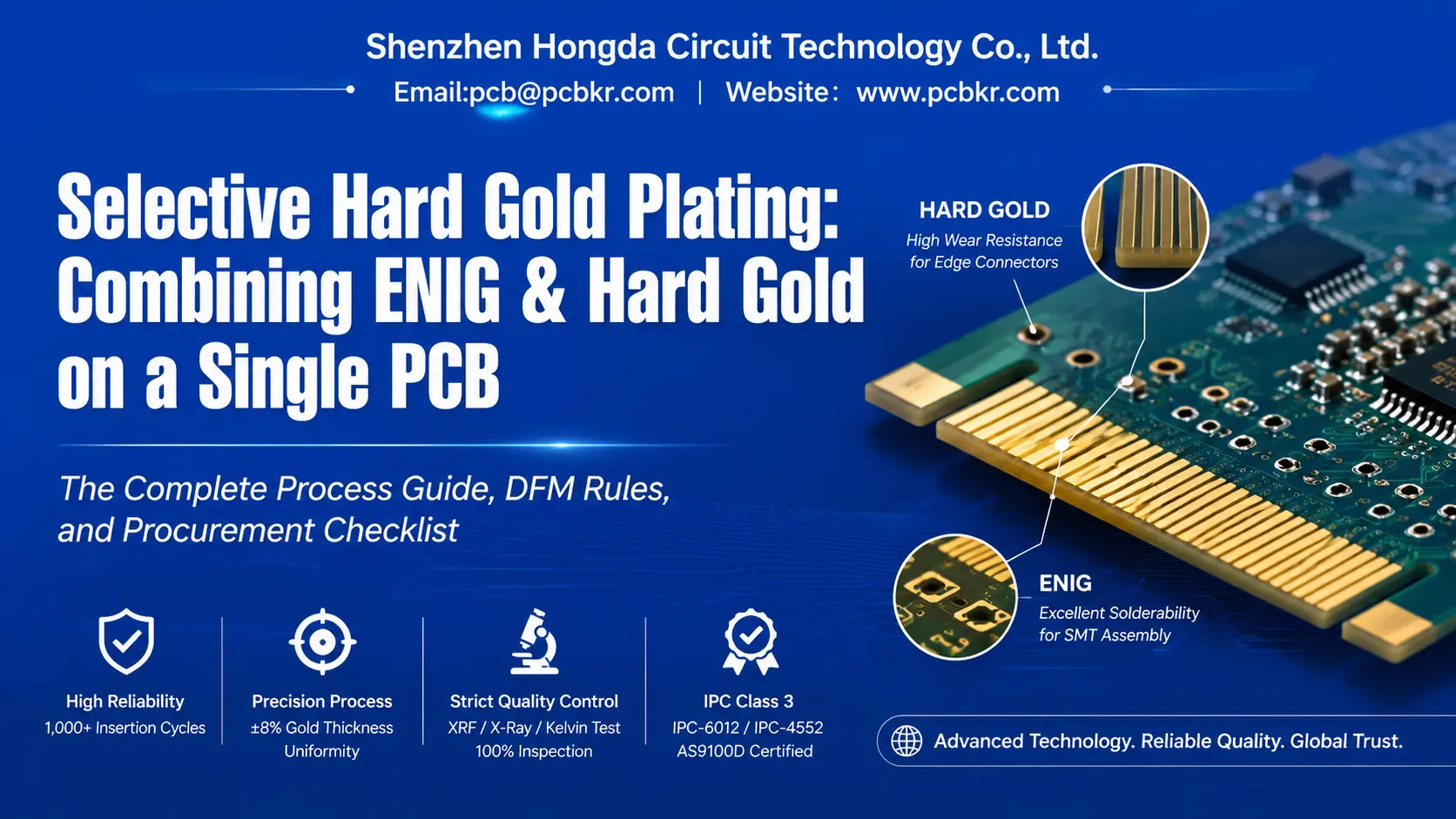
Selective Hard Gold Plating: Combining ENIG & Hard Gold on a Single PCB
Why Selective Hard Gold? Solving the SMT Solderability vs. Edge Connector Wear Resistance Dilemma
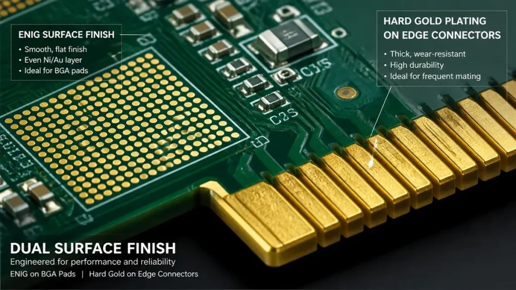
Dual Surface Finish PCB: ENIG BGA Pads & Hard Gold Edge Connectors
Modern PCB designs rarely demand a single surface finish across the entire board. A typical high-reliability board—whether an AI server accelerator card, a military VPX backplane, or an automotive ECU interface—must simultaneously satisfy two contradictory requirements: flawless solderability on BGA lands for SMT assembly, and extreme wear resistance on edge connector gold fingers that endure thousands of insertion cycles.
Electroless Nickel Immersion Gold (ENIG) delivers exceptional solderability for fine-pitch components, but its thin gold layer (0.05–0.1 µm) wears off within 1–10 mating cycles, exposing the nickel underlayer to oxidation and contact failure. Conversely, electroplated hard gold—typically 0.5–3.0 µm thick with cobalt or nickel alloy hardeners—provides the durability demanded by PCIe Gen 6 and VPX connectors, yet its alloyed composition creates brittle solder joints when applied to SMT pads.
The solution is selective hard gold plating: a hybrid surface finish strategy that confines electrolytic hard gold strictly to high-wear contact zones while preserving ENIG on all solderable lands. This approach is not merely a cost-saving tactic—it is a reliability engineering decision that separates commodity fabricators from manufacturers qualified for IPC-6012 Class 3 and AS9100D programs.
At Shenzhen Hongda Circuit Technology Co., Ltd., our 2026-spec selective plating line processes boards up to 24″ panel size with ±8% gold thickness uniformity, validated by 50 µm micro-focus XRF on every production lot. The result is a board that solders beautifully during assembly and survives 1,000+ insertion cycles in the field.
The Hybrid Manufacturing Challenge: ENIG on SMT Pads + Electroplated Hard Gold on Gold Fingers
Combining two distinct metallization chemistries on one substrate introduces process interactions that unqualified suppliers routinely mishandle. The core challenge lies in sequencing: hard gold electroplating is an electrolytic process requiring cathodic current distribution through temporary bus bars, while ENIG is a purely chemical immersion process that deposits uniformly across all exposed copper.
If the manufacturing sequence is wrong, three failure modes emerge:
Nickel-Gold Bridge Defects: Electrolytic bath chemistry can wick under solder mask dams, creating conductive bridges between adjacent gold fingers or between a finger and a nearby copper trace. These bridges often measure only 10–50 µm wide—undetectable by standard AOI but catastrophic during connector mating.
Solder Mask Lifting: The aggressive pH and temperature of hard gold electrolytes (typically 50–65°C) can degrade solder mask adhesion if the mask is not fully cured or if the dam width is insufficient. Once the mask lifts, plating chemistry infiltrates beneath, causing undercut corrosion of the copper trace.
Residual Plating Bus Contamination: Every hard gold pad must remain electrically connected to the plating cathode during deposition. If the temporary bus bar (tie-bar) is not designed for clean removal, residual copper stubs protrude beyond the board edge, interfering with connector polarization keys or creating short circuits between adjacent fingers.
These risks explain why selective hard gold PCB procurement requires supplier qualification beyond standard ISO 9001. The fabricator must demonstrate dedicated hard gold infrastructure—not a shared ENIG line with manual masking—and in-house microsection capability to verify nickel barrier integrity.
Step-by-Step Selective Hard Gold Plating Manufacturing Workflow

Automated PCB Hard Gold Electroplating Line at Hongda Circuit
Step 1: Dry Film Masking and Selective Copper Etching
The process begins after inner-layer lamination, drilling, and electroless copper deposition. The panel enters the outer-layer imaging stage, where dry film photoresist is laminated and exposed using direct LDI imaging. For selective hard gold designs, two imaging steps are required:
First, the primary circuit pattern is imaged and plated with standard electrolytic copper (25–35 µm) and tin etch resist. Then, a secondary dry film mask is applied specifically to protect non-contact areas during the subsequent hard gold plating sequence. At Shenzhen Hongda Circuit Technology, our SCREEN Ledia LDI systems achieve ±10 µm registration accuracy—critical for maintaining the 0.15 mm minimum solder mask dam width between gold-plated regions and adjacent copper conductors.
After pattern plating, the tin resist is stripped and exposed copper is etched. For selective gold designs, the etch chemistry must be tightly controlled to prevent undercut beneath the gold fingers; excessive undercut creates slivering or flaking of the nickel-gold stackup during edge beveling.
Step 2: Bus-Bar Routing and Selective Electroplating
This is the most process-critical stage. Every gold finger pad must be electrically continuous with the panel edge to receive plating current. Two primary methods exist:
Method A: Full-Panel Plating with Flash Etch The entire panel receives nickel-gold electroplating through a continuous bus network. Photoresist masking protects non-contact areas, and a subsequent flash etch removes gold from solder lands. This method ensures uniform current distribution but consumes more gold and requires precise masking alignment.
Method B: Spot Plating with Laser-Aligned Masking Gold is deposited only on designated contact arrays, with automated optical alignment ensuring ±0.05 mm boundary precision. This method eliminates plating bus remnants on sensitive RF traces and is preferred for boards with high-density routing near the connector edge.
At our facility, the plating line uses pulse-reverse electrolytic gold deposition. The nickel underplate—100–300 µin thick with <100 ppm organic contamination—provides the barrier against copper diffusion and the structural hardness for contact durability. The gold layer is deposited at 15–80 µin thickness depending on the application specification, with cobalt alloy (130–200 HK) providing the wear resistance required by IPC-4552.
Critical process controls during this stage include:
- Current density uniformity: ±5% across the panel, verified by cathode current distribution modeling
- Bath temperature: 55°C ±2°C, with continuous filtration to prevent particulate inclusion
- Plating bar (thieving busbar) design: ≥1.0 mm width to prevent current crowding, located outside the final board outline
Step 3: Stripping, Secondary ENIG Immersion, and Final Finishing
After hard gold deposition, the temporary plating resist is stripped, and the panel enters the ENIG immersion line. This is where the hybrid finish is realized: the gold fingers retain their electrolytic hard gold, while all other exposed copper lands receive the electroless nickel (3–6 µm) and immersion gold (0.05–0.1 µm) stackup.
The ENIG process must be sequenced to avoid contaminating the hard gold surface. At Shenzhen Hongda Circuit Technology, we operate dedicated ENIG and hard gold lines with separate waste treatment systems—cross-contamination between chemistries is a common root cause of black pad failure in hybrid-finish boards.
Following surface finishing, the panel undergoes:
- CNC precision beveling: 20°–45° chamfer angles with ±0.5° tolerance, using diamond-coated tools to achieve Ra <0.4 µm edge smoothness
- 100% contact resistance testing: Four-wire Kelvin measurement on every production panel, with rejection criteria set at <20 mΩ per IPC-6012 Class 3
- 3D X-Ray inspection: Nordson DAGE X-Ray systems verify inner-layer alignment and detect microvoids in the nickel barrier
The Schmoll MX-500 profile router removes plating tie-bars with ±0.025 mm accuracy, followed by automated edge polishing. For medical and aerospace designs requiring absolute zero residual, we specify tab routing with mouse-bite breakaway, ensuring the tie-bar breaks flush with the board edge.
DFM Rules for Selective Plating: Avoiding Nickel-Gold Bridge Defects
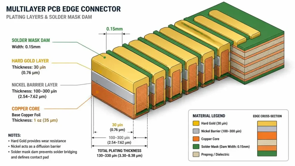
3D Cross-Section Diagram of Selective Hard Gold PCB Plating & DFM Rules
Procurement teams evaluating selective hard gold PCB suppliers should verify that the fabricator enforces these DFM rules during pre-production review:
Solder Mask Dam Integrity Maintain ≥0.15 mm (6 mil) solder mask dam width between gold-plated regions and adjacent copper conductors. Narrower dams risk chemical seepage during plating, causing nickel undercut or black pad precursor conditions. Our LDI imaging systems achieve ±10 µm solder mask registration, ensuring a 0.1 mm minimum mask pullback from the gold finger edge without exposing adjacent circuitry.
Plating Tie-Bar Design and Removal Tie-bars must connect at the root of the finger (board-edge side), not the tip, to minimize post-removal cleanup. Specify CNC routing for cleanest edges; V-scoring leaves slight residual nubs that can interfere with connector insertion. Residual copper protrusion tolerance is 0.0 mm—any protrusion creates short risk and insertion interference.
Gold-to-Copper Spacing Maintain ≥0.25 mm clearance between selective gold areas and exposed copper traces to prevent electrolytic bridging during bath immersion. This rule is especially critical for boards with RF traces routed near the connector edge.
Inner-Layer Copper Peel Strength For high-insertion-cycle designs, inner-layer copper peel strength must be ≥1.05 N/mm per IPC-TM-650 2.4.8. Use high-Tg (≥170°C) laminate to reduce thermal expansion mismatch between the FR-4 core and the copper/nickel/gold stackup during reflow.
Beveling and Edge Quality Gold fingers require edge chamfering at 20°, 30°, or 45° (±2° tolerance). For boards >3.2 mm thick, consider adding a 0.5 mm unfilled fiberglass edge band to absorb insertion shock. Our CNC beveling stations hold ±2° angular tolerance with 0.05 mm edge radius control.
Three-Tier Keyword Matrix for SEO and Content Strategy
Tier 1: Core Target Keywords (High Search Volume, High Competition)
- selective hard gold pcb
- hard gold plating pcb process
- hybrid pcb surface finish
- electroplated hard gold pcb
- gold finger pcb manufacturing
Tier 2: Derivative and Long-Tail Keywords (Medium Competition, High Purchase Intent)
- selective gold plating process guide
- ENIG hard gold combination pcb
- hard gold vs ENIG edge connectors
- selective hard gold plating DFM rules
- nickel gold bridge defect prevention
- plating bus bar routing pcb
- pulse reverse electrolytic gold plating
- hard gold plating thickness specification
Tier 3: Niche and Application-Specific Keywords (Low Competition, High Conversion)
- selective hard gold for PCIe Gen 6 cards
- hybrid surface finish military VPX backplane
- automotive ECU gold finger pcb supplier
- IPC-4552 hard gold plating certification
- selective gold plating with mSAP process
- 224G PAM4 gold finger pcb manufacturing
- AS9100D selective hard gold supplier China
Frequently Asked Questions: Selective Hard Gold PCB Procurement
How do I verify that a PCB supplier can reliably produce hybrid ENIG + hard gold finishes?
Request documentation of dedicated hard gold plating lines separate from ENIG immersion baths. Verify certifications including IPC-6012 Class 3, IPC-4552, and AS9100D. Ask for microsection photographs showing nickel barrier integrity and gold thickness uniformity. A qualified supplier should provide XRF thickness reports on every production lot, not just first articles. At Shenzhen Hongda Circuit Technology, we maintain separate waste treatment systems for hard gold and ENIG chemistries to prevent cross-contamination.
What is the typical cost premium for selective hard gold compared to full-board ENIG?
The premium depends on gold finger length, panel utilization, and thickness specification. Selective plating typically adds 15–35% to board cost versus ENIG-only, but this is far lower than full-body hard gold which can double the price. The key cost driver is gold thickness: 30 µin gold adds modest cost, while 80 µin heavy hard gold for military applications increases material cost significantly. Spot plating with laser-aligned masking minimizes gold consumption by restricting deposition strictly to contact pads.
Can selective hard gold be applied to areas other than edge connectors?
Yes. Selective hard gold is routinely applied to test point pads, keypad contacts, and sliding switch interfaces located in the board interior. This requires either dry film masking with flash etch or spot plating with automated optical alignment. The design must include temporary plating bus bars routed to the panel edge, with sacrificial tabs removed post-plating. Maintain ≥0.25 mm clearance between selective gold areas and exposed copper traces to prevent electrolytic bridging.
What storage and handling protocols preserve hybrid-finish PCB solderability and shelf life?
Store boards in vacuum-sealed bags with desiccant at <30% RH and 15–25°C. For boards with mixed ENIG + hard gold finishes, solderability shelf life is dictated by the ENIG regions (typically 12 months per IPC-4552). Hard gold contact areas remain insertion-ready for 24+ months if protected from mechanical abrasion during handling. Avoid sulfur-containing packaging materials, as sulfur reacts with gold surfaces to form insulating sulfide films.
What are the critical inspection checkpoints I should specify in my purchase order for selective hard gold boards?
Specify: (1) 100% XRF gold thickness verification with ±8% uniformity; (2) four-wire Kelvin contact resistance testing <20 mΩ per finger; (3) microsection analysis of nickel barrier thickness (100–300 µin) and gold thickness; (4) solder mask dam integrity inspection at ≥0.15 mm width; (5) CNC beveling angle verification within ±2° tolerance; and (6) residual tie-bar protrusion at 0.0 mm. These checkpoints ensure the board meets both solderability and insertion-cycle requirements without field failures.
Shenzhen Hongda Circuit Technology Co., Ltd. manufactures IPC-Class-3 selective hard gold PCBs from prototype to mass production, with in-house electroplating, precision beveling, and XRF verification. Our 2026 equipment lineup—including SCREEN Ledia LDI, Mitsubishi laser drilling, and Nordson DAGE X-Ray inspection—delivers the precision that high-reliability connectors demand. Submit your Gerber files and plating specifications to sales@pcbkr.com for a complimentary DFM review and detailed quotation within 30 minutes.
About Author
David Chen https://www.linkedin.com/in/pcbcoming
David Chen boasts an extensive professional background in PCBA manufacturing, PCBA testing, and PCBA optimization, with specialized expertise in high-precision PCBA fault analysis and rigorous PCBA reliability testing. The author has worked with high-layer-count server PCB fabrication, ultra-low-loss backplane stackups, and thermo-mechanical reliability optimization for AI infrastructure projects involving 112G and 224G PAM4 architectures. Skilled in complex circuit design and cutting-edge advanced PCB manufacturing processes, he delivers solutions that elevate product durability and performance across industrial applications. His technical articles focusing on PCBA manufacturing workflows and testing methodologies are widely cited by industry peers, research institutions, and technical platforms, solidifying his reputation as a recognized technical authority in the global circuit board manufacturing sector.