Hard Gold PCB Manufacturing & Plating Guide: IPC Standards, Selective Plating Design, and Sourcing Strategy for High-Reliability Interconnects
What Is Hard Gold PCB and How Does It Differ from ENIG?
1.1: Defining Electroplated Hard Gold on PCBs
When hardware engineers specify a Hard Gold PCB, they are referring to an electrolytically deposited gold-nickel alloy coating—typically hardened with cobalt or nickel additives—applied over an electrolytic nickel underlayer. Unlike the soft, immersion-deposited gold used in ENIG (Electroless Nickel Immersion Gold), hard gold is engineered for mechanical endurance. The Knoop hardness ranges from 130 to 200 HK, depending on the alloy composition and bath chemistry, making it the only viable surface finish for edge connectors, gold fingers, and keypad contacts that must survive thousands of insertion cycles.
At Shenzhen Hongda Circuit Technology Co., Ltd., our plating lines deposit hard gold thickness from 10 µin to 100 µin (0.25 µm to 2.54 µm) over a sulfamate nickel barrier of 100 µin to 200 µin minimum. This dual-layer architecture serves two non-negotiable functions: the nickel acts as a diffusion barrier preventing copper-gold intermetallic growth, while the hardened gold topcoat withstands abrasive wear and maintains contact resistance stability across the product lifecycle.
1.2: Hard Gold vs ENIG — Engineering Parameter Comparison
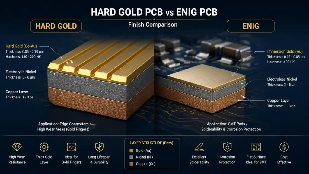
3D Cross-Section Comparison Between Hard Gold and ENIG PCB Finishes
The confusion between hard gold vs ENIG costs procurement teams thousands in redesigns. ENIG deposits a thin immersion gold layer (typically 0.05–0.125 µm) over electroless nickel. It excels at solderability and fine-pitch BGA pad coverage, but its hardness sits below 90 HK—too soft for mechanical sliding contact. Hard gold, conversely, requires an electrical bus line for electroplating current, demands selective masking for non-contact areas, and carries a solderability risk if over-applied to SMT lands.
| Engineering Parameter | Hard Gold (Electroplated) | ENIG (Immersion Gold) |
|---|---|---|
| Gold Hardness | 130–200 HK (Cobalt/Nickel alloyed) | < 90 HK (Pure soft gold) |
| Typical Thickness | 15–50+ µin (0.38–1.27 µm) | 1.97–5 µin (0.05–0.125 µm) |
| Primary Application | Edge connectors, gold fingers, keypads | SMT pads, BGA, fine-pitch components |
| Solderability | Poor on thick deposits; embrittlement risk >3% Au | Excellent; optimized for reflow |
| Wear Resistance | > 1,000 insertion cycles at 30 µin | Low; unsuitable for mechanical mating |
| Deposition Method | Electrolytic (requires plating buss) | Chemical/electroless (no buss) |
| Relative Cost | 60–120% premium over bare copper edges | 25–45% premium over bare copper |
1.3: IPC-4552 Classification Context
While IPC-4552B primarily governs ENIG finishes, its 2021 revision established measurement calibration standards that directly benefit hard gold thickness verification. The standard’s 1.5 mm × 1.5 mm measurement spot size and XRF gauge repeatability protocols are now applied uniformly across both immersion and electrolytic gold finishes in Class 3 facilities. At Shenzhen Hongda Circuit Technology Co., Ltd., our XRF stations are calibrated to IPC-4552B guard-band tolerances, ensuring that a “30 µin” specification carries the same meaning on our floor as it does in your design documentation.
2: IPC Standards and Plating Thickness Requirements for Hard Gold
2.1: IPC-6012 and IPC-4552B Compliance for Electroplated Gold
Procurement managers auditing hard gold PCB suppliers must verify adherence to IPC-6012F (rigid board qualification) and IPC-4552B (surface finish performance). For hard gold specifically, IPC-6012 Class 3 mandates:
- Gold thickness: Minimum 15 µin (0.38 µm) for standard industrial connectors; 30 µin (0.76 µm) for high-cycle applications; 50 µin+ (1.27 µm+) for military/aerospace edge connectors.
- Nickel underlayer: 100–200 µin (2.54–5.08 µm) of electrolytic sulfamate nickel to prevent copper diffusion and provide mechanical support.
- Purity: ASTM B488 requires minimum 99.0% gold content for engineering-grade coatings, with cobalt or nickel hardening agents not exceeding 0.3% by weight.
2.2: How Thick Is Hard Gold Plating on PCBs? Application-Driven Tiers
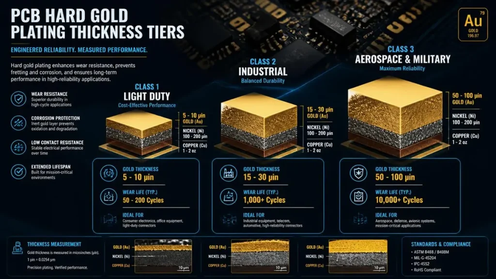
PCB Hard Gold Plating Thickness Tiers and Insertion Life Cycles (Class 1 to Class 3)
The question “how thick is hard gold plating PCB” has no single answer—it depends on insertion cycle requirements and environmental stress. At Shenzhen Hongda Circuit Technology, we segment production into three tiers:
| Application Class | Gold Thickness | Insertion Life | Typical Use Case |
|---|---|---|---|
| Class 1 (Light friction) | 5–10 µin (0.125–0.25 µm) | 50–200 cycles | Test fixtures, low-cycle programming headers |
| Class 2 (Standard industrial) | 15–30 µin (0.375–0.76 µm) | 1,000–2,000 cycles | PCIe slots, industrial backplanes, DDR5 modules |
| Class 3 (High-reliability) | 50–100 µin (1.27–2.54 µm) | 10,000+ cycles | Aerospace card guides, military radios, medical device docking stations |
Our Nordson DAGE X-Ray fluorescence systems verify every lot against customer specifications, with Cpk targets exceeding 1.33 on thickness uniformity. For context, a 30 µin hard gold finger on a properly nickel-backed edge connector will typically survive 1,000–2,000 insertion/withdrawal cycles without exposing the nickel sub-layer—assuming standard contact force and chamfer geometry.
2.3: Measurement Methodology and Quality Gates
XRF (X-ray Fluorescence) is the production-standard method for non-destructive hard gold thickness verification. However, IPC-4552B cautions that XRF readings vary between instruments and operators, necessitating gauge repeatability studies and inter-lab correlation. At Shenzhen Hongda Circuit Technology Co., Ltd., we maintain a master calibration protocol traceable to NIST standards, with daily drift checks using certified gold foils. Cross-sectional SEM analysis is performed on first articles and quarterly process audits to validate XRF correlation.
3: Designing with Selective Hard Gold Plating
3.1: Can Hard Gold Be Selectively Used on a PCB in the Center of the Board?
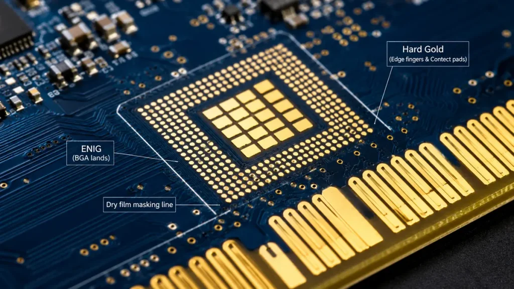
Macro Demonstration of Selective Hard Gold Plating vs. ENIG BGA Lands
Yes. Selective hard gold plating PCB design is not only feasible—it is the dominant cost-optimization strategy for boards mixing high-wear contacts with solderable SMT areas. The technique applies electrolytic gold strictly to contact pads, gold fingers, or edge connector regions, while leaving BGA lands and component pads in ENIG, OSP, or immersion tin. This hybrid approach answers the procurement team’s priority: maximize durability where needed, minimize gold consumption everywhere else.
At Shenzhen Hongda Circuit Technology, we execute selective plating through two primary methods:
- Dry film masking + full-panel plating: The entire panel receives nickel-gold electroplating; photoresist masking protects non-contact areas during a subsequent flash etch that removes gold from solder lands.
- Spot plating with laser-aligned masking: Gold is deposited only on designated contact arrays, with automated optical alignment ensuring ±0.05 mm boundary precision. This method eliminates plating buss remnants on sensitive RF traces.
3.2: Critical DFM Rules for Selective Hard Gold Layout
Engineers frequently underestimate the design constraints of selective gold plating PCB layouts. These rules prevent nickel corrosion, solder mask lifting, and plating bath contamination:
- Minimum solder mask dam width: ≥ 0.15 mm (6 mil) between gold-plated regions and adjacent copper conductors. Narrower dams risk chemical seepage during plating, causing nickel undercut or “black pad” precursor conditions.
- Plating buss routing: Every hard gold pad requires an electrical connection to the plating cathode. Buss lines must exit the board edge or terminate in sacrificial tabs that are mechanically removed post-plating. Design buss width at ≥ 0.3 mm to prevent fusing during high-current deposition.
- Gold-to-copper spacing: Maintain ≥ 0.25 mm clearance between selective gold areas and exposed copper traces to prevent electrolytic bridging during bath immersion.
- Beveling specification: Gold fingers require edge chamfering at 20°, 30°, or 45° (±2° tolerance) to ensure smooth insertion. At Shenzhen Hongda Circuit Technology Co., Ltd., our CNC beveling stations hold ±2° angular tolerance with 0.05 mm edge radius control.
3.3: Cost Impact of Selective vs Full-Board Hard Gold
Selective plating reduces gold consumption by 40–70% compared to full-panel hard gold finish. For a standard PCIe card with eight gold fingers (approximately 200 mm² total contact area), selective plating consumes roughly 0.03 g of gold at 30 µin thickness. Full-board plating on the same panel size would consume 10–15× that quantity. In 2026, with gold prices sustaining upward pressure, selective design is not merely a cost-saving tactic—it is a procurement imperative.
4: Durability, Hardness Levels, and Performance Testing
4.1: Hardness Grades and Alloy Specifications
Not all electroplated gold PCB finishes wear the same. Hard gold is categorized by Knoop hardness and alloy content, historically referenced to MIL-G-45204 (now superseded by ASTM B488 and internal IPC-TM-650 test methods):
- Type I (Soft Gold): < 90 HK, pure gold. Used for wire bonding, not edge connectors.
- Type II (Hard Gold): 130–200 HK, alloyed with 0.1–0.3% cobalt or nickel. The standard for PCB gold fingers and keypad contacts.
- Type III (Extra Hard): > 200 HK, higher alloy content. Rare in standard PCB applications due to increased contact resistance; reserved for extreme-wear military connectors.
At Shenzhen Hongda Circuit Technology Co., Ltd., our sulfamate nickel + cobalt-hardened gold bath consistently delivers 150–180 HK across production lots, verified by quarterly microhardness testing per IPC-TM-650 Method 2.4.28.
4.2: Insertion Cycle Testing and Environmental Validation
Durability claims mean nothing without test data. Our quality lab subjects hard gold edge connector PCB samples to three validation protocols:
- Insertion/Withdrawal Cycling: Automated mating fixture simulates 1,000–10,000 cycles at specified contact force. Failure criteria include > 10 mΩ contact resistance increase or nickel exposure.
- Salt Spray Testing: Per ASTM B117, 5% NaCl fog at 35°C for 48–96 hours. Validates nickel barrier integrity and gold porosity.
- Thermal Shock: IPC-TM-650 Method 2.6.7, −65°C to +125°C for 100 cycles. Ensures no delamination or intermetallic cracking at the nickel-gold interface.
4.3: The Nickel Underlayer’s Hidden Role
The 100–200 µin nickel barrier is the unsung hero of hard gold plating PCB reliability. Electrolytic sulfamate nickel provides:
- Diffusion blocking: Prevents copper atoms from migrating into the gold layer, which would otherwise form brittle Cu-Au intermetallics and raise contact resistance.
- Mechanical support: The nickel’s 300–400 HK hardness supports the thinner gold layer during contact wipe, preventing sub-layer collapse.
- Corrosion resistance: Even if the gold layer is porous or worn through, the nickel provides sacrificial protection against atmospheric oxidation.
This is a fundamental distinction from ENIG, where the electroless nickel phosphorus content (typically 7–9% P) creates a different crystalline structure with lower ductility and distinct corrosion susceptibility.
5: Cost Optimization, Reliability Risks, and Alternative Finishes
5.1: Gold Price Volatility and Design-Stage Cost Control
For procurement directors, hard gold PCB cost is driven by three variables: gold thickness, plated area, and London Bullion Market Association (LBMA) spot price. In 2026, sustainability pressures and supply chain constraints continue to elevate precious metal costs. Optimizing at the design stage yields more savings than negotiating unit price:
- Reduce thickness where cycles allow: If your connector specification only requires 500 cycles, drop from 50 µin to 30 µin. This 40% thickness reduction cuts gold mass proportionally.
- Minimize selective area: Review Gerber files for “gold bleed”—unnecessary plating around contact pads that increases area by 15–20%.
- Hybrid finish strategy: Specify ENIG on SMT lands and hard gold only on fingers. This eliminates the need for secondary solder mask steps and reduces processing complexity.
5.2: Gold Embrittlement and Lead-Free Assembly Risks
Two reliability traps dominate hard gold finish PCB assembly discussions:
Gold Embrittlement: When gold dissolves into molten solder beyond ~3% by weight, it forms AuSn₄ intermetallic compounds that embrittle solder joints. This risk intensifies under lead-free reflow profiles (peak 245–260°C), where gold dissolution rates are higher than legacy tin-lead processes. The solution is strict selective plating—never allow hard gold on SMT pads that will be soldered. If rework is unavoidable, remove gold by mechanical scraping or chemical stripping before hand-soldering.
Thick Gold Hand-Soldering Challenges: Manual soldering onto 50 µin+ hard gold deposits requires excessive iron dwell time, risking pad lift or laminate damage. Design for automated selective wave soldering where possible, or specify flash gold (0.05 µm) on test points that require occasional hand-soldering.
5.3: Alternative Finishes and When to Specify Them
| Finish | Hardness | Best For | Limitation |
|---|---|---|---|
| Hard Gold (Ni/Au) | 130–200 HK | High-cycle connectors, gold fingers | Highest cost; poor solderability |
| ENEPIG | N/A (thin Au) | Wire bonding + SMT on same board | Palladium cost; complex chemistry |
| PdNi (Palladium-Nickel) | 450–550 HK | Extreme wear (relay contacts) | Higher contact resistance; limited PCB suppliers |
| Immersion Tin | Soft | Cost-sensitive, solderable areas | Short shelf life; tin whisker risk |
| OSP | N/A | Lowest cost, single-reflow boards | No contact wear resistance; limited thermal cycles |
At Shenzhen Hongda Circuit Technology Co., Ltd., we guide customers through this matrix during complimentary DFM reviews. For example, a 224G PAM4 AI server backplane with edge connector fingers and high-density BGA lands might use selective hard gold on fingers + ENEPIG on BGA pads—a hybrid we have qualified for multiple hyperscale customers.
5.4: Sustainability and Gold Recovery
Responsible PCB manufacturing now includes precious metal recycling. Our Shenzhen facility operates closed-loop gold reclamation from plating bath drag-out and rinse water, recovering > 95% of residual gold. This reduces effective material cost and aligns with customer ESG mandates for circular manufacturing.
6: Sourcing Hard Gold PCB from a Verified Manufacturer — Why Shenzhen Hongda Circuit Technology
6.1: 2026 Manufacturing Technology for Precision Gold Deposition
Selecting a China hard gold PCB supplier requires verification beyond brochure claims. At Shenzhen Hongda Circuit Technology Co., Ltd., our 2026 equipment lineup addresses the exacting requirements of PCIe Gen 6, AI server backplanes, and automotive edge connectors:
- SCREEN Ledia LDI: Laser Direct Imaging for selective plating photoresist alignment within ±8 µm, critical for fine-pitch gold finger definition.
- Mitsubishi CO₂/UV Laser Drilling: Dual-head systems for microvia formation and plating buss routing on high-layer-count boards.
- Nordson DAGE X-Ray Inspection: 3D XRF and AXI systems for 100% thickness verification and void detection in nickel underlayers.
- mSAP Production Line: Modified Semi-Additive Process enabling 30/30 µm line/space with selective gold integration—essential for substrate-like PCBs (SLP) in mobile and AI accelerator modules.
Our plating chemistry is sourced from MacDermid Alpha and Atotech formulations, with bath analysis performed every 4 hours by automated titration. This process discipline delivers Cpk > 1.33 on gold thickness uniformity across panel and lot-to-lot.
6.2: Certification Stack and Quality Infrastructure
Procurement teams in industrial, automotive, and aerospace sectors require documented compliance. Our quality system includes:
- ISO 9001:2015 and AS9100D (Aerospace)
- IPC-6012 Class 3/3A and IPC-A-600 Class 3
- ISO 13485 (Medical Devices) and IATF 16949 (Automotive)
- ITAR-compliant handling procedures for defense programs
Every hard gold plating PCB shipment includes a Certificate of Conformance, XRF thickness measurement report, cross-sectional micrograph (on request), and full electrical test data.
6.3: Procurement Workflow and DFM Partnership
We structure our engagement around the procurement decision chain:
- 30-Minute Inquiry Response: Upload Gerber and stack-up to sales@pcbkr.com. Our engineering team flags selective plating risks, buss routing conflicts, and solder mask dam violations before quoting.
- Free DFM Review: We validate bevel angles, gold finger pitch, nickel thickness compatibility, and impedance continuity—critical for high-speed edge connectors.
- First Article Validation: Proto builds include full XRF mapping, insertion cycle sampling, and cross-sectional analysis. No surprises at volume.
- Volume Scaling: From 5-piece prototypes to 10,000+ panel monthly runs, with AI-driven ERP tracking maintaining > 95% on-time delivery.
FAQ — Hard Gold PCB Procurement and Supplier Selection
How do I verify that a hard gold PCB supplier actually meets IPC-6012 Class 3 thickness requirements?
Request the supplier’s XRF calibration certificate traceable to NIST or equivalent national standards. Ask for a first-article cross-sectional micrograph showing nickel underlayer thickness, gold thickness, and interface integrity. At Shenzhen Hongda Circuit Technology Co., Ltd., we provide these documents as standard for all Class 3 orders, along with statistical process control (SPC) charts showing Cpk values for thickness uniformity.
What is the realistic lead time for selective hard gold PCB prototypes versus standard ENIG boards?
Selective hard gold adds 1–2 days to standard lead time due to the additional photoresist masking, electrolytic plating, and buss removal steps. At Shenzhen Hongda Circuit Technology, our selective hard gold prototypes ship in 5–7 days (vs. 3–5 days for ENIG), with volume production ramping to 2-week cycles depending on panel complexity and gold thickness.
Can a Chinese PCB manufacturer handle AS9100D aerospace hard gold requirements with full traceability?
Yes—provided the facility holds current AS9100D certification and maintains lot traceability from raw laminate to finished board. Shenzhen Hongda Circuit Technology Co., Ltd. operates under AS9100D with full material certification, process parameter logging, and AS9102-compliant first article inspection. We have delivered hard gold rigid-flex boards for avionics docking stations with 50 µin gold and 200 µin nickel, fully documented for OEM audit.
How should I structure my RFQ to get an accurate hard gold PCB quote without hidden costs?
Specify: (1) exact gold thickness and nickel underlayer thickness per IPC-6012 class; (2) selective plating areas with Gerber layer highlighting; (3) bevel angle and tolerance; (4) required test methods (XRF, cross-section, insertion cycle); and (5) certification level (Class 2 vs. Class 3). Vague RFQs lead to assumptions—usually in the supplier’s favor. Shenzhen Hongda Circuit Technology Co., Ltd.’s engineering team reviews every RFQ for DFM feasibility before final pricing, eliminating post-order surprises.
What storage and handling protocols preserve hard gold PCB solderability and shelf life?
Hard gold itself does not oxidize, but the nickel underlayer can form passive oxide if exposed to humidity over extended storage. Store boards in vacuum-sealed bags with desiccant at < 30% RH and 15–25°C. For boards with mixed ENIG + hard gold finishes, solderability shelf life is dictated by the ENIG regions (typically 12 months). Hard gold contact areas remain insertion-ready for 24+ months if protected from mechanical abrasion during handling.
Ready to source your next Hard Gold PCB project?
Shenzhen Hongda Circuit Technology Co., Ltd. manufactures IPC-Class-3 selective hard gold PCBs from prototype to mass production, with in-house electroplating, precision beveling, and XRF verification. Submit your Gerber files and plating specifications to sales@pcbkr.com for a complimentary DFM review and detailed quotation within 30 minutes.
Company: Shenzhen Hongda Circuit Technology Co., Ltd.
Website:www.pcbkr.com
Email:sales@pcbkr.com
Phone: +86 0755 23720053
Certifications: ISO 9001:2015 | AS9100D | IPC-6012 Class 3/3A | ISO 13485 | IATF 16949
About Author
David Chen https://www.linkedin.com/in/pcbcoming
David Chen boasts an extensive professional background in PCBA manufacturing, PCBA testing, and PCBA optimization, with specialized expertise in high-precision PCBA fault analysis and rigorous PCBA reliability testing. The author has worked with high-layer-count server PCB fabrication, ultra-low-loss backplane stackups, and thermo-mechanical reliability optimization for AI infrastructure projects involving 112G and 224G PAM4 architectures. Skilled in complex circuit design and cutting-edge advanced PCB manufacturing processes, he delivers solutions that elevate product durability and performance across industrial applications. His technical articles focusing on PCBA manufacturing workflows and testing methodologies are widely cited by industry peers, research institutions, and technical platforms, solidifying his reputation as a recognized technical authority in the global circuit board manufacturing sector.