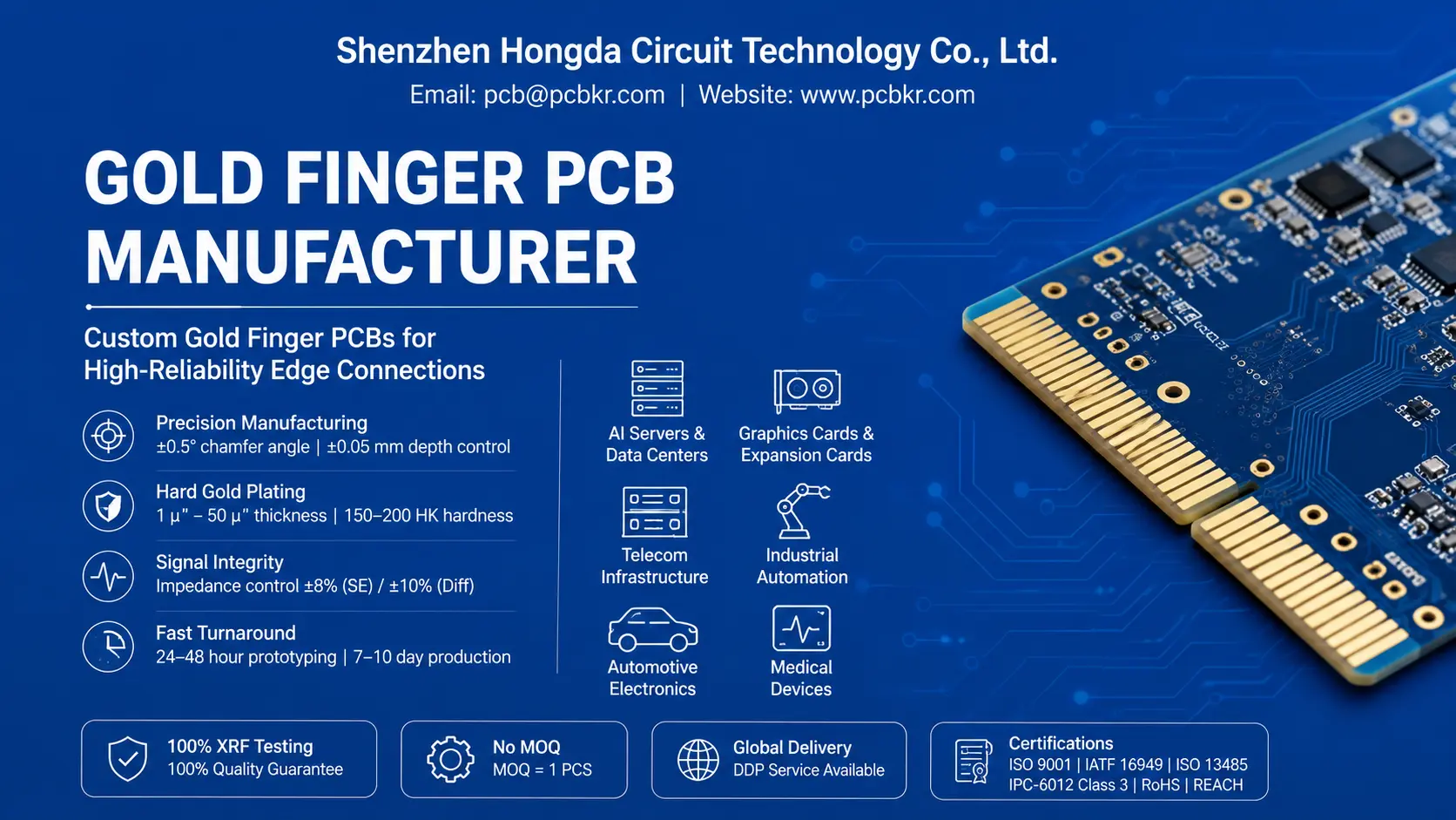
Leading China Gold Finger PCB Manufacturer & Custom Factory
High-Precision Hard/Soft Gold Finger PCBs from Rapid Prototyping to High-Volume Production
ISO 9001 | IATF 16949 | UL Certified | IPC-6012 Class 3 | 15+ Years Gold Finger Expertise
Why Partner with Us as Your Gold Finger PCB Supplier?
When sourcing gold finger PCBs, procurement teams and design engineers face four critical pain points that separate reliable suppliers from commodity fabricators. At Shenzhen Hongda Circuit Technology Co., Ltd., we have engineered our entire manufacturing workflow around solving these challenges.
Pain Point 1: Contact Instability & Premature Wear
The Problem: Gold fingers that fail after 50–100 insertion cycles, exhibiting contact resistance drift, gold flaking, or exposed nickel corrosion. This failure mode typically traces to insufficient gold thickness, improper cobalt hardener concentration, or inadequate nickel underplate hardness.
Our Solution: We strictly control gold layer thickness from 1 μ” to 50 μ” (0.025–1.27 μm) across our dual hard gold plating lines, with real-time XRF monitoring maintaining ±10% thickness uniformity. Our Umicore Auruna 3110 electrolyte deposits cobalt-hardened gold (150–180 HK Knoop hardness) over Atotech Nichem MP 2000 electrolytic nickel (450–500 HV), achieving wear life exceeding 10,000 insertion cycles for industrial and military applications.
Pain Point 2: Chamfer Precision & Insertion Force Variability
The Problem: Inconsistent bevel angles create insertion force variations that damage mating connectors, cause stubbing during hot-swap operations, or fail to provide adequate contact wipe for debris removal. Manual sanding or low-tolerance CNC machines produce ±2°–5° angular deviation—unacceptable for 0.5 mm pitch PCIe connectors.
Our Solution: Our Schmoll BZ-3000 CNC beveling station with diamond-coated V-bits achieves ±0.5° angular tolerance and ±0.05 mm depth control. We offer standard angles of 20°, 30°, 45°, and 60°, with dual-angle chamfer capability (30° primary + 15° secondary) for high-insertion-cycle applications. Every beveled edge undergoes Keyence IM-8000 optical verification before shipment.
Pain Point 3: Signal Degradation in High-Speed Designs
The Problem: As PCIe 5.0/6.0 and DDR5 push data rates beyond 32 GT/s, gold finger geometry directly impacts impedance continuity. Inconsistent finger width, pitch variation, or chamfer-induced impedance discontinuities cause signal reflection, eye closure, and bit errors.
Our Solution: Our Orbotech Nuvogo 1000 LDI system exposes finger patterns at ±5 μm registration accuracy, maintaining single-ended impedance within ±8% and differential impedance within ±10%. For AI server customers, we perform TDR (Time Domain Reflectometry) testing on gold finger interfaces to verify impedance continuity from trace to connector transition.
Pain Point 4: MOQ Barriers & Prototype Lead Times
The Problem: Many gold finger PCB manufacturers impose 100+ panel MOQs and 3-week lead times, blocking R&D teams from rapid design iteration. Shared plating lines prioritize high-volume orders, relegating prototypes to inconsistent quality.
Our Solution: No Minimum Order Quantity (MOQ = 1 PCS). Our dedicated prototype cell processes gold finger boards in 24–48 hours for first-article validation, with production ramp to 5,000+ panels/week through automated lines. Every order—whether 1 panel or 10,000—receives identical process control and 100% XRF thickness verification.
Advanced Gold Finger PCB Manufacturing Capabilities
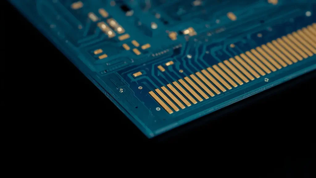
High-Precision Custom Gold Finger PCB with 45° Beveled Edge
| Specification | Hongda Circuit Capability | Industry Typical | Competitive Advantage |
|---|---|---|---|
| Gold Finger Types | Hard Gold, ENIG, ENEPIG, Segmented Gold Fingers, Long-Short Fingers | Hard Gold, ENIG only | Full selective finish portfolio |
| Gold Thickness Range | 1 μ” – 50 μ” (0.025–1.27 μm) | 10 μ” – 30 μ” | Ultra-thin to military-heavy gold |
| Gold Hardness (Knoop) | 130–200 HK | 130–180 HK | Cobalt optimization for wear life |
| Beveling Angles | 20°, 30°, 45°, 60°, dual-angle | 30°, 45° only | Custom angles for any connector |
| Bevel Tolerance | ±0.5° angle, ±0.05 mm depth | ±2° angle | Prevents connector damage |
| Board Thickness | 0.4 mm – 3.2 mm (±10%) | 0.8 mm – 2.4 mm | Ultra-thin to heavy copper |
| Pitch (Center-to-Center) | 0.5 mm – 2.54 mm | 1.0 mm – 2.54 mm | High-density 0.5 mm PCIe/M.2 |
| Pitch Tolerance | ±0.025 mm | ±0.05 mm | Critical for 0.5 mm connectors |
| Impedance Control | Single-ended ±8%, Differential ±10% | ±10% / ±15% | PCIe 5.0/6.0 signal integrity |
| Finger Length | Up to 40 mm | Up to 30 mm | Extended contact for power fingers |
| Nickel Underplate | 3.8–7.6 μm (150–300 μin) | 3.0–5.0 μm | Enhanced diffusion barrier |
| Nickel Hardness | 450–500 HV | 400–450 HV | Superior wear support |
| Maximum Panel Size | 610 mm × 457 mm (24” × 18”) | 508 mm × 406 mm | Larger panels = lower unit cost |
| Layer Count | 2–32 layers | 2–16 layers | Complex backplanes and servers |
| Copper Weight (Fingers) | 1 oz – 4 oz (35–140 μm) | 1 oz – 2 oz | High-current power distribution |
| Testing Coverage | 100% AOI, 100% XRF, 100% Electrical | 100% AOI, spot XRF | Zero-defect shipment guarantee |
| Prototype Lead Time | 24–48 hours (expedite) | 5–7 days | Fastest R&D validation |
| Production Lead Time | 7–10 days standard | 12–15 days | Compressed supply chain |
| Monthly Capacity | 50,000 m² | 20,000 m² | Scale for high-volume programs |
Our Gold Finger PCB Equipment & Technology Stack
Hard Gold Plating Lines (2 Dedicated Lines)
| Equipment | Model | Specification | Purpose |
|---|---|---|---|
| Electrolytic Nickel Plating | Atotech Nichem MP 2000 | 4.5–6.0 μm Ni, 450–500 HV | Diffusion barrier, mechanical support |
| Hard Gold Electroplating | Umicore Auruna 3110 | Co-hardened, 150–180 HK | Wear-resistant contact surface |
| Real-Time Thickness Monitor | Fischer XDV-SDD XRF | ±5% accuracy, 50 μm spot | 100% finger verification |
| Pulse Plating Controller | Atotech InPulse 2 | 1–10 Hz frequency, 10–90% duty | Uniform throwing power |
| Bath Chemistry Analyzer | Metrohm 930 Compact IC | pH, metal ion, additive concentration | Automated chemistry control |
Process Innovation: Our pulse-reverse pulse (PRP) plating technology—adapted from our HDI microvia production—applies periodic current reversal during gold deposition. This refines grain size from 2 μm (DC plating) to <0.5 μm (PRP), increasing gold hardness by 15% and extending wear life by 30% compared to conventional DC hard gold.
Selective Plating & Masking Systems
| Equipment | Model | Capability |
|---|---|---|
| LDI Exposure | Orbotech Paragon-X | ±8 μm registration, 25 μm line/space |
| Dry Film Laminator | Tamarack 6200 | 25–50 μm photoresist, vacuum lamination |
| Photoresist Developer | Schmid ECO Developer | Alkaline develop, 0.5 μm resolution |
| Blue Glue Masking | Manual + Semi-auto | Cost-effective for prototype/low-volume |
Selective vs. Full-Edge Plating: We offer both approaches. Selective plating (photoresist masking) reduces gold consumption by 60–80% and is standard for cost-sensitive applications. Full-edge plating (tape masking) ensures complete edge coverage for boards with fingers on multiple edges or irregular geometries. Our engineers recommend the optimal approach based on your design and volume.
Precision Chamfering & Profiling
| Equipment | Model | Specification |
|---|---|---|
| CNC Beveling Machine | Schmoll BZ-3000 | 30,000 RPM spindle, diamond V-bits |
| Angle Verification | Keyence IM-8000 | ±0.1° optical measurement |
| Edge Profile Router | Schmoll MX-500 | ±0.025 mm routing tolerance |
| Surface Roughness Gauge | Mitutoyo SJ-210 | Ra <0.4 μm verification |
Dual-Angle Chamfer Technology: For hot-swap server modules requiring low insertion force (<0.8 N/finger) and adequate contact wipe, our dual-angle chamfer combines a 30° primary angle for insertion guidance with a 15° secondary angle for progressive contact engagement. This reduces peak insertion force by 40% compared to single-angle chamfers while maintaining reliable electrical contact.
Quality Assurance & Testing Laboratory
| Equipment | Model | Test Application |
|---|---|---|
| AOI System | Orbotech Discovery 8800 | 100% finger surface defect detection |
| XRF Thickness Gauge | Fischer XDV-SDD | Gold/nickel thickness, 5 points/finger |
| Contact Resistance Tester | Custom 4-wire probe | <20 mΩ per finger, 100% sampling |
| Insertion Force Gauge | Mecmesin MultiTest | 0.1–50 N force measurement |
| Wear Cycle Simulator | Custom test fixture | 1–10,000 cycle automated insertion |
| Microsection System | Buehler EcoMet 30 | Cross-section analysis, grain structure |
| SEM/EDX Analyzer | Hitachi SU3500 | Failure analysis, contamination detection |
| Salt Spray Chamber | Q-FOG CCT-1100 | 96–1,000 hr corrosion testing |
| TDR Analyzer | Keysight N1000A | Impedance continuity for high-speed designs |
Original Factory Direct: From Rapid Prototyping to High-Volume Production
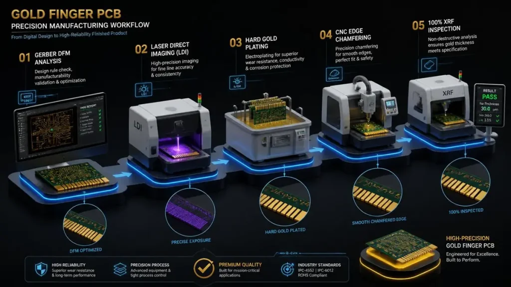
Gold Finger PCB Precision Manufacturing Workflow Infographic | Shenzhen Hongda Circuit Technology
No Middlemen. No Markup. Direct Engineering Access.
As a factory-direct gold finger PCB manufacturer, Shenzhen Hongda Circuit eliminates distributor margins and communication delays. When you contact us, you speak directly with the engineers who will build your boards—not a sales broker who forwards requirements overseas.
Rapid Prototyping: 24–48 Hour First Articles
Our dedicated prototype cell operates independently from high-volume production, ensuring your development boards receive priority processing without disrupting mass production schedules:
| Prototype Service | Standard Lead Time | Expedite Lead Time | MOQ |
|---|---|---|---|
| Gold Finger Prototype (1–10 panels) | 3–5 days | 24–48 hours | 1 panel |
| First Article with XRF Report | 5 days | 3 days | 1 panel |
| Engineering Validation (10–50 panels) | 7 days | 5 days | 5 panels |
| Pre-Production Qualification (50–200 panels) | 10 days | 7 days | 50 panels |
DFM Review Included: Every prototype order includes a complimentary Design for Manufacturing (DFM) review by our gold finger specialists. We verify:
- Chamfer angle compatibility with your connector specification
- Finger pitch tolerance against connector datasheet
- Inner layer copper pull-back compliance (0.6 mm minimum for 1.6 mm boards)
- Gold thickness recommendation based on insertion cycle requirements
- Solder mask keepout zone adequacy (0.5 mm minimum)
High-Volume Production: Automated Lines, Consistent Quality
For production volumes exceeding 200 panels, our automated hard gold plating lines deliver: • Throughput: 500 panels/day across 2 plating lines • Consistency: Cpk >1.67 for gold thickness, Cpk >1.33 for chamfer angle • Traceability: Panel-level barcode tracking from raw material to shipment • Kanban/VMI Support: Blanket orders with scheduled releases to optimize inventory
Custom Gold Finger PCB: If You Can Design It, We Can Build It
| Custom Feature | Capability | Typical Application |
|---|---|---|
| Segmented Gold Fingers | Interrupted contact zones with insulating gaps | Specialized signaling interfaces |
| Long-Short Fingers | Uneven length for power sequencing (power-before-data) | Hot-swap server modules, USB flash drives |
| Multiple Edge Fingers | Fingers on 2–4 board edges | Compact embedded systems |
| Non-Standard Pitch | 0.3 mm – 3.0 mm custom pitch | Proprietary connector systems |
| Thick Copper Fingers | 3 oz – 4 oz (105–140 μm) copper | High-current power distribution |
| Fingers with Cutouts/Slots | Notched fingers for polarization/keying | Prevent incorrect insertion |
| Selective Finish Combination | Hard gold fingers + ENIG pads + OSP holes | Mixed-technology boards |
| Flexible Gold Fingers | Polyimide substrate with gold contacts | Wearable devices, medical sensors |
Strict Quality Control & Global Industry Certifications
Quality Management System
Our quality system is built on IPC-A-600 Class 2/Class 3 visual acceptance criteria and IPC-6012F performance specifications, with additional industry-specific overlays:
| Certification | Standard | Scope | Gold Finger Relevance |
|---|---|---|---|
| ISO 9001:2015 | Quality Management | Company-wide | Process control, continuous improvement |
| IATF 16949:2016 | Automotive Quality | Automotive product line | PPAP, SPC, zero-defect culture |
| ISO 13485:2016 | Medical Device Quality | Medical product line | Traceability, risk management, biocompatibility |
| IPC-6012 Class 3 | High-Performance PCBs | All product lines | 100% XRF, microsection, thermal cycling |
| IPC-A-610 Class 3 | Assembly Acceptability | Post-assembly inspection | No solder contamination on gold |
| UL 94V-0 | Flammability | All laminates | Safety compliance |
| RoHS 3 (2011/65/EU) | Hazardous Substances | All products | Lead-free, cadmium-free gold plating |
| REACH (EC 1907/2006) | Chemical Registration | All products | SVHC disclosure, cobalt salt management |
| MIL-PRF-31032 | Military PCBs | Military product line | 5.08 μm gold, 10,000 cycle qualification |
Gold Finger-Specific Quality Inspection Protocol
| Inspection Stage | Method | Criteria | Frequency |
|---|---|---|---|
| Incoming Material | Copper foil resistivity, laminate Tg verification | Per IPC-4101 | Every lot |
| Inner Layer Etching | AOI (Orbotech Discovery) | No open/short, width ±10% | 100% panels |
| Nickel Plating | XRF thickness, Hull cell test | 4.5–6.0 μm, adhesion pass | Every 2 hours |
| Gold Plating | XRF thickness (5 points/finger) | ±10% of spec | 100% fingers |
| Gold Hardness | Knoop microhardness tester | 150–180 HK | Daily sample |
| Chamfering | Optical angle gauge, profile projector | ±0.5° angle, ±0.05 mm depth | 100% edges |
| Adhesion | 3M 600 tape test (IPC-TM-650 2.4.28) | No gold transfer to tape | AQL 1.0 |
| Contact Resistance | 4-wire Kelvin measurement | <20 mΩ per finger | 100% sampling |
| Visual Inspection | 10× stereo microscope | No pits, nodules, discoloration | 100% panels |
| Final Electrical | Flying probe or ICT | Opens, shorts, netlist verification | 100% boards |
| Microsection (FA) | Cross-section, SEM/EDX | Grain structure, interface quality | First article + monthly |
| Wear Testing (FA) | Automated insertion/removal | <10% resistance change at target cycles | Qualification only |
Flexible Order Terms, Fast Lead Times & Clear Production Roadmap
Order Quantity & Pricing Structure
| Order Tier | Quantity | Price Advantage | Lead Time | Best For |
|---|---|---|---|---|
| Prototype | 1–10 panels | Base price | 3–5 days (24–48 hr expedite) | R&D validation, proof-of-concept |
| Small Batch | 11–100 panels | 5% volume discount | 7–10 days | Pilot production, beta testing |
| Medium Batch | 101–500 panels | 12% volume discount | 10–12 days | Market launch, initial deployment |
| High Volume | 501–2,000 panels | 20% volume discount | 12–15 days | Full production, supply chain |
| Mass Production | 2,000+ panels | Custom negotiated | 15–20 days | OEM programs, annual contracts |
Lead Time Breakdown by Process Stage
| Stage | Standard | Expedite | Notes |
|---|---|---|---|
| DFM Review & Quote | 4–8 hours | 2–4 hours | Free for all orders |
| Material Procurement | 1–2 days | 1 day | Stocked laminates: FR-4, High Tg, Rogers |
| Fabrication (Etching/Lamination) | 2–3 days | 1–2 days | LDI exposure eliminates film delays |
| Nickel/Gold Plating | 1–2 days | 1 day | Dedicated lines, no queue waiting |
| Chamfering & Routing | 0.5–1 day | 0.5 day | CNC automation, minimal setup |
| Testing & Inspection | 0.5–1 day | 0.5 day | Parallel processing |
| Packaging & Shipment | 0.5 day | 0.5 day | ESD vacuum packaging |
| Total Standard | 7–10 days | 5–7 days | From Gerber approval to dispatch |
| Total Prototype | 3–5 days | 24–48 hours | Dedicated prototype cell |
Shipping & Logistics
| Destination | Shipping Method | Transit Time | Cost Structure |
|---|---|---|---|
| Asia (Local) | Truck/Express | 1–3 days | Included for orders >$500 |
| Europe | DHL/FedEx Express | 3–5 days | DDP (Delivered Duty Paid) available |
| North America | DHL/FedEx Express | 4–6 days | DDP available |
| Global | Air Freight | 5–8 days | FOB Shenzhen or CIF destination |
| High Volume | Sea Freight | 15–30 days | Most economical for >500 kg |
Our Step-by-Step Manufacturing Journey: Transparent Process Control
Step 1: DFM Review & Engineering Validation (0–8 Hours)
Before production begins, our gold finger engineering team performs a comprehensive Design for Manufacturing review: • Gerber analysis: Verify finger dimensions, pitch, and chamfer specifications against IPC-2221 • Impedance simulation: For high-speed designs, validate trace-to-finger transition continuity • Material selection: Recommend laminate (FR-4, High Tg, Rogers) based on operating environment • Gold thickness recommendation: Match thickness to insertion cycle requirements and budget • Panelization optimization: Maximize finger count per panel to reduce unit cost
Deliverable: DFM report with engineering recommendations and production approval.
Step 2: Circuit Fabrication & Precision Etching (1–3 Days)
• LDI Exposure: Orbotech Nuvogo 1000 exposes outer-layer finger patterns at ±5 μm accuracy • Etching: Horizontal conveyor etcher with real-time specific gravity control maintains ±10% width tolerance • AOI: 100% automated optical inspection catches open circuits, shorts, and width violations before plating
Step 3: Electrolytic Nickel & Hard Gold Plating (1–2 Days)
• Surface Preparation: Micro-etch (1–2 μm copper removal) + acid activation for nickel adhesion • Nickel Plating: Atotech Nichem MP 2000 deposits 4.5–6.0 μm electrolytic nickel at 450–500 HV • Selective Masking: Orbotech Paragon-X LDI defines hard gold area with ±8 μm registration • Hard Gold Deposition: Umicore Auruna 3110 deposits cobalt-hardened gold; Fischer XRF verifies thickness every 15 minutes • PRP Enhancement: Pulse-reverse pulse plating refines grain structure for 30% extended wear life
Step 4: Precision Chamfering & Edge Profiling (0.5–1 Day)
• CNC Beveling: Schmoll BZ-3000 machines chamfer at specified angle with diamond V-bit • Dual-Angle Option: Secondary pass for 15° contact wipe angle on high-cycle applications • Edge Routing: Final profile routing removes plating tie-bars and achieves ±0.025 mm dimensional tolerance • Optical Verification: Keyence IM-8000 confirms angle within ±0.5°
Step 5: Comprehensive QA Testing & Certification (0.5–1 Day)
• XRF Thickness: 100% finger coverage, 5 measurement points per finger • Contact Resistance: 4-wire Kelvin test, <20 mΩ per finger • Adhesion Tape Test: 3M 600 tape per IPC-TM-650 2.4.28 • Visual Inspection: 10× stereo microscope, 100% panels • Electrical Test: Flying probe or ICT, 100% continuity/isolation • TDR Testing: For high-speed designs, impedance verification across finger interface
Step 6: ESD-Safe Packaging & Global Delivery (0.5 Day)
• Anti-static vacuum sealing: Prevents oxidation and contamination during transit • Humidity indicator cards: Monitor moisture exposure • Custom labeling: Barcode traceability, RoHS/REACH declarations, material certificates • Documentation: C of C, IPC compliance report, XRF thickness data, microsection photos (if requested)
Key Technical Points of Custom Gold Finger PCB
What Is the Ideal Gold Thickness for PCB Gold Fingers?
The optimal PCB gold finger thickness depends entirely on your application’s insertion cycle requirement: • 1–5 μ” (0.025–0.13 μm): Prototyping, very low cycle, cost-sensitive consumer • 10–30 μ” (0.25–0.76 μm): Standard gaming cards, network cards, general expansion cards (50–200 cycles) • 30–50 μ” (0.76–1.27 μm): Industrial backplanes, AI server PCIe cards, medical devices (500–2,000 cycles) • 50–100 μ” (1.27–2.54 μm): Telecom infrastructure, automotive ECU adapters (2,000–5,000 cycles) • 100–200 μ” (2.54–5.08 μm): Military, aerospace, extreme wear test fixtures (5,000–10,000+ cycles)
At Hongda Circuit, we recommend 30 μ” (0.76 μm) as the standard for general industrial applications—balancing cost and durability. For mission-critical applications, our engineers will model wear life based on your specific insertion force, contact material, and environmental conditions.
What Is the Difference Between Hard Gold and ENIG for Gold Fingers?
This is the most critical distinction in gold finger specification:
| Attribute | Hard Gold (Electroplated) | ENIG (Immersion) |
|---|---|---|
| Thickness | 1–50 μ” (0.025–1.27 μm) | 2–5 μ” (0.05–0.13 μm) |
| Hardness | 130–200 HK (cobalt-hardened) | 50–70 HK (pure, soft) |
| Wear Life | 1,000–10,000+ cycles | 1–5 cycles |
| Contact Resistance | <20 mΩ, stable | 50–100 mΩ, degrades |
| Cost | Higher (gold consumption) | Lower (thin layer) |
| Use Case | Edge connectors, wear surfaces | Solder pads only |
Never use ENIG for gold fingers. The thin, soft immersion gold layer will gall, wear through, and expose nickel to oxidation within 1–10 insertion cycles. Hard gold is electroplated, alloyed with cobalt or nickel for hardness, and engineered specifically for mechanical wear resistance.
Why Is Edge Beveling Important for Custom Gold Finger PCBs?
PCB gold finger chamfering (beveling) serves three essential functions:
- Insertion Guidance: The angled lead-in prevents the PCB edge from “stubbing” against the connector housing, reducing insertion force by 30–50%.
- Contact Wipe: The chamfer creates progressive engagement that wipes oxide and debris from the mating contact before full electrical connection—critical for maintaining low contact resistance.
- Connector Protection: A sharp, unbeveled PCB edge can damage delicate connector contacts (gold-plated springs, beryllium copper fingers), causing permanent deformation and increased contact resistance.
Without proper beveling, insertion force increases 2–3×, accelerating wear on both the PCB gold finger and the mating connector. For hot-swap applications (server blades, industrial I/O), beveling is not optional—it is a reliability requirement.
Can You Manufacture Segmented or Uneven Length Gold Fingers?
Yes. Segmented gold fingers (interrupted contact zones with insulating gaps) and long-short fingers (uneven lengths for power sequencing) are specialties at Hongda Circuit: • Segmented Fingers: Used for specialized signaling interfaces where non-contiguous contact zones prevent crosstalk or enable multi-function pins. Our LDI masking achieves 25 μm line/space resolution for precise gap definition. • Long-Short Fingers: Critical for hot-swap designs where power pins must mate before data pins (or disconnect after). Typical configurations: power fingers 2.0 mm longer than data fingers, ensuring 50 ms power stabilization before signal engagement. • Fingers with Cutouts/Keying: Notched fingers prevent incorrect insertion orientation. Our CNC routing achieves ±0.025 mm notch tolerance.
How Do I Verify a Gold Finger PCB Manufacturer’s True Capability?
Use this 5-point audit checklist when evaluating gold finger PCB suppliers:
- Verify Dedicated Hard Gold Equipment [ ] Dedicated hard gold plating line (not shared with ENIG/HASL) [ ] Real-time XRF thickness monitoring (not spot-check) [ ] Cobalt-hardened gold chemistry (not pure soft gold)
- Inspect Chamfering Capability [ ] CNC beveling machine (not manual sanding) [ ] Angle verification with optical gauge (not visual estimation) [ ] Dual-angle capability for high-cycle applications
- Review Quality Documentation [ ] XRF thickness report for every production lot [ ] Contact resistance test data (<20 mΩ) [ ] Adhesion tape test results (IPC-TM-650) [ ] Microsection photos showing nickel/gold interface
- Validate Industry Experience [ ] Customer references in your target industry (AI server, automotive, medical) [ ] Qualification test reports (thermal cycling, wear cycling) [ ] IPC-6012 Class 3 certification (not just Class 2)
- Assess Engineering Support [ ] Free DFM review with gold finger-specific recommendations [ ] Application engineer familiar with your connector specification [ ] Rapid prototype capability (24–48 hour turnaround)
At Hongda Circuit, we welcome virtual factory tours and provide full transparency into our equipment, process parameters, and quality data. Our Customer Quality Portal grants real-time access to inspection reports, XRF data, and process SPC charts for every order.
Ready to Start Your Gold Finger PCB Project?
Whether you need a single prototype for R&D validation or a 10,000-panel annual contract, Shenzhen Hongda Circuit Technology Co., Ltd. delivers gold finger PCBs with the precision, reliability, and speed your project demands.
Get Started in Three Steps:
Step 1: Upload your Gerber files and specifications Step 2: Receive DFM review and quote within 4–8 hours Step 3: Approve production and track progress in real time
What You’ll Receive:
✓ Free DFM Review — Gold finger-specific engineering recommendations ✓ Competitive Quote — Transparent pricing, no hidden fees ✓ Fast Prototyping — 24–48 hour first articles available ✓ 100% Quality Guarantee — XRF verified, AOI inspected, electrically tested ✓ Global Shipping — DDP delivery to your door
Shenzhen Hongda Circuit Technology Co., Ltd. Building 3, Hongda Industrial Park, Bao’an District, Shenzhen, China 518104 Email: sales@pcbkr.com
FAQ
What is your standard lead time for custom Gold Finger PCBs, and can you handle expedited urgent orders?
Our standard lead time for prototype Gold Finger PCBs is 3–5 working days, with mass production taking 7–10 working days depending on panel volume and gold plating thickness. For urgent project deadlines, we offer an expedited 24–48 hour fast-turn service for first-article prototypes. All expedited orders receive dedicated line scheduling to guarantee on-time delivery without compromising quality inspection.
What is your Minimum Order Quantity (MOQ) and price structure for prototype vs. mass production?
We have No Minimum Order Quantity (MOQ = 1 PCS) for prototype and engineering validation boards. We offer transparent tier-based volume pricing: prototype runs are billed at standard base rates, while small-to-medium production runs (11–500 panels) receive a 5%–12% discount, and mass production orders (>500 panels) benefit from up to 20%+ volume discounts with custom-negotiated annual contracts.
How do you ensure quality compliance and traceability for international B2B shipments?
Every production batch undergoes 100% XRF gold thickness testing, 100% AOI inspection, and 100% electrical flying probe testing. We are certified under ISO 9001:2015, IATF 16949 (Automotive), and UL (E-file), conforming to IPC-6012 Class 3 standards. Each shipment includes a comprehensive documentation package: Certificate of Conformity (C of C), IPC Test Report, XRF Thickness Inspection Data, and RoHS/REACH Compliance Certificates. Panel-level barcode tracking ensures complete raw material and process traceability.
What trade and shipping terms (incoterms) do you support for overseas buyers?
We support flexible international trade terms including EXW, FOB Shenzhen, CIF, and DDP (Delivered Duty Paid). For customers in North America and Europe using our DDP service, we handle all export/import clearance, customs duties, and taxes directly, delivering goods seamlessly to your facility via DHL, FedEx, or air freight.
Can you provide a free DFM review and instant quote before we place a formal order?
Yes, absolutely. We provide a 100% Free Design for Manufacturing (DFM) review for all Gerber files within 4 to 8 hours. Our gold finger engineering team will analyze your Gerber data, verify finger pitch, check chamfer angle tolerances, and review inner-layer copper pull-backs to prevent manufacturing defects before you spend a single dollar.
About Author
David Chen https://www.linkedin.com/in/pcbcoming
David Chen boasts an extensive professional background in PCBA manufacturing, PCBA testing, and PCBA optimization, with specialized expertise in high-precision PCBA fault analysis and rigorous PCBA reliability testing. The author has worked with high-layer-count server PCB fabrication, ultra-low-loss backplane stackups, and thermo-mechanical reliability optimization for AI infrastructure projects involving 112G and 224G PAM4 architectures. Skilled in complex circuit design and cutting-edge advanced PCB manufacturing processes, he delivers solutions that elevate product durability and performance across industrial applications. His technical articles focusing on PCBA manufacturing workflows and testing methodologies are widely cited by industry peers, research institutions, and technical platforms, solidifying his reputation as a recognized technical authority in the global circuit board manufacturing sector.