How to Make Glass Epoxy PCB: Manufacturing Process Guide
A glass epoxy PCB is manufactured by combining woven glass reinforcement, epoxy resin, and copper through controlled imaging, etching, multilayer lay‑up, vacuum lamination, drilling, desmear, copper plating, solder mask, surface finishing, and electrical inspection. The critical manufacturing challenge is controlling how glass and resin behave together throughout the process.
How Is a Glass Epoxy PCB Manufactured From Raw Material to Finished Board?
A glass epoxy PCB typically follows this manufacturing sequence: material preparation, inner‑layer imaging, etching, AOI, multilayer lay‑up, lamination, drilling, desmear, copper metallization, outer‑layer imaging and plating, solder mask, surface finish, electrical testing, profiling, and final inspection.
The process is not simply a sequence of chemical and mechanical operations. Each operation changes the dimensional, thermal, mechanical, or electrical condition of the composite board.
A typical multilayer glass epoxy PCB manufacturing flow is: Material Selection → Inner‑Layer Imaging → Etching → AOI → Lay‑Up → Lamination → Drilling → Desmear → Electroless Copper → Electroplating → Outer‑Layer Imaging → Etching → Solder Mask → Surface Finish → Electrical Test → Final Inspection
FR‑4 is one of the most widely used glass‑fiber‑reinforced epoxy PCB material systems, but FR‑4 should not be treated as one single laminate formulation. Glass style, resin content, copper foil, dielectric thickness, resin chemistry, and laminate supplier can all change manufacturing behavior.
For procurement engineers, this distinction matters because two boards both specified as “FR‑4” can require different manufacturing controls.
How Does Glass and Resin Composition Affect Glass Epoxy PCB Manufacturing?
Glass reinforcement provides mechanical structure and dimensional stability, while epoxy resin provides bonding, insulation, resin flow, and dielectric filling during lamination. Manufacturing quality depends on controlling the interaction between these two materials.
A glass epoxy PCB is a composite structure rather than a homogeneous material.
The glass bundles do not behave like the surrounding resin during drilling, heating, or dimensional movement. During lamination, the resin softens and flows while the glass reinforcement retains much more of its structural function.
This creates three important manufacturing variables:
| Material element | Manufacturing function | Typical risk |
|---|---|---|
| Glass fiber | Reinforcement and dimensional stability | Fiber pullout, drilling resistance |
| Epoxy resin | Bonding and dielectric insulation | Voids, resin starvation, smear |
| Copper | Electrical conductor | Etch variation, plating variation |
How Does Glass Reinforcement Affect Dimensional Stability?
Glass reinforcement helps limit dimensional movement, but it does not eliminate it.
During inner‑layer fabrication, lamination, cooling, drilling, and subsequent thermal processing, the panel can experience X‑Y dimensional changes. The amount depends on laminate construction, copper distribution, glass style, resin system, temperature history, moisture condition, and panel geometry.
This is why multilayer PCB manufacturing requires dimensional compensation rather than assuming that a nominal CAD dimension will remain unchanged after every process.
For high‑density boards, registration errors can become especially important around:
- Fine‑pitch BGA land patterns
- Microvia structures
- Backdrilled vias
- Differential‑pair geometries
- Small annular rings
- High layer‑count stackups
A manufacturer therefore needs process‑specific registration control rather than simply checking the finished board.
How Does Resin Distribution Affect Multilayer PCB Manufacturing?
Resin distribution directly influences dielectric thickness, bonding, copper‑to‑laminate adhesion, and multilayer dimensional behavior.
During lamination, prepreg resin must flow sufficiently to fill the spaces created by copper patterns and bond adjacent layers. Too little effective resin flow can contribute to resin‑starved areas or incomplete bonding. Excessive flow can change dielectric thickness and create local resin‑rich regions.
Copper pattern density is therefore part of the lamination problem.
A dense copper area and a large resin‑rich area do not respond identically during pressing. For demanding multilayer designs, stackup engineering should consider copper distribution, prepreg selection, target dielectric thickness, and the required final impedance.
How Does Inner‑Layer Imaging and Etching Work in Glass Epoxy PCB Fabrication?
Inner‑layer copper is cleaned, coated with photoresist, imaged, developed, etched, stripped, and inspected before the layers are assembled into the multilayer structure.
The manufacturing engineer begins with copper‑clad laminate or an appropriate inner‑layer core.
The circuit image is transferred onto the copper surface using the selected imaging process. After development, exposed copper is chemically removed to create the required circuit geometry.
The critical issue is not merely whether the trace exists. It is whether the finished conductor has the required width, spacing, registration, and copper integrity.
How Is Inner‑Layer Registration Controlled?
Registration is controlled through a combination of imaging accuracy, panel compensation, tooling, material conditioning, and inspection.
For conventional boards, moderate dimensional variation may have little practical effect. On high‑density multilayer PCBs, the same movement can reduce annular‑ring margins or create via‑to‑pad misalignment.
Modern PCB factories increasingly use LDI and automated inspection to reduce dependence on conventional artwork alignment methods.
For procurement, the important question is not simply:
“Can you manufacture fine lines?”
A better question is:
“What registration capability is maintained through imaging, lamination, drilling, and final inspection?”
That question evaluates the complete manufacturing chain.
How Is Multilayer Glass Epoxy PCB Lay‑Up Prepared?
Finished inner layers, prepreg, and copper foil are stacked according to the approved stackup, with each dielectric layer selected to achieve the required thickness and bonding performance.
A typical multilayer construction may contain: Copper Foil → Prepreg → Inner‑Layer Core → Prepreg → Inner‑Layer Core → Prepreg → Copper Foil
The actual configuration depends on layer count and electrical requirements.
Before lay‑up, inner layers are normally inspected and the copper surface is prepared to promote reliable bonding. Oxide or alternative surface treatments can increase the effective bonding interface between copper and resin.
The lay‑up sequence must control:
- Layer order
- Prepreg type
- Resin content
- Core thickness
- Copper thickness
- Lamination symmetry
- Tooling and registration
- Copper pattern distribution
For a high‑layer‑count board, one incorrect prepreg or core position can affect both total thickness and electrical performance.
How Does Lamination Affect Glass Epoxy PCB Manufacturing?
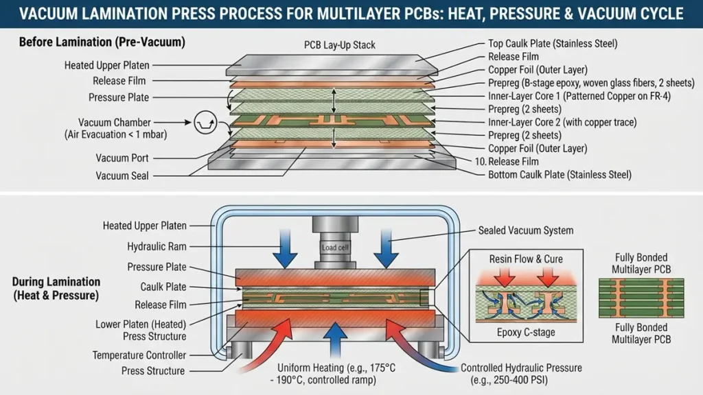
Vacuum lamination binds inner-layer cores, prepreg, and copper foils together under strict temperature and pressure profiles to form a solid multilayer glass epoxy PCB.
Lamination transforms separately processed cores, prepreg, and copper foils into one multilayer structure by applying a controlled temperature, pressure, vacuum, and time profile.
Lamination is one of the most important steps in glass epoxy PCB manufacturing because it determines whether the internal structure becomes a mechanically stable and electrically reliable laminate.
During the press cycle, epoxy resin softens and flows before curing. The process must allow the resin to wet the relevant surfaces and fill the required spaces without creating unacceptable voids or dimensional distortion.
Commercial PCB processes commonly use vacuum‑assisted hot pressing, but the exact temperature and pressure profile must be qualified for the selected laminate system rather than copied from another material.
How Does Resin Flow During FR4 PCB Lamination?
Resin flow is influenced by:
- Prepreg resin content
- Glass style
- Resin viscosity
- Copper pattern density
- Lamination temperature
- Pressure profile
- Heating rate
- Vacuum condition
- Cure characteristics
The engineering objective is not “maximum resin flow.” The objective is controlled resin flow.
If resin flow is insufficient, bonding and filling can become problematic. If flow is excessive, dielectric thickness can shift and resin may be displaced from areas where adequate insulation is required.
What Causes Voids and Resin Starvation During Lamination?
Common contributors include unsuitable prepreg selection, trapped air, excessive copper density, contamination, inadequate vacuum, improper press parameters, or poor material conditioning.
Resin starvation is particularly important because a visually acceptable board may still contain a locally unfavorable resin distribution.
For high‑reliability multilayer PCBs, microsection analysis can verify the internal laminate structure rather than relying only on external appearance.
How Does Glass Fiber Affect Glass Epoxy PCB Drilling?
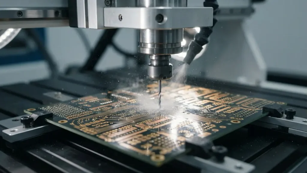
CNC Drilling Process for Glass Epoxy PCB Manufacturing
Glass fiber and epoxy have different mechanical responses during drilling, so tool condition, drilling parameters, stack construction, hole geometry, and support conditions must be controlled together.
Mechanical drilling creates holes through alternating regions of copper, epoxy, and glass reinforcement.
This heterogeneous structure explains why drilling FR‑4 is not equivalent to drilling a homogeneous plastic.
Typical drilling problems include:
- Resin smear
- Glass‑fiber pullout
- Burr formation
- Hole‑wall roughness
- Hole‑position error
- Delamination
- Drill wear
- Oversized or undersized holes
Drill selection and process parameters should therefore be qualified against the actual laminate construction and required aspect ratio.
How Are Drill Smear, Burrs and Glass‑Fiber Pullout Controlled?
Drill smear occurs when heat and mechanical action soften or redistribute resin along the hole wall.
The problem is important because residual resin can interfere with subsequent copper metallization.
Manufacturers control the risk through tool selection, spindle and feed optimization, entry/backup materials, drill‑life management, panel construction, and post‑drilling cleaning.
Glass‑fiber pullout requires similar attention. Excessive mechanical stress can damage the hole wall or create localized irregularities that later affect plating reliability.
For demanding multilayer boards, the finished hole should be evaluated by cross‑section rather than judged only by visual inspection.
When Is Laser Drilling Used in Glass Epoxy PCB Manufacturing?
Laser drilling is commonly used when the design requires microvias or other small controlled interconnect structures that are impractical or inefficient with conventional mechanical drilling.
The laser process must account for the different absorption and removal behavior of resin and glass reinforcement.
For HDI applications, laser‑drilled microvias are typically integrated with sequential lamination, fine‑line imaging, and controlled copper filling.
The correct question for procurement is therefore not simply whether a supplier owns a laser drill. It is whether the supplier can control: Laser drilling → target registration → hole geometry → desmear → copper fill → reliability as one qualified process chain.
Why Is Desmear Important in Glass Epoxy PCB Fabrication?
Desmear removes or modifies resin residues created during drilling and prepares the hole wall for reliable copper metallization.
After drilling, the hole wall may contain resin residue, altered resin, or other contamination.
The desmear process must create a surface suitable for subsequent chemical activation and copper deposition without damaging the glass reinforcement or creating an unfavorable hole‑wall condition.
Depending on the PCB structure and material system, the manufacturing sequence may involve chemical treatment, plasma treatment, or other qualified processes.
The process window must be controlled carefully because insufficient treatment can leave residue, while excessive treatment can attack the laminate structure.
How Is Copper Plating Applied to Glass Epoxy PCB Hole Walls?
Electroless copper first establishes conductive coverage on the nonconductive hole wall, after which electroplating builds the required copper thickness.
A drilled FR‑4 hole is not electrically conductive simply because it passes through copper layers.
The exposed glass/epoxy hole wall must first be activated and metallized.
Electroless copper creates a thin conductive layer over the hole wall and panel surface. Subsequent electroplating increases copper thickness and supports the required electrical and mechanical reliability.
The critical controls include:
- Hole‑wall cleanliness
- Chemical activation
- Copper coverage
- Plating uniformity
- Current distribution
- Through‑hole copper thickness
- Surface copper thickness
- Via reliability
For demanding boards, microsection inspection can verify plated‑hole copper thickness and identify potential defects such as voids, cracks, or inadequate coverage.
How Are Outer Layers, Solder Mask and Surface Finish Manufactured?
After hole metallization, the outer circuit pattern is imaged and etched or plated according to the selected process, followed by solder mask application, surface finishing, profiling, and marking.
Outer‑layer processing must maintain the relationship between: Circuit geometry + plated copper + drilled holes + solder pads
Fine‑pitch components make registration particularly important.
Solder mask is then applied to protect exposed copper and reduce the risk of solder bridging. The selected surface finish—such as ENIG, immersion tin, OSP, or HASL—must match the assembly process and product reliability requirements.
Surface finish selection should not be treated as a cosmetic choice. It can affect solderability, flatness, shelf life, contact performance, and assembly yield.
How Is a Glass Epoxy PCB Electrically Tested and Inspected?
A production PCB should be verified through dimensional inspection, AOI, electrical testing, and—when required—X‑ray, microsection, impedance, or reliability testing.
Different inspection methods detect different defect classes.
| Inspection method | Primary purpose |
|---|---|
| AOI | Opens, shorts, pattern and solder‑mask‑related visual defects |
| X‑ray | Hidden registration and internal structural inspection |
| Electrical test | Opens and shorts |
| Microsection | Internal copper, dielectric and plated‑hole structure |
| Impedance testing | Controlled‑impedance verification |
| Dimensional inspection | Board profile and critical dimensions |
| Visual inspection | Surface and workmanship verification |
No single inspection method proves complete PCB quality.
A robust quality system matches each inspection method to the failure mechanism it is intended to detect.
What Are the Most Common Glass Epoxy PCB Manufacturing Defects?
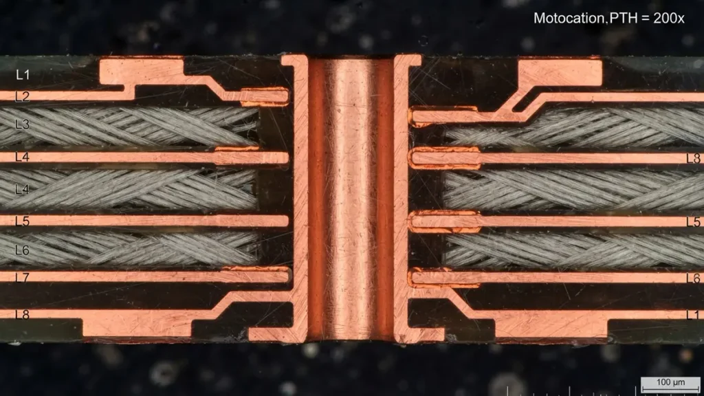
Microsection Inspection of Multilayer Glass Epoxy PCB
The most significant defects generally occur when material behavior, dimensional movement, drilling, lamination, or metallization is not adequately controlled.
| Manufacturing stage | Typical defect | Engineering concern |
|---|---|---|
| Material preparation | Moisture or material variation | Lamination/reliability |
| Imaging | Registration error | Pad and trace alignment |
| Etching | Undercut or over‑etch | Trace geometry |
| Lay‑up | Stackup error | Thickness and impedance |
| Lamination | Void | Mechanical/electrical reliability |
| Lamination | Resin starvation | Bonding and dielectric structure |
| Drilling | Burr/smear | Plating reliability |
| Drilling | Glass pullout | Hole‑wall quality |
| Desmear | Residual resin | Copper adhesion |
| Plating | Incomplete hole coverage | Electrical continuity |
| Outer layer | Pattern variation | Assembly yield |
| Solder mask | Registration error | Pad exposure |
| Surface finish | Poor coverage | Solderability |
| Final test | Open/short | Electrical failure |
The important manufacturing lesson is that many defects originate upstream.
For example, a plating failure may actually begin with poor drilling or inadequate desmear. A final registration problem may originate from material movement during lamination.
How Does Shenzhen Hongda Control Glass Epoxy PCB Manufacturing Quality?
Shenzhen Hongda Circuit Technology Co., Ltd. combines PCB engineering review, controlled multilayer processing, precision imaging, drilling, plating, AOI, X‑ray, electrical testing, and final inspection according to the board’s construction and customer requirements.
For advanced PCB manufacturing, equipment capability must be connected to a defined quality objective.
For example: LDI → imaging and registration control Laser drilling → microvia geometry and positional accuracy X‑ray → internal registration and hidden‑structure verification 3D AOI → surface and assembly‑related inspection Electrical testing → open/short screening Microsection → internal process verification
Hongda’s published manufacturing capabilities include advanced LDI, laser drilling, mSAP‑related fine‑line processing, AOI/X‑ray inspection, and equipment used for high‑density and high‑speed PCB applications.
The practical advantage is not a particular machine name. It is the ability to connect equipment, process parameters, inspection criteria, and engineering feedback into one manufacturing system.
What Should Buyers Specify When Ordering a Glass Epoxy PCB?
A serious glass epoxy PCB RFQ should specify the laminate construction, layer count, thickness, copper weight, glass/resin system, circuit geometry, hole structure, surface finish, testing, reliability class, quantity, and required delivery schedule.
A procurement RFQ should include at least:
| RFQ requirement | What to specify |
|---|---|
| PCB type | Single, double or multilayer |
| Layer count | Total copper layers |
| Finished thickness | Nominal and tolerance |
| Copper | Inner/outer copper weight |
| Material | FR‑4 or specified laminate family |
| Glass construction | Core/prepreg construction where relevant |
| Tg / thermal requirement | Based on application |
| Line/space | Minimum finished geometry |
| Hole size | Finished and/or drill diameter |
| Aspect ratio | Required hole‑depth capability |
| Impedance | Controlled values and tolerance |
| Surface finish | ENIG, HASL, OSP, immersion tin, etc. |
| Solder mask | Color and registration requirement |
| Testing | E‑test, AOI, X‑ray, microsection, impedance |
| Quality standard | IPC class/customer specification |
| Quantity | Prototype, small batch or production |
| Delivery | Required lead time |
This information lets the manufacturer evaluate manufacturability before quoting instead of discovering major process risks after order placement.
How Do You Choose a Glass Epoxy PCB Manufacturing Supplier?
Select a supplier by evaluating the complete engineering chain—from material control and DFM review through lamination, drilling, plating, inspection, reliability, and production traceability—not simply by comparing unit prices.
A useful supplier qualification sequence is: Application → Layer Count → Material → Stackup → DFM → Lamination → Drilling → Plating → Inspection → Reliability → Quotation → Mass Production
Ask the supplier to demonstrate how each critical requirement is controlled.
For example, if your board contains a high layer count and tight registration requirement, ask about dimensional compensation and X‑ray verification.
If it contains small vias, ask about drilling capability, desmear control, copper coverage, and cross‑section verification.
If it carries high‑speed signals, ask for the stackup, dielectric construction, impedance methodology, and test method.
This approach separates a genuine manufacturing partner from a supplier that simply accepts Gerber files and provides a price.
What Is the Manufacturing Difference Between Standard FR4 and Advanced Multilayer Glass Epoxy PCB?
The basic manufacturing sequence is similar, but advanced multilayer glass epoxy PCBs require significantly tighter control of material construction, registration, lamination, drilling, copper distribution, and inspection.
A conventional four‑layer FR‑4 board may have relatively generous design margins.
A high‑density multilayer board can combine:
- 20+ copper layers
- Fine‑line circuitry
- Microvias
- High layer‑to‑layer registration requirements
- Controlled impedance
- High copper‑density regions
- Backdrilling
- Sequential lamination
- Fine‑pitch BGA escape routing
At that point, manufacturing becomes a process‑integration problem.
The manufacturer must understand how material movement during lamination affects drilling, how drilling affects plating, and how all of these influence final electrical performance.
That is the real difference between simply producing an FR‑4 board and manufacturing a high‑reliability glass epoxy multilayer PCB.
Glass Epoxy PCB Manufacturing FAQ
How is a glass epoxy PCB manufactured?
A glass epoxy PCB is manufactured through material preparation, inner‑layer imaging and etching, multilayer lay‑up, lamination, drilling, desmear, copper plating, outer‑layer processing, solder mask, surface finish, electrical testing, and final inspection.
What materials are used in glass epoxy PCB manufacturing?
The primary structure consists of woven glass reinforcement, epoxy resin, copper foil, and additional process materials such as prepreg, solder mask, and surface finish. FR‑4 represents a family of glass‑reinforced epoxy laminate systems rather than one universal formulation.
How long does glass epoxy PCB fabrication take?
Lead time depends on layer count, material availability, board dimensions, HDI structures, impedance requirements, testing, quantity, and production loading. Prototype and standard multilayer boards may follow very different schedules from complex production boards, so suppliers should quote against the actual stackup and manufacturing requirements.
What causes defects in multilayer glass epoxy PCB manufacturing?
Common causes include material variation, dimensional movement, incorrect prepreg selection, uncontrolled resin flow, drilling smear, glass‑fiber damage, poor desmear, inadequate plating, registration errors, and insufficient inspection.
How do I choose a glass epoxy PCB manufacturer?
Choose a manufacturer that can demonstrate material control, DFM engineering, multilayer lamination capability, precision drilling, copper plating, AOI/X‑ray/electrical inspection, reliability verification, and production traceability. Price should be evaluated together with yield, reliability, lead time, and process capability.
Request a Glass Epoxy PCB Manufacturing Review
For OEMs, engineering teams, and procurement departments, glass epoxy PCB manufacturing should be evaluated as a complete process rather than as a simple sequence of fabrication steps.
The most important manufacturing relationship is: Glass Structure + Epoxy Resin + Copper Geometry + Lamination + Drilling + Metallization = Final PCB Performance
Shenzhen Hongda Circuit Technology Co., Ltd. supports PCB manufacturing from engineering review and prototype development through multilayer PCB fabrication and production.
If your design involves high layer counts, tight registration, fine‑line circuitry, controlled impedance, small vias, or demanding reliability requirements, provide the stackup, Gerber files, drill files, material requirement, quantity, and inspection specification for an engineering review.
Request a Glass Epoxy PCB Quote Email: pcb@pcbkr.com Website: www.pcbkr.com
About Author
David Chen https://www.linkedin.com/in/pcbcoming
David Chen boasts an extensive professional background in PCBA manufacturing, PCBA testing, and PCBA optimization, with specialized expertise in high-precision PCBA fault analysis and rigorous PCBA reliability testing. The author has worked with high-layer-count server PCB fabrication, ultra-low-loss backplane stackups, and thermo-mechanical reliability optimization for AI infrastructure projects involving 112G and 224G PAM4 architectures. Skilled in complex circuit design and cutting-edge advanced PCB manufacturing processes, he delivers solutions that elevate product durability and performance across industrial applications. His technical articles focusing on PCBA manufacturing workflows and testing methodologies are widely cited by industry peers, research institutions, and technical platforms, solidifying his reputation as a recognized technical authority in the global circuit board manufacturing sector.