Glass PCB: Materials, Types, Manufacturing & Supplier Selection
Glass PCB can refer to either a conventional glass‑fiber‑reinforced PCB, such as FR‑4 and high‑Tg laminates, or an emerging glass‑substrate/glass‑core circuit architecture using TGVs. Choosing the right structure depends on electrical performance, dimensional stability, thermal reliability, interconnect density, manufacturing capability, and production volume.
Table of Contents
- What Is a Glass PCB?
- What Are the Different Types of Glass PCB?
- What Is the Difference Between Glass‑Fiber PCB and Glass‑Substrate PCB?
- Which Glass PCB Material Should Engineers Choose?
- How Does Glass Fiber Affect PCB Mechanical and Electrical Performance?
- What Does Glass Transition Temperature Mean for Glass PCB Reliability?
- How Does Glass PCB Manufacturing Differ From Conventional PCB Manufacturing?
- Which Advanced Manufacturing Technologies Matter for Glass PCB?
- How Do LDI, mSAP and Laser Drilling Improve Glass PCB Precision?
- How Does Glass PCB Manufacturing Affect High‑Speed Signal Integrity?
- What Are the Main Glass PCB Manufacturing Defects?
- How Should Buyers Qualify a Glass PCB Manufacturer?
- What Should a Glass PCB RFQ Include?
- How Much Does Glass PCB Manufacturing Cost?
- What Applications Use Glass PCB Technology?
- What Is the Future of Glass PCB Manufacturing ?
- Why Choose Shenzhen Hongda Circuit Technology for Glass PCB Manufacturing?
- Glass PCB Procurement FAQ
What Is a Glass PCB?
A Glass PCB is a circuit board or substrate that uses glass as a significant structural or reinforcement material. In conventional PCBs, glass fibers are embedded in epoxy resin; in emerging glass‑core technologies, a glass substrate itself functions as the dimensional core and can incorporate through‑glass vias.
The term Glass PCB therefore covers two technically different architectures.
Architecture 1: Glass‑Fiber‑Reinforced PCB
This is the mature PCB technology used in FR‑4 and many high‑performance laminate systems.
The basic structure is: Glass fiber + resin system + copper foil → laminate → circuit fabrication → finished PCB
Glass fiber provides mechanical reinforcement, while the resin controls dielectric behavior, thermal characteristics and bonding.
Typical examples include: ‑ Standard FR‑4 PCB ‑ High‑Tg FR‑4 PCB ‑ Low‑loss glass‑fiber PCB ‑ High‑speed PCB ‑ High‑frequency PCB ‑ HDI PCB ‑ Automotive PCB ‑ Medical PCB ‑ Industrial PCB
Architecture 2: Glass‑Substrate or Glass‑Core PCB
A glass‑core structure is fundamentally different.
Instead of using glass fibers merely as reinforcement, a relatively continuous glass sheet functions as the structural substrate.
A simplified structure is: Glass core → TGV formation → conductive filling → dielectric/build‑up layers → redistribution circuitry
This architecture is particularly relevant to: ‑ Advanced semiconductor packaging ‑ Chiplets ‑ AI/HPC systems ‑ Optical interconnects ‑ High‑density interposers ‑ High‑frequency applications ‑ Advanced package substrates
This distinction should be made at the beginning of any technical specification because a glass‑fiber PCB manufacturer and a glass‑core/TGV substrate manufacturer do not necessarily have the same process capability.
What Are the Different Types of Glass PCB?
The most useful classification is based on the role glass plays in the structure: glass‑fiber reinforcement, high‑performance glass‑fiber laminate, or glass‑core substrate.
| Glass PCB Type | Structural Principle | Typical Technology | Main Advantage | Typical Applications |
|---|---|---|---|---|
| Standard Glass‑Fiber PCB | Glass cloth + epoxy | FR‑4 | Cost/performance balance | Industrial, consumer, controls |
| High‑Tg Glass‑Fiber PCB | Glass cloth + high‑Tg resin | High‑Tg FR‑4 | Better thermal margin | Automotive, power, industrial |
| Low‑Loss Glass‑Fiber PCB | Controlled glass/resin system | High‑speed laminate | Lower dielectric loss | Networking, RF, high‑speed |
| Spread‑Glass / Special‑Weave PCB | Controlled glass architecture | High‑speed laminate | Better electrical consistency | High‑speed differential pairs |
| Glass‑Substrate PCB | Continuous glass core | TGV/build‑up | Flatness and dimensional stability | Advanced packaging |
| Glass‑Core Substrate | Glass core + redistribution | TGV/RDL | High‑density interconnection | AI/HPC, chiplets, CPO |
The first four categories belong to established PCB manufacturing.
The final two represent a more advanced substrate technology and should not automatically be treated as conventional FR‑4 fabrication.
What Is the Difference Between Glass‑Fiber PCB and Glass‑Substrate PCB?
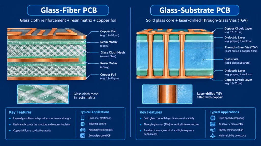
Glass PCB Structural Difference: Glass-Fiber Reinforced vs Solid Glass-Substrate Core
Glass‑fiber PCB uses glass fibers inside a polymer resin matrix; glass‑substrate PCB uses a continuous glass material as the structural substrate. Their materials, interconnect technologies, processing methods and supplier requirements are different.
| Parameter | Glass‑Fiber PCB | Glass‑Substrate PCB |
|---|---|---|
| Glass function | Reinforcement | Structural substrate |
| Resin | Major dielectric component | Usually build‑up dielectric around/over core |
| Manufacturing maturity | Mature PCB technology | Emerging advanced‑substrate technology |
| Conventional PTH | Yes | Not necessarily |
| HDI microvias | Common | Build‑up interconnects possible |
| TGV | Not applicable to conventional glass cloth | Core technology |
| Dimensional stability | Depends on laminate construction | Major architectural advantage |
| Primary concern | Resin/glass distribution and CTE behavior | Glass processing, TGV, alignment and stress |
| Typical equipment | LDI, drilling, lamination, plating, AOI | Precision laser, glass modification/etching, TGV plating, advanced build‑up |
| Typical market | Industrial, automotive, medical, telecom | AI/HPC, advanced packaging, chiplets, optical systems |
Why does this distinction matter to procurement?
A buyer requesting a “Glass PCB” without defining the architecture may receive completely different manufacturing proposals from different suppliers.
For an RFQ, specify whether you mean: ‑ FR‑4 glass‑fiber PCB ‑ High‑Tg glass‑fiber PCB ‑ Low‑loss glass‑fiber PCB ‑ Glass‑reinforced high‑speed PCB ‑ Glass‑substrate PCB ‑ Glass‑core substrate ‑ TGV glass substrate
That single clarification can eliminate a major source of quotation and engineering confusion.
Which Glass PCB Material Should Engineers Choose?
Select the material from the electrical, thermal, mechanical and manufacturing requirements rather than choosing “glass” as a material category by itself.
A practical material‑selection framework is:
| Requirement | Material Direction | Engineering Reason |
|---|---|---|
| General‑purpose PCB | Standard FR‑4 | Balanced cost and manufacturability |
| Higher operating temperature | High‑Tg FR‑4 | Greater thermal margin |
| High‑speed transmission | Low‑loss glass‑fiber laminate | Lower dielectric loss |
| Tight impedance control | Controlled dielectric construction | Better Z0 consistency |
| High‑density routing | HDI‑compatible laminate | Supports microvia structures |
| High thermal cycling | Low‑CTE/high‑reliability laminate | Reduced dimensional stress |
| RF/microwave | Low‑Dk/Df laminate | Reduced insertion loss |
| Advanced packaging | Glass core | Flatness and dimensional stability |
| TGV architecture | Dedicated glass substrate | Enables vertical glass interconnection |
Do not compare laminate materials using Tg alone
Tg is important, but it is not enough to determine whether a PCB material is appropriate.
Engineers should evaluate: ‑ Tg ‑ Td ‑ CTE ‑ Dk ‑ Df ‑ Z‑axis expansion ‑ Moisture absorption ‑ Copper adhesion ‑ Peel strength ‑ Thermal conductivity ‑ Glass style ‑ Resin content ‑ Frequency‑dependent dielectric behavior ‑ CAF resistance ‑ Thermal cycling performance
For high‑speed applications, Dk and Df must always be tied to the material grade, frequency and test method. A generic “low‑Dk glass PCB” statement is not sufficient for a controlled design.
How Does Glass Fiber Affect PCB Mechanical and Electrical Performance?
Glass fiber increases laminate mechanical stability, but its distribution, weave structure, resin content and orientation can also influence local dielectric behavior and high‑speed signal propagation. For detailed analysis on mechanical stiffness and flexural‑modulus‑driven board deflection, see Glass Fiber Flexural Modulus in PCB Materials: What Matters?
Mechanical effects
Glass reinforcement contributes to: ‑ Flexural strength ‑ Dimensional stability ‑ Laminate stiffness ‑ Thermal expansion control ‑ Resistance to mechanical deformation
However, the PCB is not mechanically uniform at the microscopic level.
The actual laminate contains: glass bundles + resin‑rich regions + copper + interfaces
These regions can have different mechanical and electrical properties.
Electrical effects
At high frequencies, a differential pair traveling directly across a glass weave does not see a perfectly uniform dielectric environment.
This can contribute to: ‑ Local impedance variation ‑ Differential skew ‑ Mode conversion ‑ Insertion‑loss variation ‑ Timing uncertainty
For conventional low‑speed designs, this effect may be negligible.
For high‑speed links, it can become part of the channel‑loss and skew budget.
Engineering response
For demanding high‑speed designs, engineers may consider: ‑ Glass style optimization ‑ Spread‑glass constructions ‑ Trace routing relative to glass weave ‑ Symmetrical stackups ‑ Controlled resin content ‑ Low‑loss dielectric materials ‑ Smooth copper foil ‑ 2D/3D electromagnetic simulation
The important point is that glass fiber is not simply a mechanical filler. At high data rates, the glass/resin architecture becomes part of the electrical design.
What Does Glass Transition Temperature Mean for Glass PCB Reliability?
Glass transition temperature, or Tg, is the approximate temperature region where a thermoset resin changes from a relatively rigid glassy state toward a softer rubbery state. It is an important thermal‑design parameter, but it should not be treated as the maximum operating temperature.
For PCB procurement, Tg should be evaluated together with: ‑ Td ‑ CTE ‑ Z‑axis expansion ‑ Thermal decomposition behavior ‑ Thermal cycling ‑ Soldering exposure ‑ Resin system ‑ Copper adhesion ‑ Number of reflow cycles
Why is Tg important during manufacturing?
During PCB fabrication and assembly, the board may experience: ‑ Lamination temperatures ‑ Multiple press cycles ‑ Lead‑free reflow ‑ Thermal shock ‑ Thermal cycling ‑ Localized heating
If the laminate is not properly selected, excessive dimensional movement or mechanical stress can affect: ‑ Registration ‑ Hole reliability ‑ Via reliability ‑ Pad alignment ‑ Layer‑to‑layer geometry
High‑Tg does not automatically mean higher reliability
A material with a higher Tg can still fail if: ‑ Z‑axis expansion is poorly controlled ‑ Copper adhesion is inadequate ‑ Lamination is inconsistent ‑ Microvias are poorly formed ‑ The stackup is mechanically unbalanced ‑ Thermal cycling exceeds the material’s validated capability
Therefore, the procurement question should be: What material system and process combination meets the actual thermal and reliability requirement? rather than: What is the highest Tg available?. For manufacturing‑oriented guidance on high‑Tg laminate selection, lamination control and high‑temperature PCB production, see High‑Tg PCB Manufacturer for High‑Temperature Applications.
How Does Glass PCB Manufacturing Differ From Conventional PCB Manufacturing?
Glass‑fiber PCB manufacturing follows the established PCB process chain, while glass‑core PCB manufacturing introduces additional challenges in glass processing, precision alignment, TGV formation and stress management.
Conventional glass‑fiber PCB process
Material preparation ↓ Inner‑layer imaging ↓ Etching ↓ Layer alignment ↓ Lamination ↓ Mechanical / laser drilling ↓ Desmear ↓ Electroless copper ↓ Electroplating ↓ Outer‑layer imaging ↓ Pattern plating / etching ↓ Solder mask ↓ Surface finish ↓ Electrical testing ↓ AOI / X‑ray / microsection ↓ Final inspection
Glass‑core process concept
Glass substrate preparation ↓ Precision alignment ↓ Glass via formation ↓ TGV cleaning / treatment ↓ Conductive metallization ↓ TGV filling or plating ↓ Build‑up dielectric ↓ Fine‑line redistribution ↓ Microvia formation ↓ Copper patterning ↓ Inspection and reliability validation
The second process requires tighter control of mechanical stress, alignment and interconnect formation.
Which Advanced Manufacturing Technologies Matter for Glass PCB?
The critical technologies are not defined by machine names alone; they are process‑control systems that reduce alignment error, conductor variation, dielectric inconsistency and hidden reliability defects.
1. Laser Direct Imaging
LDI can improve image registration by directly exposing circuit patterns without relying on conventional phototool alignment.
For high‑density PCB production, important parameters include: ‑ Imaging resolution ‑ Layer‑to‑layer registration ‑ Exposure uniformity ‑ Compensation strategy ‑ Panel distortion mapping
2. mSAP
Modified Semi‑Additive Processing can support finer conductor geometries than conventional subtractive etching.
Its value is particularly relevant when the design requires: ‑ Fine line/space ‑ High‑density routing ‑ Fine‑pitch BGA escape ‑ High I/O density ‑ Reduced conductor width variation
3. UV / CO₂ Laser Drilling
Different laser wavelengths can serve different drilling requirements.
Typical applications include: ‑ Microvias ‑ Blind vias ‑ HDI structures ‑ Small‑diameter openings ‑ Controlled‑depth processing
The engineering objective is not simply achieving a small hole.
The actual requirements include: hole diameter + taper + depth + positional accuracy + copper interface quality + wall condition
4. Vacuum Lamination
Controlled vacuum lamination is critical for reducing: ‑ Voids ‑ Resin starvation ‑ Entrapped air ‑ Uneven dielectric thickness ‑ Local delamination
This becomes increasingly important as stackups become thinner and feature density increases.
5. AOI and X‑Ray
Surface inspection alone cannot detect every internal defect.
Depending on the design, inspection may require: ‑ 2D AOI ‑ 3D AOI ‑ X‑ray ‑ Cross‑section analysis ‑ Electrical testing ‑ TDR ‑ VNA ‑ Microsection analysis
The inspection strategy should be defined by failure risk rather than simply by equipment availability.
How Do LDI, mSAP and Laser Drilling Improve Glass PCB Precision?
These technologies reduce different sources of dimensional variation: LDI controls imaging geometry, mSAP controls fine copper formation, and laser drilling controls small interconnect structures.
| Manufacturing Risk | Primary Control | Verification |
|---|---|---|
| Pattern misregistration | LDI + registration compensation | Optical measurement |
| Fine‑line over‑etch | mSAP / controlled plating | Microsection |
| Microvia positional error | Laser drilling | AOI / X‑ray / cross‑section |
| Via wall damage | Laser parameter optimization | Cross‑section |
| Resin voids | Vacuum lamination | X‑ray / microsection |
| Impedance variation | Dielectric thickness + copper geometry control | TDR |
| Hidden interconnect defect | X‑ray / microsection | Reliability testing |
A good supplier should therefore be able to explain which process controls which defect, rather than simply providing a list of equipment brands.
How Does Glass PCB Manufacturing Affect High‑Speed Signal Integrity?
Signal integrity depends on the combined effect of dielectric properties, copper roughness, trace geometry, glass weave, layer registration, via structure and impedance control.
For high‑speed PCB design, engineers should evaluate:
Dielectric loss
Loss increases with: ‑ Higher dielectric loss tangent ‑ Longer routing distance ‑ Higher frequency ‑ Poor material selection
Copper roughness
At high frequencies, current distribution becomes increasingly concentrated near conductor surfaces.
Copper roughness can therefore increase conductor loss.
For high‑speed designs, suppliers may need to specify: ‑ Standard copper ‑ RTF copper ‑ VLP copper ‑ HVLP copper
The exact copper specification should be matched to the signal‑speed requirement and laminate system.
Impedance
A controlled‑impedance PCB should define: ‑ Target impedance ‑ Differential or single‑ended ‑ Trace width ‑ Trace spacing ‑ Copper thickness ‑ Dielectric thickness ‑ Material Dk ‑ Manufacturing tolerance
For example: 100 Ω differential pair
is not a complete manufacturing specification.
A manufacturer also needs enough stackup information to determine how that 100 Ω target is physically achieved.
Via discontinuity
At high data rates, vias can become significant discontinuities.
Important parameters include: ‑ Via stub length ‑ Barrel diameter ‑ Pad diameter ‑ Antipad geometry ‑ Back‑drilling requirement ‑ Microvia structure ‑ Reference‑plane continuity
For advanced high‑speed designs, simulation and measurement should be treated as part of manufacturing validation rather than optional documentation.
What Are the Main Glass PCB Manufacturing Defects?
The most important defects are usually related to registration, resin distribution, thermal expansion, microvia reliability, conductor geometry and hidden internal structures.
1. Layer‑to‑layer registration error
Mechanism: Different materials expand and contract differently during lamination.
Effect: ‑ Pad misalignment ‑ Via breakout ‑ Reduced annular ring ‑ BGA connection risk
Control: ‑ Stackup symmetry ‑ Material characterization ‑ Lamination compensation ‑ Registration measurement
2. Glass‑weave‑induced signal variation
Mechanism: Conductors can cross glass‑rich and resin‑rich regions.
Effect: ‑ Local dielectric variation ‑ Differential skew ‑ Impedance variation
Control: ‑ Glass style selection ‑ Routing strategy ‑ Spread‑glass construction ‑ Electromagnetic simulation
3. Microvia cracking
Mechanism: Repeated thermal expansion creates stress at the microvia/copper interface.
Effect: ‑ Electrical intermittency ‑ Open circuit ‑ Reliability failure after thermal cycling
Control: ‑ Laser parameter optimization ‑ Proper desmear ‑ Copper interface control ‑ Controlled via fill ‑ Microsection validation
4. Resin starvation and voids
Mechanism: Inadequate resin flow or poor lamination conditions can create local defects.
Effect: ‑ Delamination ‑ Reduced mechanical strength ‑ Local impedance variation ‑ Reduced thermal reliability
Control: ‑ Correct prepreg selection ‑ Resin‑flow calculation ‑ Vacuum lamination ‑ Pressure/temperature profiling ‑ Cross‑section inspection
5. Warpage and bow/twist
Mechanism: Uneven copper distribution, asymmetric stackup and thermal mismatch.
Effect: ‑ Assembly problems ‑ BGA soldering defects ‑ Connector misalignment ‑ Mechanical interference
Control: ‑ Symmetrical stackup ‑ Copper balancing ‑ Controlled lamination ‑ Post‑lamination measurement
6. Copper roughness‑related loss
Mechanism: High‑frequency current interacts with the copper surface profile.
Effect: ‑ Increased insertion loss ‑ Reduced channel margin
Control: ‑ Low‑roughness copper ‑ Appropriate surface treatment ‑ Material‑specific channel simulation
How Should Buyers Qualify a Glass PCB Manufacturer?
Qualify the supplier against the exact material, stackup, interconnect, dimensional, electrical and reliability requirements of the project—not against a generic “Glass PCB” capability statement.
Supplier qualification checklist
| Qualification Area | What to Verify |
|---|---|
| Material | Exact laminate manufacturer and grade |
| Tg | Datasheet value and test method |
| Dk/Df | Frequency and test method |
| Layer count | Prototype and production capability |
| Trace/space | Minimum production geometry |
| Registration | Actual production tolerance |
| Laser | Via diameter, depth and positional capability |
| Lamination | Press control and process window |
| Plating | Copper thickness and uniformity |
| Via fill | Required structure and reliability |
| Inspection | AOI, X‑ray, microsection |
| Electrical test | Flying probe / fixture / functional test |
| SI validation | TDR / VNA where required |
| Reliability | Thermal cycling / IST / other qualification |
| Quality system | Relevant certification and traceability |
| NPI | Engineering and DFM support |
| Mass production | Yield and process‑control evidence |
Ask the supplier for evidence
A technically mature supplier should be able to provide some combination of: ‑ Cross‑section images ‑ Capability tables ‑ Material datasheets ‑ Sample stackups ‑ Registration measurements ‑ Microvia sections ‑ Impedance reports ‑ Reliability test reports ‑ First Article Inspection records ‑ Process‑control documentation
The strongest evidence is not:
“We can manufacture it.”
The stronger answer is:
“Here is the process window, measurement method, inspection method and qualification evidence supporting the capability.”
What Should a Glass PCB RFQ Include?
A useful Glass PCB RFQ should define the electrical, mechanical, material, interconnect, finish, testing, quantity and delivery requirements.
Minimum RFQ package
1. Design files
Provide: ‑ Gerber or ODB++ ‑ Drill files ‑ IPC‑2581 where available ‑ Pick‑and‑place files if assembly is required ‑ Fabrication drawing ‑ Stackup
2. Board construction
Specify: ‑ Layer count ‑ Board length/width ‑ Finished thickness ‑ Copper thickness ‑ Inner/outer copper ‑ Material ‑ Tg ‑ Dk/Df ‑ Surface finish
3. HDI requirements
Define: ‑ Microvia diameter ‑ Via‑in‑pad ‑ Stacked microvia ‑ Staggered microvia ‑ Buried vias ‑ Blind vias ‑ Back drilling
4. Signal‑integrity requirements
Specify: ‑ Single‑ended impedance ‑ Differential impedance ‑ Tolerance ‑ Frequency range ‑ Insertion‑loss target ‑ Return‑loss target ‑ TDR requirement ‑ VNA requirement
5. Reliability requirements
Define: ‑ Thermal cycling ‑ Thermal shock ‑ Reflow cycles ‑ IST ‑ CAF ‑ Moisture sensitivity ‑ Mechanical requirements
6. Quantity and delivery
Include: ‑ Prototype quantity ‑ Pilot quantity ‑ Mass‑production quantity ‑ Annual demand ‑ Required delivery date ‑ Packaging requirements
How Much Does Glass PCB Manufacturing Cost?
Glass PCB cost depends on material, geometry, layer count, yield, interconnect technology, testing and production volume; there is no reliable universal price per square inch.
A useful cost model is: Total PCB Cost = Material + Fabrication + Engineering + Tooling + Testing + Yield Loss + Logistics
Major cost drivers
Material cost
Higher‑performance materials generally increase: ‑ Laminate cost ‑ Copper cost ‑ Processing requirements ‑ Inventory requirements
Layer count
More layers increase: ‑ Material consumption ‑ Lamination cycles ‑ Drilling ‑ Plating ‑ Inspection ‑ Yield risk
HDI complexity
Stacked microvias, via‑in‑pad and fine‑line structures increase process steps.
Fine‑line processing
Very small trace/space geometries may require: ‑ LDI ‑ mSAP ‑ Additional plating control ‑ More inspection ‑ Tighter process windows
Testing
High‑speed and high‑reliability boards may require: ‑ TDR ‑ VNA ‑ Microsection ‑ X‑ray ‑ Thermal cycling ‑ IST ‑ Special electrical testing
How can buyers reduce cost?
Do not start by asking for a lower unit price.
Instead, optimize:
- Material architecture
- Layer count
- Via structure
- Copper thickness
- Finished thickness
- Surface finish
- Test requirements
- Panel utilization
- Prototype quantity
- Design‑for‑manufacturing rules
A small change in stackup or via architecture can sometimes reduce several downstream process steps.
What Applications Use Glass PCB Technology?
Glass‑fiber PCBs are already widely used across electronics, while glass‑core structures are being developed for applications requiring extreme dimensional stability, high interconnect density or advanced packaging architectures.
Glass‑fiber PCB applications
‑ Automotive electronics ‑ Industrial controls ‑ Medical electronics ‑ Telecom equipment ‑ Networking ‑ Power electronics ‑ Instrumentation ‑ Consumer electronics ‑ Aerospace electronics
High‑performance glass‑fiber PCB applications
‑ High‑speed networking RF equipment Datacenter electronics 5G/6G systems Automotive radar, which can leverage high‑frequency embedded‑component PCB architectures for miniaturized RF modules, High‑density computing Advanced industrial controls
Glass‑core / glass‑substrate applications
The emerging glass‑core segment is particularly relevant to: ‑ AI accelerators ‑ HPC packages ‑ Chiplet architectures ‑ Advanced semiconductor packaging ‑ Optical/electrical co‑packaging ‑ High‑density interconnect structures
These applications should not be confused with conventional FR‑4 manufacturing.
What Is the Future of Glass PCB Manufacturing ?
The most important development is the convergence of conventional high‑performance glass‑fiber PCB technology with emerging glass‑core substrate technology for AI, HPC, high‑speed interconnect and advanced packaging.
Three technology directions deserve particular attention.
1. Higher‑performance glass‑fiber laminates
As data rates increase, PCB designers are demanding: ‑ Lower Df ‑ Better Dk consistency ‑ Lower copper roughness ‑ Better dimensional stability ‑ Better thermal reliability
The glass‑resin structure becomes increasingly important to channel performance.
2. Glass‑core substrates
Glass‑core technology is moving beyond laboratory discussion toward serious advanced‑packaging development.
The architecture uses glass as a structural core and can use Through‑Glass Vias (TGVs) to provide vertical electrical connections.
The major engineering challenges include: ‑ TGV formation ‑ TGV metallization ‑ Copper/glass CTE mismatch ‑ Glass cracking ‑ Via stress ‑ Alignment ‑ Build‑up dielectric compatibility ‑ Fine‑line redistribution
3. AI and high‑density computing
AI systems continue to increase requirements for: ‑ Interconnect density ‑ Power delivery ‑ Signal integrity ‑ Thermal management ‑ Package size ‑ Dimensional stability
Glass is attractive in advanced packaging because its physical stability can help address some of the scaling challenges associated with larger and denser packages.
However, glass‑core technology remains a specialized advanced‑substrate field. A conventional PCB supplier should not automatically claim TGV mass‑production capability simply because it can manufacture glass‑fiber FR‑4 boards.
Why Choose Shenzhen Hongda Circuit Technology for Glass PCB Manufacturing?
Shenzhen Hongda Circuit Technology approaches Glass PCB projects as an engineering and manufacturing problem rather than treating “glass PCB” as a single material category.
Our engineering evaluation focuses on: Material → Stackup → Geometry → Interconnect → Manufacturing Process → Inspection → Reliability
Engineering support
For demanding PCB projects, the engineering process can include: ‑ DFM review ‑ Stackup review ‑ Material selection ‑ Impedance planning ‑ HDI feasibility analysis ‑ Microvia analysis ‑ Manufacturing tolerance review ‑ Thermal considerations ‑ Reliability planning ‑ Prototype validation ‑ Production transfer
Advanced PCB manufacturing technologies
Depending on the approved design and material system, the manufacturing process can incorporate technologies such as: ‑ LDI ‑ Laser drilling ‑ HDI ‑ mSAP ‑ Controlled lamination ‑ Precision plating ‑ AOI ‑ X‑ray inspection ‑ Microsection analysis ‑ Electrical testing ‑ TDR‑based impedance verification
Important capability qualification statement
Not every Glass PCB requirement should be assumed to be covered by a standard production flow.
For unusual glass‑substrate, TGV, ultra‑fine‑line or advanced‑package structures, capability should be confirmed during engineering review before quotation or production commitment.
This is especially important for: ‑ Glass‑core substrates ‑ TGV structures ‑ Advanced semiconductor packaging ‑ Ultra‑fine redistribution layers ‑ Special glass materials ‑ Non‑standard dielectric systems
The goal is to match the manufacturing process to the engineering requirement—not to force every design into a conventional PCB process.
Glass PCB Procurement FAQ
How do I choose a reliable Glass PCB manufacturer?
Choose a supplier that can demonstrate capability with the exact material, layer structure, line/space, via technology, impedance requirements and reliability testing required by your project.
Ask for capability evidence, sample cross‑sections, material documentation, inspection methods and NPI/DFM support rather than relying only on a generic capability list.
What is the difference between glass‑fiber PCB and glass‑substrate PCB?
Glass‑fiber PCB uses glass fibers embedded in resin, while glass‑substrate PCB uses a continuous glass substrate as the structural core.
Glass‑fiber PCB is an established PCB technology. Glass‑core PCB is an emerging advanced‑substrate architecture commonly associated with TGV and high‑density packaging.
What information should I provide when requesting a Glass PCB quotation?
Provide the Gerber/ODB++ files, stackup, board dimensions, layer count, copper thickness, laminate grade, Tg, Dk/Df requirements, via structure, impedance requirements, surface finish, quantity, testing requirements and delivery target.
For advanced glass structures, also specify whether the project requires a glass core, TGV, redistribution layers or other specialized interconnect technology.
Can a conventional FR‑4 PCB manufacturer produce glass‑core PCB substrates?
Not necessarily.
A supplier capable of manufacturing glass‑fiber FR‑4 boards may not have the specialized equipment, process control or reliability qualification required for glass‑core/TGV substrates.
The buyer should separately verify: ‑ Glass processing ‑ TGV formation ‑ TGV metallization ‑ Glass handling ‑ Precision alignment ‑ Build‑up processing ‑ Copper/glass stress management ‑ Reliability validation
How can I reduce Glass PCB manufacturing cost without reducing reliability?
Optimize the architecture before optimizing the supplier’s unit price.
The highest‑impact opportunities usually include: ‑ Reducing unnecessary layers ‑ Simplifying via structures ‑ Optimizing panel utilization ‑ Selecting the correct laminate ‑ Avoiding unnecessary ultra‑fine geometry ‑ Matching testing to actual risk ‑ Designing for manufacturing ‑ Increasing production volume where appropriate
The objective should be lower total manufacturing cost at the required reliability level, not simply the lowest initial quotation.
Glass PCB Engineering Decision Matrix
Before selecting a Glass PCB supplier, engineers and procurement teams can use the following decision sequence:
| Question | Engineering Decision |
|---|---|
| Is the glass only reinforcement? | Consider glass‑fiber PCB |
| Is high temperature required? | Evaluate high‑Tg materials |
| Is high‑speed transmission required? | Evaluate Dk/Df, copper roughness and glass weave |
| Is very high density required? | Evaluate HDI/mSAP |
| Is extreme dimensional stability required? | Consider glass‑substrate architecture |
| Are TGVs required? | Qualify a specialized glass‑core process |
| Are high‑frequency signals involved? | Require material/frequency‑specific SI data |
| Is thermal cycling severe? | Evaluate CTE and reliability data |
| Is the PCB production volume high? | Optimize panelization and yield |
| Is the design difficult to manufacture? | Perform DFM before quotation |
Glass PCB RFQ Checklist
Before sending your RFQ, confirm that you have defined: ‑ [ ] Glass‑fiber or glass‑substrate architecture ‑ [ ] Exact material grade ‑ [ ] Layer count ‑ [ ] Finished thickness ‑ [ ] Copper thickness ‑ [ ] Minimum trace/space ‑ [ ] Minimum via diameter ‑ [ ] Microvia structure ‑ [ ] Via fill requirement ‑ [ ] Impedance targets ‑ [ ] Dk/Df requirements ‑ [ ] Surface finish ‑ [ ] Board dimensions ‑ [ ] Thermal requirements ‑ [ ] Reliability requirements ‑ [ ] Inspection requirements ‑ [ ] Prototype quantity ‑ [ ] Production quantity ‑ [ ] Delivery requirement
Final Engineering Perspective
Glass PCB is not simply a different PCB material.
It is a manufacturing and procurement decision involving: substrate architecture + material behavior + dimensional stability + interconnect technology + signal integrity + thermal reliability + supplier process capability.
For conventional electronics, glass‑fiber‑reinforced PCB technology remains the practical foundation.
For increasingly demanding high‑speed, high‑density and advanced‑packaging applications, engineers are also evaluating glass substrates and glass‑core architectures.
The correct approach is therefore not:
“Which Glass PCB is the best?”
It is:
“Which glass‑based PCB architecture, material system and manufacturing process can meet the required electrical, mechanical, thermal and reliability targets at production scale?”
That is the question a qualified engineering and manufacturing partner should help answer before the RFQ becomes a production problem.
About Author
David Chen https://www.linkedin.com/in/pcbcoming
David Chen boasts an extensive professional background in PCBA manufacturing, PCBA testing, and PCBA optimization, with specialized expertise in high-precision PCBA fault analysis and rigorous PCBA reliability testing. The author has worked with high-layer-count server PCB fabrication, ultra-low-loss backplane stackups, and thermo-mechanical reliability optimization for AI infrastructure projects involving 112G and 224G PAM4 architectures. Skilled in complex circuit design and cutting-edge advanced PCB manufacturing processes, he delivers solutions that elevate product durability and performance across industrial applications. His technical articles focusing on PCBA manufacturing workflows and testing methodologies are widely cited by industry peers, research institutions, and technical platforms, solidifying his reputation as a recognized technical authority in the global circuit board manufacturing sector.