Ultra-Thin Core PCB: A Procurement Engineer’s Guide to Material Selection, Manufacturing Tolerance, and Supplier Qualification
Ultra-Thin Core PCB technology is where the conversation shifts when your product roadmap demands a finished board below 0.6 mm—this is no longer a question of general PCB capability, but of ultra-thin core discipline. The core—the insulating substrate sandwiched between copper layers—consumes the majority of your thickness budget. Get the core wrong, and no amount of routing refinement will save the assembly from enclosure interference, connector mismatch, or field reliability failure. Before defining your substrate specification, review practical manufacturing limits in our complete ultra‑thin PCB thickness guide.
This guide is written for procurement engineers, hardware program managers, and supply-chain professionals who need to qualify an ultra-thin PCB core supplier without becoming process chemists. We cover the material science, the thickness tolerance realities, the stackup architecture, and the factory-floor capabilities that separate a vendor who simply claims thin-core expertise from one who consistently ships thin core multilayer PCB panels within spec.
What Is an Ultra-Thin PCB Core and Why It Dictates Your Finished Board Thickness
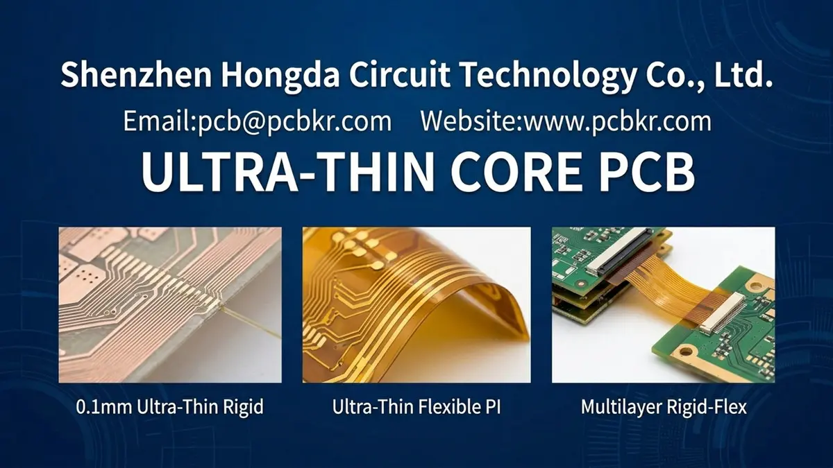
An ultra thin core PCB is not merely a standard board machined down after fabrication. It is built from the ground up using a thin or ultra-thin core material—typically FR-4, BT resin, or polyimide—whose thickness is intentionally selected to constrain the final laminate height. The core provides the dielectric spacing, mechanical rigidity, and thermal stability upon which every subsequent layer depends.
The Difference Between Core Thickness and Finished PCB Thickness
Procurement teams routinely conflate these two figures, and the misunderstanding causes costly redesigns. The PCB core thickness refers only to the substrate layer itself. The finished PCB thickness adds copper foil, prepreg bonding sheets, plated copper, solder mask, and surface finish. A 0.1 mm core can become a 0.18 mm finished board after two copper layers and ENIG treatment—or a 0.35 mm board if you stack four cores with heavy copper and thick prepreg.
At Shenzhen Hongda Circuit Technology Co., Ltd. , our DFM team begins every ultra thin laminate PCB inquiry by asking for the finished thickness target first, then reverse-calculating the core and prepreg combinations that can hit it. This prevents the classic buyer mistake: specifying a 0.2 mm core when the enclosure only has 0.25 mm of total clearance.
How Thin PCB Core Dimensions Cascade Through Your Stackup Design
Each core layer in a multilayer build contributes its full nominal thickness plus resin flow during lamination. When you move from a standard 0.4 mm core to a thin PCB core at 0.1 mm, you gain routing density but sacrifice mechanical forgiveness. Thin cores bow more easily during conveyance, delaminate if desmear is too aggressive, and require symmetric copper distribution to prevent warpage. These constraints must be locked into the stackup before a single trace is routed.
Ultra Thin Core PCB Material Options: FR4, BT Resin, and Flexible Core Materials Compared
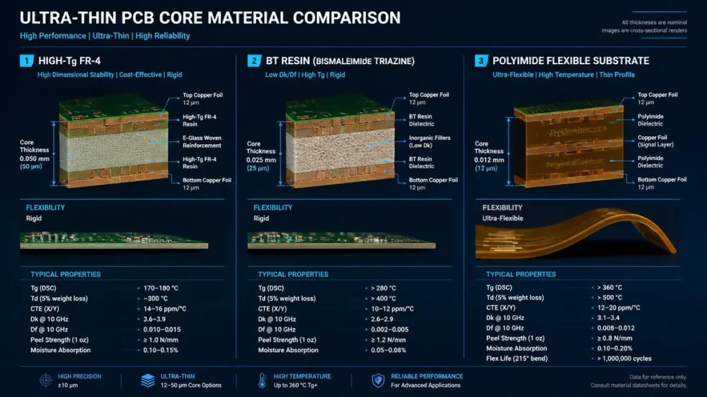
Ultra-Thin PCB Core Material Comparison: High-Tg FR-4 vs BT Resin vs Polyimide
Material selection for an ultra-thin PCB core is not a one-size-fits-all decision. The core material determines the glass-transition temperature (Tg), coefficient of thermal expansion (CTE), dielectric constant (Dk), and flexural modulus. Choose the wrong substrate for your thermal or signal environment, and the board will fail long before the components do.
FR4 Core Material for Rigid Ultra-Thin Laminate PCB Structures
High-Tg FR-4 remains the workhorse for rigid ultra thin laminate PCB applications. In 2026, filled high-Tg variants (Tg 170–180 °C) offer improved dimensional stability and lower z-axis CTE—critical when the core is thin enough that CTE mismatch between copper and resin becomes a dominant stress driver. FR-4 cores down to 0.075 mm are commercially available and compatible with standard lamination cycles, making them the default choice for consumer electronics, industrial controllers, and automotive sensor modules where cost and supply continuity matter.
At Hongda Circuit, we stock Shengyi and Nan Ya high-Tg FR-4 thin cores in 0.1 mm, 0.127 mm, and 0.152 mm gauges, with lot-traceable CTE data. This allows our engineers to run warpage simulation before tooling, not after the first article fails flatness inspection.
BT Core Material When Signal Integrity Demands Exceed Standard FR4
BT (bismaleimide-triazine) resin systems occupy the middle ground between FR-4 and PTFE. With Tg values of 180–200 °C, moisture absorption below 0.3 %, and Dk/Df performance superior to standard epoxy, BT core material is the logical choice for ultra thin laminate PCB builds that must survive multiple lead-free reflow cycles while preserving high-frequency signal integrity. BT is particularly prevalent in smartphone motherboard substrates, 5G small-cell modules, and automotive ADAS camera boards where the core is thin but the electrical specification is aggressive.
The trade-off is processing sensitivity. BT resins cure at higher temperatures and are more prone to warpage if lamination pressure or cooling rates are not tightly controlled. Not every factory that laminates FR-4 can handle BT thin cores without yield loss.
Flexible Core Material for Bendable Ultra-Thin PCB Applications
When the end product must flex, fold, or conform to an irregular surface, polyimide (PI) becomes the thin PCB core material of choice. Modified PI and colorless PI (CPI) substrates achieve Tg values above 250 °C, withstand dynamic bending exceeding 2 million cycles, and can be processed into finished thicknesses below 0.08 mm. These materials are not “soft FR-4″—they require dedicated flex-circuit fabrication lines with tension-controlled conveyance and adhesiveless copper cladding to prevent crease fractures.
Hongda Circuit operates separate rigid and flexible production lanes. Our flex-line handles PI-based ultra thin core PCB builds down to 0.05 mm finished thickness, with coverlay lamination and selective stiffener attachment for hybrid rigid-flex assemblies.
Material Selection Matrix for Thin Core Multilayer PCB Builds
| Core Material | Typical Thickness Range | Tg (°C) | Best For | Caution |
|---|---|---|---|---|
| High-Tg FR-4 | 0.075–0.3 mm | 170–180 | Cost-driven rigid consumer/industrial | Higher CTE than BT; watch warpage below 0.1 mm |
| BT Resin | 0.1–0.2 mm | 180–200 | High-frequency, high-reliability rigid | Requires controlled lamination; longer cure cycles |
| Polyimide (PI) | 0.025–0.1 mm | 250+ | Flexible and rigid-flex wearables | Adhesiveless processing only; no standard FR-4 lamination |
Ultra Thin Core PCB Thickness Range: From 0.075 mm to 0.6 mm Design Windows
The term “ultra-thin” is relative. In PCB procurement, it helps to anchor the conversation to actual numbers rather than marketing labels. The following thicknesses represent the practical design windows our engineering team encounters daily when quoting ultra thin core PCB projects.
Standard Thin PCB Core Thickness Options Available in 2026
- 0.075 mm (3 mil): The lower practical limit for mass-produced FR-4 cores. Used in single- and double-sided builds where every micron counts, such as smart-card inlays and ultra-slim sensor carriers.
- 0.1 mm (4 mil): A common sweet spot for 4-layer consumer electronics. Provides enough mechanical integrity for SMT assembly while keeping finished boards under 0.4 mm.
- 0.127 mm (5 mil): Frequently specified for 6-layer smartphone sub-boards. Offers a balance between routing density and handling robustness during panel plating.
- 0.152 mm (6 mil): The transition zone where standard multilayer techniques still apply, but thin-core discipline is required to hold overall thickness under 1.0 mm.
- 0.18–0.22 mm: Technically “thin” rather than “ultra-thin,” yet still demands core-aware stackup planning when paired with heavy copper or thick prepreg.
- 0.3–0.6 mm: Standard thin-core territory for industrial and automotive modules where the enclosure allows modest height but weight reduction is prioritized.
Why Core Thickness Tolerance Becomes Critical Below 0.2 mm
Standard IPC-6012 tolerance for finished board thickness is ±10 %. On a 1.6 mm board, that is ±0.16 mm—usually harmless. On a 0.2 mm finished ultra thin laminate PCB, ±10 % becomes ±0.02 mm, which can swallow your entire solder-paste stencil gap or violate connector insertion depth. At Hongda Circuit, we hold thin PCB core thickness to ±0.025 mm (±1 mil) on cores below 0.2 mm, and we communicate this constraint to buyers during the quotation phase so enclosure designers can allocate tolerance budgets realistically.
Thin Core Multilayer PCB Stackup Architecture: Layer Count vs. Total Thickness
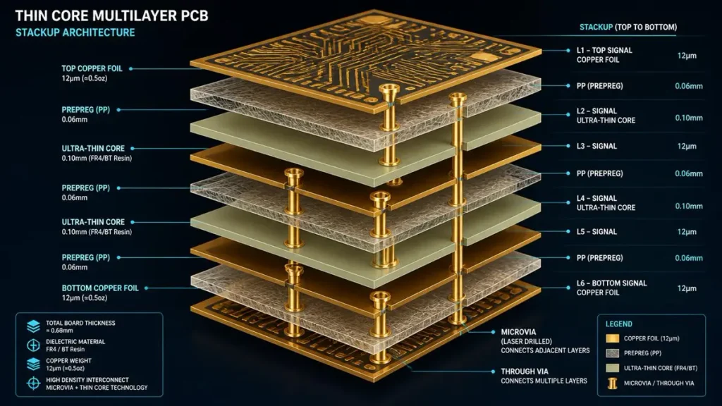
Thin Core Multilayer PCB Stackup Architecture with 0.1mm Core and Laser Microvias
The real engineering challenge of thin core multilayer PCB design is not making one layer thin—it is making many layers thin together without creating a board that warps, cracks, or fails impedance targets.
How Thin Core Reduces Overall Board Height Without Sacrificing Layer Count
A 6-layer board built with standard 0.4 mm cores and 0.2 mm prepreg might finish at 1.8 mm. Replace the cores with 0.1 mm thin PCB core material and thin the prepreg to 0.076 mm, and the same 6-layer stackup can finish below 0.8 mm. The signal integrity implications are significant: thinner dielectrics reduce trace widths for a given impedance, which increases routing density, which allows smaller board area, which reduces system cost. This is why smartphone motherboard designers aggressively pursue thin core multilayer PCB architectures.
The penalty is thermal and mechanical. Thinner dielectrics conduct heat less effectively across the plane, and thinner cores offer less resistance to bending moment. Your supplier must compensate with higher-Tg materials, symmetric copper distribution, and sometimes embedded copper-coin thermal vias.
Symmetrical Stackup Rules for Thin Core Multilayer PCB Warpage Prevention
Warpage is the silent killer of ultra thin core PCB assemblies. A board that leaves the factory flat can bow 0.8 % during lead-free reflow, preventing BGA solder joint formation and causing head-in-pillow defects. The root cause is almost always asymmetric thermal stress: one side of the board has more copper, thicker cores, or different prepreg resin content than the other.
Our DFM protocol at Hongda Circuit enforces three rules for every thin core multilayer PCB:
- Mirror symmetry: Layer 1 must mirror Layer N in copper weight and coverage percentage. Layer 2 must mirror Layer N-1. Deviations require engineering sign-off.
- Balanced prepreg: Use identical prepreg styles (e.g., two sheets of 2116) on either side of the central plane. Asymmetric glass weave—such as one 7628 sheet on top and one 2313 plus 2116 on bottom—is a known warpage trigger.
- Copper thieving: Where signal layers create large copper-free zones, we add dummy copper fills (thieving) to balance the areal density within 15 % of the opposing layer. This is non-functional copper, but it is functionally essential for flatness.
Ultra Thin Core PCB Manufacturing: Lamination, Alignment, and Process Control
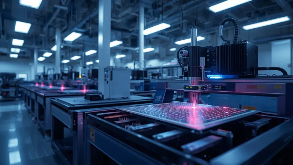
Laser Direct Imaging (LDI) and Precision Processing for Ultra-Thin Core PCBs
Procurement engineers often assume that if a factory can build standard multilayer boards, it can simply “turn down the thickness dial” for ultra thin laminate PCB orders. This assumption is expensive. Thin-core manufacturing requires distinct equipment, process recipes, and handling protocols.
Vacuum Lamination Systems for Ultra-Thin Laminate PCB Bonding
Standard hydraulic presses apply 300–500 psi across the panel. On a thin PCB core below 0.15 mm, that pressure can crush glass fibers, extrude resin beyond the panel edge, or embed copper foil wrinkles into the dielectric. Hongda Circuit uses LAUFFER vacuum lamination systems that apply controlled, uniform pressure in a vacuum environment. The vacuum eliminates air gaps between layers, while the programmable pressure ramp prevents resin starvation or excessive flow. For BT resin ultra-thin PCB core builds, we extend the cure cycle and reduce the cooling rate to 2–3 °C per minute, minimizing differential shrinkage stress.
Laser Direct Imaging (LDI) for ±10 µm Layer-to-Layer Registration
Thin cores are less forgiving of misalignment. A 0.1 mm core with a 0.05 mm microvia has only 0.025 mm of annular ring on each side. If layer-to-layer registration drifts 0.02 mm, the via breaks out. Hongda Circuit employs SCREEN Ledia LDI exposure systems that image directly onto photoresist without film degradation. The ±1.5 µm imaging accuracy, combined with automated optical alignment during lamination, holds interlayer registration within ±10 µm—well inside the safety margin for thin-core microvias.
Copper Weight and Protective Layer Impact on Final Thickness
Buyers frequently specify 1 oz (35 µm) copper out of habit, then wonder why their 0.3 mm finished board measures 0.38 mm. On ultra thin core PCB builds, copper weight is not a free choice; it is a thickness budget line item. A 4-layer board with 1 oz outer and 0.5 oz inner copper adds approximately 0.12 mm of copper alone. Add two 0.1 mm cores, two prepreg layers, solder mask, and ENIG, and you are already at 0.45 mm.
Our standard recommendation for thin core multilayer PCB designs below 0.6 mm finished thickness is:
- Outer layers: 0.5 oz (18 µm) base copper, plated to 1.0 oz finished
- Inner layers: 0.33 oz (12 µm) or 0.5 oz base copper
- Surface finish: ENIG (3–5 µm total added thickness) or OSP (<1 µm) rather than HASL (25–75 µm variable)
How to Evaluate an Ultra Thin Core PCB Manufacturer: A Procurement Checklist
Sourcing ultra thin core PCB fabrication is not a commodity purchase. The wrong supplier will deliver boards that pass electrical test but fail in your assembly line—or worse, in the field.se this checklist during supplier qualification. For full context of end‑to‑end ultra‑thin PCB production and supplier evaluation, refer to our ultra‑thin PCB manufacturing main overview.
Verify In-House mSAP and LDI Capability for Fine-Line Thin Core Builds
If your design includes line/space below 50 µm, subtractive etching is no longer viable. The isotropic undercut becomes uncontrollable, and a 5 µm trace-width variation can shift impedance 2–3 Ω. You need a supplier with mSAP (Modified Semi-Additive Process) in-house: 1.5–3 µm seed layer, LDI imaging, selective plating to height, then flash-etch. Hongda Circuit’s mSAP line has qualified 8 µm/8 µm for substrate-like PCB (SLP) builds, with standard production at 20 µm/20 µm for smartphone and AI edge modules. If a supplier claims fine-line capability but cannot describe their mSAP chemistry and plating line configuration, they are likely subcontracting to a third party—with all the traceability and IP risks that entails.
Assess Material Stock and Certification Depth (ISO 9001, IPC-6012 Class 3)
Ultra thin laminate PCB lead times are driven by material availability, not factory capacity. A 2026 industry survey showed 16–20 week lead times for ultra-low-loss laminates as AI server demand absorbs global supply. Ask your supplier:
- Do they stock thin-core materials, or do they order per project?
- Can they provide material certifications with lot traceability?
- What is their policy on substitution if the specified core is allocated?
Hongda Circuit maintains a 2026-spec material warehouse with Panasonic Megtron 7/8, Isola Astra MT77, Rogers RO4350B, and Taconic RT5880 in thin-core gauges. Our quality system is certified to ISO 9001:2026, AS9100D (Aerospace), IATF 16949 (Automotive), and IPC-6012 Class 3/3A. For medical OEMs, we maintain ISO 13485 compliance on dedicated production lanes.
Demand Pre-Production DFM Review for Thin Core Multilayer PCB Designs
The most expensive mistake in thin core multilayer PCB procurement is submitting a design that was validated electrically but never checked for manufacturability. A proper DFM review for thin-core builds should flag:
- Asymmetric copper distribution and warpage risk
- Core thickness vs. finished thickness mismatch
- Aspect ratio violations on microvias
- Impedance stackup feasibility with available prepreg gauges
- Surface finish thickness contribution to overall height
Hongda Circuit provides this review within 1 hour of Gerber submission, with engineering feedback—not a generic checklist. We have found that 40 % of first-time ultra thin core PCB inquiries contain a stackup error that would have caused a respin if caught later.
Shenzhen Hongda Circuit Technology: 2026 Ultra Thin Core PCB Production Capabilities
Founded in 1999 and headquartered in Shenzhen’s Baoan district, Hongda Circuit has evolved from a standard PCB fabricator into a technology partner for OEMs building next-generation hardware. Our ultra thin core PCB capabilities are not an afterthought; they are a core competency supported by dedicated equipment, trained process engineers, and a material ecosystem designed for thin-core reliability.
Advanced Equipment Portfolio for Ultra-Thin Laminate PCB Fabrication
- SCREEN Ledia LDI Exposure Machine: Direct imaging for soldermask and etch resist, eliminating phototool degradation that causes pad-size variation and plating non-uniformity.
- Mitsubishi UV/CO₂ Laser Drilling: Microvia formation down to 0.075 mm (3 mil), with composite drilling for clean hole walls on thin cores without glass fiber burrs.
- LAUFFER Vacuum Lamination System: Controlled-pressure, vacuum-assisted lamination specifically configured for thin-core and BT resin processing.
- HX Automated Plating Line: Three-in-one horizontal equipment achieving high-density direct copper fill with plating uniformity error within 5 %, ensuring void-free vias.
- Nordson DAGE X-Ray Tester: 3D X-ray inspection for void detection in plated through-holes and microvias before surface finish application.
- XRF Spectrometers (Fischer): Non-destructive gold and nickel thickness measurement with NIST-traceable weekly calibration.
Material Ecosystem and Thickness Control Protocols
We do not force-fit available materials into your design. Our engineering team works backward from your finished thickness, impedance, and thermal targets to specify the core, prepreg, and copper combination that hits the spec with margin. For ultra thin laminate PCB projects, we provide:
- Lot-traceable CTE and Tg data for every core material
- Pre-lamination warpage simulation using stackup symmetry analysis
- Post-lamination flatness verification via laser scanning (target <0.5 % warpage)
- Cross-sectional microsection analysis on first articles to confirm core thickness, prepreg resin flow, and copper plating uniformity
Quality Assurance Framework for Thin Core Multilayer PCB Delivery
- Incoming Material Inspection: All thin-core laminates are checked for thickness deviation, moisture content, and copper peel strength before entering production.
- In-Process AOI: Automated optical inspection after inner-layer etch, outer-layer patterning, and solder mask application.
- Electrical Test: 100 % flying probe or fixture-based continuity/isolation testing.
- Final Inspection: IPC-A-600 Class 3 visual criteria, plus custom flatness measurement for thin boards.
- AI-Driven ERP Tracking: Real-time production monitoring with automated alerts when process parameters drift outside control limits. Our on-time delivery rate exceeds 95 %.
Ultra-Thin Core PCB Specifications at a Glance
| Specification | Hongda Circuit Standard | Notes |
|---|---|---|
| Product Type | Ultra-thin core PCB, thin core multilayer PCB | Rigid, flexible, and rigid-flex configurations |
| Core Materials | FR-4 (Tg 130/170/180), BT resin, Polyimide (PI) | High-Tg filled FR-4 recommended for <0.15 mm cores |
| Core Thickness Range | 0.075 mm – 0.3 mm (standard); 0.025 mm (PI flex) | FR-4 practical minimum: 0.075 mm |
| Finished Board Thickness | 0.1 mm – 0.6 mm (typical ultra-thin range) | Includes copper, prepreg, mask, and finish |
| Layer Count | 2–12 layers (standard thin-core); up to 28 layers (hybrid thin/thick) | Symmetrical stackup mandatory for >4 layers |
| Min. Trace/Space | 20 µm / 20 µm (standard mSAP); 8 µm / 8 µm (SLP qualification) | Subtractive etching available down to 50 µm |
| Microvia Diameter | Blind via 0.05 mm; Buried via 0.08 mm | Laser-drilled; aspect ratio ≤ 0.8:1 for reliability |
| Copper Weight | 0.33 oz (12 µm) – 1 oz (35 µm) base; plated to target | Heavy copper (>2 oz) not recommended for <0.3 mm finished |
| Surface Finish | ENIG, OSP, ENEPIG, Immersion Silver | ENIG preferred for flatness; OSP for minimal thickness add |
| Warpage Control | <0.5 % (standard); <0.3 % (high-reliability option) | Achieved via symmetric stackup + vacuum lamination |
| Quality Standards | ISO 9001, IPC-6012 Class 3/3A, AS9100D, IATF 16949, ISO 13485 | Medical-grade lanes available |
| DFM Response | 1-hour engineering evaluation | Includes stackup feasibility and warpage risk analysis |
| Prototype Lead Time | 24–72 hours (single/double-sided); 5–7 days (multilayer) | Material-dependent; stock cores ship faster |
Frequently Asked Questions by Procurement Teams Sourcing Ultra Thin Core PCBs
How do I know if my supplier actually manufactures ultra thin core PCBs in-house or brokers them to a third party?
Ask for a virtual or on-site tour of their lamination and imaging areas. A legitimate ultra thin core PCB manufacturer will have vacuum lamination presses (not just standard hydraulic), LDI or at least high-resolution DI exposure, and laser drilling capability. Request cross-sectional photos of previous thin-core builds with visible core thickness measurement. At Hongda Circuit, we welcome buyer audits and provide video walkthroughs of our thin-core production lane upon request.
What is the difference between ultra thin core PCB and ultra thin laminate PCB, and which term should I use when requesting a quote?
“Core” refers specifically to the substrate layer. “Laminate” refers to the finished bonded structure (core + copper + prepreg). When you request an ultra thin core PCB, you are signaling that you understand the core thickness drives the design. When you request an ultra thin laminate PCB, you may receive quotes based on finished thickness assumptions that hide core limitations. We recommend specifying both: “Finished thickness 0.3 mm, built with 0.1 mm FR-4 core, 4-layer stackup.” This eliminates ambiguity.
Why do some ultra thin core PCB suppliers quote significantly lower prices than others for the same stackup?
Price divergence in thin core multilayer PCB sourcing usually traces to three factors: (1) Material grade—some vendors quote with standard Tg FR-4 when your design needs high-Tg to survive reflow; (2) Process shortcuts—skipping vacuum lamination or using lower-grade prepreg to save cost, which causes delamination or warpage; (3) Subcontracting—brokers quoting a thin-core job to a generalist factory without thin-core experience. At Hongda Circuit, we itemize material grades, process steps, and inspection protocols in every quotation so buyers can compare apples to apples.
Can I use a thin core multilayer PCB for a design that requires controlled impedance, or is that only possible on standard-thickness boards?
Controlled impedance is absolutely achievable on thin core multilayer PCB builds, but the design rules change. Thinner dielectrics require narrower traces for the same impedance target, which pushes you toward mSAP or advanced subtractive processes. The dielectric thickness tolerance also becomes a larger percentage of the total, so impedance variation can be ±10 % unless your supplier holds tight laminate thickness control. Hongda Circuit provides impedance modeling and TDR verification as part of our DFM service for thin-core designs, ensuring that your 50 Ω or 100 Ω differential pairs remain within spec despite the aggressive stackup.
What documentation should I prepare before contacting an ultra thin core PCB manufacturer to avoid delays in quoting?
To receive an accurate, same-day quote for an ultra thin laminate PCB, prepare: (1) Gerber files and drill files; (2) A stackup drawing or table showing target finished thickness, core material preference, and layer count; (3) Impedance requirements with reference planes specified; (4) Surface finish and solder mask specifications; (5) Quantity breakdown (prototype, NPI, production); and (6) Any mechanical constraints (envelope dimensions, connector keep-out zones, bending requirements for flex). The more specific you are about the thin PCB core material and thickness, the faster we can confirm manufacturability and provide a firm lead time.
Ready to Source Your Ultra-Thin Core PCB?
Shenzhen Hongda Circuit Technology Co., Ltd. specializes in ultra thin core PCB, thin core multilayer PCB, and ultra thin laminate PCB fabrication for OEMs who cannot afford a respin. Our engineering team provides 1-hour DFM feedback, material selection guidance, and stackup optimization to ensure your thin-core design ships on time, within tolerance, and ready for assembly.
Share your target finished thickness, core material, and layer structure to receive a detailed manufacturability review and competitive quotation.
- Website:www.pcbkr.com
- Email:sales@pcbkr.com
- Engineering Support: 24/7 technical consultation
- DFM Review: 1-hour response guarantee
Shenzhen Hongda Circuit Technology Co., Ltd. — Precision Interconnects Since 1999.
About Author
David Chen https://www.linkedin.com/in/pcbcoming
David Chen boasts an extensive professional background in PCBA manufacturing, PCBA testing, and PCBA optimization, with specialized expertise in high-precision PCBA fault analysis and rigorous PCBA reliability testing. The author has worked with high-layer-count server PCB fabrication, ultra-low-loss backplane stackups, and thermo-mechanical reliability optimization for AI infrastructure projects involving 112G and 224G PAM4 architectures. Skilled in complex circuit design and cutting-edge advanced PCB manufacturing processes, he delivers solutions that elevate product durability and performance across industrial applications. His technical articles focusing on PCBA manufacturing workflows and testing methodologies are widely cited by industry peers, research institutions, and technical platforms, solidifying his reputation as a recognized technical authority in the global circuit board manufacturing sector.