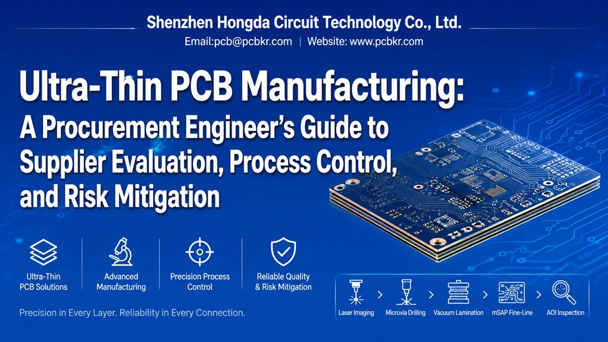
Ultra-Thin PCB Manufacturing: A Procurement Engineer’s Guide to Supplier Evaluation, Process Control, and Risk Mitigation
Introduction: Why Ultra-Thin PCB Manufacturing Keeps Procurement Teams Awake at Night
If you are an OEM procurement manager or hardware engineering lead sourcing ultra-thin PCB manufacturing for next-generation wearables, medical sensors, or AI edge devices, you have probably already learned one hard truth: not every factory that claims “thin board capability” can actually deliver repeatable yields below 0.4 mm total thickness.
The gap between marketing slides and shop-floor reality is where most ultra thin PCB fabrication programs fail. A supplier might list “HDI capability” on their website, yet lack vacuum lamination platens thin enough to prevent resin squeeze-out on 0.1 mm cores. They might promise 50 μm microvias, but their CO₂ laser driller has not been requalified for picosecond pulse widths. These gaps do not surface during the RFQ phase. They surface six months later, when your field units start failing thermal cycling.
This guide is written from the manufacturing floor outward, not from a sales brochure inward. We will walk through the thin PCB manufacturing process step-by-step, flag the failure modes that actually matter for procurement, and give you a verifiable checklist to separate real ultra thin PCB production capability from PowerPoint capability.
1. What Defines Ultra-Thin PCB Manufacturing from a Fabrication Perspective
Before you evaluate suppliers, you need to speak their language. In ultra-thin PCB manufacturing, “thin” is not a subjective description. It is a stack-up constraint that changes every downstream process.
1.1 Thickness Thresholds and Stack-Up Reality
From a thin PCB manufacturing process standpoint, the industry generally draws the line at 0.4 mm finished thickness for standard ultra‑thin boards, with advanced applications pushing into 0.1–0.2 mm territory. Before defining your stack‑up, review practical dimension limits in our complete ultra‑thin PCB thickness procurement guide. At these dimensions, a 4-layer board might use a 100 μm core with 80 μm prepreg dielectrics. That is not simply a thinner version of a standard 1.6 mm stack-up. It is a fundamentally different mechanical structure.
The key difference for procurement: standard HDI process rules do not automatically apply. A fabricator qualified for 1.2 mm, 8-layer HDI might crash yields on a 0.3 mm, 6-layer build because their lamination press cannot hold uniform pressure across such a thin stack without glass-flow variation.
1.2 Material Systems Used in Ultra-Thin PCB Fabrication
Not all thin boards use the same substrate. Your supplier’s material library directly determines reliability:
| Material Category | Typical Thickness | Application | Procurement Note |
|---|---|---|---|
| High-Tg FR-4 | 100–200 μm core | Consumer, industrial | Most common; verify Tg ≥ 170°C for lead-free assembly |
| Polyimide (PI) | 25–75 μm base | Wearables, medical flex | Requires adhesiveless lamination for dimensional stability |
| LCP (Liquid Crystal Polymer) | 25–100 μm | RF, mmWave antennas | Low moisture absorption; higher material cost |
| Modified Epoxy (Low-Dk) | 100–150 μm | High-speed digital | Megtron 6/7 grade; critical for 112G/224G channels |
At Shenzhen Hongda Circuit Technology Co., Ltd., our incoming inspection protocol for ultra thin PCB fabrication includes copper-foil thickness verification to ±1.5 μm and prepreg resin-content testing on every lot. Why? Because on a 0.2 mm board, a 10% resin-flow variation can shift dielectric thickness by 8 μm—enough to break impedance control on a 50 Ω differential pair.
2. Ultra-Thin PCB Manufacturing Process: A Step-by-Step Technical Breakdown
Understanding the thin PCB manufacturing process at a granular level is the only way to audit a supplier’s real capability. Here is how a qualified ultra thin PCB production line actually operates in 2026.
2.1 Substrate Preparation and Ultra-Thin Material Handling
The first hidden risk in ultra-thin PCB manufacturing happens before the first photoresist layer is applied: handling damage.
A 0.1 mm core panel can crease if an operator lifts it from one edge. It can accumulate electrostatic damage during conveyance. It can absorb ambient moisture in under 30 minutes in a humid Shenzhen summer, leading to steam delamination during reflow.
What to verify on your supplier’s factory tour:
- Do they use vacuum-lift conveyors or manual handling for cores below 0.2 mm?
- Is there a pre-bake station (typically 120–150°C for 4–8 hours) before imaging?
- What is their clean-room classification for thin-core storage? (Class 100,000 is acceptable; Class 10,000 is better.)
At PCBKR’s Baoan facility, thin cores move through a dedicated low-tension conveyor line with ionized air knives and edge-support rails. We pre-bake all polyimide and ultra-thin FR-4 cores at 130°C for 6 hours minimum before laser imaging. This is not optional luxury—it is yield protection.
2.2 Inner Layer Pattern Formation for Fine-Line Density
Once the core is clean and stable, the fabricator must define circuit patterns. In ultra thin PCB manufacturing, this is where line-width control becomes critical.
For boards below 0.3 mm, you are almost certainly routing fine-pitch BGAs or 0.35 mm pitch components. That means line/space targets of 25 μm or tighter. Traditional contact-print photolithography using film tooling cannot hold these tolerances on warped thin substrates.
The 2026 standard: Laser Direct Imaging (LDI).
LDI writes the resist pattern directly onto the panel using a UV laser, eliminating film stretch and contact-pressure variables. At PCBKR, our SCREEN Ledia LDI Exposure Machine resolves 8 μm features with layer-to-layer alignment accuracy of ±10 μm. For ultra thin PCB fabrication programs targeting 224G PAM4 or PCIe Gen6, this alignment precision is non-negotiable—misregistration of 20 μm can shift differential impedance by 4–6 Ω.
Etching control is equally critical. Thin copper foils (9 μm or 12 μm) etch faster than standard 18 μm foils. Without differential etch-rate monitoring, you get undercut that turns a 25 μm design width into an 18 μm trace with a trapezoidal cross-section. That geometry variation destroys signal integrity at 56 GHz.
2.3 Vacuum Lamination Technology for Ultra-Thin Multilayer Stacks
Lamination is the heart of ultra thin PCB production—and the most common failure point.
Standard hydraulic presses apply 300–500 psi across a book of panels. On a 1.6 mm stack, pressure distributes relatively evenly. On a 0.3 mm stack with 80 μm prepregs, excessive pressure squeezes resin out of the edges, creating starved regions (dry glass with no resin) in the center of the panel. The result: delamination after two thermal cycles.
The solution is vacuum-assisted lamination.
Vacuum lamination pulls atmospheric pressure down to <50 mbar before the press closes. This removes trapped air between layers and allows the press to use lower mechanical pressure (150–200 psi) while still achieving full resin flow. The outcome: uniform dielectric thickness, minimal squeeze-out, and warpage control below 0.5%—a threshold that even 0.8% warpage can violate for fine-pitch BGA assembly.
At PCBKR, our LAUFFER Lamination System operates with programmable step-pressure profiles: 80 psi penetration stage, 150 psi diffusion stage, and 200 psi cure stage, with vacuum hold throughout. For ultra-thin multilayer PCB fabrication up to 12 layers, we limit book height to 12 mm and use rigid stainless-steel separator plates to prevent Z-axis pressure gradients.
2.4 Laser Microvia Drilling and Interconnect Reliability
Mechanical drilling stops being practical below 200 μm diameter. Bit deflection, runout, and breakage make it unreliable. For ultra thin PCB manufacturing, laser drilling is the only viable path to high-density interconnects.
Two laser technologies dominate in 2026:
- CO₂ lasers (10.6 μm wavelength): Ablate dielectric efficiently but stop at copper due to reflectivity. Ideal for blind vias in build-up layers.
- UV lasers (355 nm): Penetrate both copper and dielectric. Enable 50–75 μm vias and direct copper ablation for ultra-HDI applications.
At PCBKR, our Mitsubishi UV/CO₂ Hybrid Laser Drilling System achieves 75 μm blind microvias with ±5 μm positional accuracy. For rigid-flex ultra thin PCB production, we have additionally qualified picosecond laser sources that cut 50 μm vias in polyimide without thermal damage to adjacent layers.
The post-drill step that separates good suppliers from bad ones: desmear.
Laser ablation leaves resin residue on via walls. If not removed, electroless copper cannot adhere, creating voids that fail thermal cycling. Plasma desmear (using CF₄/O₂ chemistry) is the 2026 gold standard for high-reliability microvia ultra thin PCB fabrication. It removes resin smear without attacking the dielectric surface, unlike aggressive permanganate baths that can over-etch thin cores.
2.5 mSAP and SAP Fine-Line Patterning: Why Subtractive Etching Is No Longer Enough
Here is a procurement insight that will save you from a yield disaster: if your ultra-thin HDI PCB manufacturing program requires line/space below 30 μm, subtractive etching will fail. Period.
Subtractive etching starts with 18 μm copper, images the pattern, and etches away everything else. The problem is undercut—etchant attacks the copper sideways as well as downward. On a 25 μm line, 3 μm of undercut on each side turns your rectangular trace into a 19 μm hourglass. Impedance tolerance explodes.
Modified Semi-Additive Process (mSAP) solves this.
mSAP starts with an ultra-thin copper seed layer (1.5–3 μm), images the trace pattern, and electroplates copper only where needed. A brief flash etch removes the seed between traces. Because almost no copper is removed from the trace itself, sidewalls remain near-vertical.
| Process | Min Line/Space | Trace Geometry | Best For |
|---|---|---|---|
| Subtractive | 50–75 μm | Trapezoidal | Standard multilayer |
| mSAP | 15–30 μm | Near-rectangular | Advanced HDI, substrate-like PCBs |
| SAP | <15 μm | Vertical | IC substrates, chiplet packaging |
At PCBKR, our mSAP line is qualified down to 8 μm line / 8 μm space—a capability we have held in continuous production since Q3 2024 for smartphone motherboard and AI accelerator programs. For procurement teams, this means you can specify substrate-like PCB density without paying IC-substrate factory premiums.
2.6 Outer Layer Processing, Solder Mask, and Surface Finish
Outer layers on ultra thin PCB manufacturing builds follow a similar imaging and etch flow, but with one added constraint: the board is now even more fragile.
Spray-coating solder mask on a 0.2 mm panel can flex the substrate enough to crack inner-layer microvias. Leading ultra thin PCB fabrication houses have moved to curtain-coating or spray systems with vacuum hold-down fixtures that support the panel during application.
For surface finish selection, avoid HASL on boards below 0.3 mm. The thermal shock (260°C molten solder wave) and mechanical stress of air-knife leveling can warp the panel beyond repair. Better options for thin flexible PCB production process and rigid ultra-thin builds:
- ENIG (Electroless Nickel Immersion Gold): Flat, wire-bondable, excellent for fine-pitch BGA. Watch for “black pad” risk on ultra-fine pads; specify ENEPIG if wire-bonding gold is required.
- Immersion Silver: Low profile, good solderability, cost-effective for consumer wearables.
- OSP (Organic Solderability Preservative): Ultra-thin, ideal for cost-sensitive single-sided flex; limited shelf life.
PCBKR’s ENIG line includes XRF spectrometers with NIST-traceable calibration for nickel and gold thickness verification on every production lot. For medical ultra-thin PCB manufacturing programs, we maintain ISO 13485-compliant process lanes with dedicated chemistry baths and lot-traceability documentation.
2.7 Final Inspection and Electrical Testing Protocols
You cannot test a 0.2 mm board the same way you test a 1.6 mm server backplane.
Flying-probe testers apply downward pressure on test points. On a thin substrate, that pressure can flex the board and create false open-circuit readings—or worse, crack microvias. The fix is vacuum hold-down fixtures that support the panel during probing, or transition to dedicated bed-of-nails fixtures for volume production.
AOI (Automated Optical Inspection) systems also need recalibration. The reduced board thickness shifts the focal plane. A supplier running standard AOI recipes on thin boards will generate false defect calls or miss actual opens.
At PCBKR, our inspection protocol for ultra thin PCB production includes:
- 100% 3D AOI with Z-axis calibration for panels <0.4 mm
- 4-wire Kelvin flying probe with vacuum fixture support
- Microsection analysis on first-article and weekly production samples
- Impedance coupon testing to 70 GHz using vector network analyzers for 224G PAM4 builds
3. Critical Manufacturing Challenges in Ultra-Thin PCB Fabrication
Now that you understand the process, here are the three failure modes that actually kill ultra thin PCB fabrication programs in the field.
3.1 Warpage and Handling Damage: The Silent Yield Killers
A 0.3 mm panel has roughly 18% of the bending stiffness of a 1.6 mm panel of the same material. That means:
- It will warp during lamination if copper density is not balanced layer-to-layer.
- It will crease during depanelization if V-scoring is used instead of routing.
- It will flex during SMT placement, causing component misalignment.
Procurement action: Demand to see your supplier’s warpage data from the last 90 days of production, not just a capability statement. At PCBKR, our lamination process holds <0.5% bow and twist on 0.2 mm, 4-layer builds, verified by granite-surface plate measurement on every outgoing lot.
3.2 Delamination and Void Formation in Ultra-Thin Lamination
Delamination in ultra-thin PCB manufacturing rarely looks catastrophic initially. It starts as a 2 mm bubble at the edge of the board. Six months later, after 500 thermal cycles, that bubble propagates into a full layer separation.
Root causes: moisture ingress before lamination, excessive pressure causing resin starvation, or incompatible CTE between core and prepreg.
Procurement action: Ask for cross-section photos from a production lot, not a golden sample. Look for void-free dielectric and consistent glass-resin ratios.
3.3 Microvia Reliability: The Long-Term Risk
Microvias fail in the field through three mechanisms:
- Copper voids from incomplete desmear or plating chemistry imbalance
- Corner cracks at the via barrel-to-pad interface from CTE mismatch
- Necking from over-etch during flash-etch steps in mSAP
These failures do not show up in basic electrical test. They show up after 1,000 thermal cycles or 96 hours of biased humidity testing.
Procurement action: Specify IPC-6012 Class 3 or Class 3A for high-reliability ultra thin PCB production. Require microsection data on stacked microvia structures, and ask whether the supplier has performed IST (Interconnect Stress Test) or TCT (Thermal Cycle Test) qualification on their via stack.
At PCBKR, our stacked microvia structures (up to 3 layers deep in Type III HDI) are qualified to 20× thermal shock (-65°C to +150°C) per IPC-TM-650, Method 2.6.7.2, with zero failures on production lots sampled quarterly.
4. How to Evaluate an Ultra-Thin PCB Manufacturer: A Procurement Checklist
If you are evaluating ultra-thin PCB manufacturing suppliers for a new program, do not rely on capability matrices alone. Use this field-verifiable checklist.
4.1 Equipment and Process Infrastructure
| Checkpoint | Why It Matters | What to Ask |
|---|---|---|
| Vacuum lamination press | Prevents resin starvation on thin stacks | “Show me your lamination pressure curve for a 0.2 mm, 4-layer build.” |
| LDI imaging | Holds fine-line tolerance on flexible thin substrates | “What is your LDI alignment accuracy? Can I see a recent first-article report?” |
| Hybrid UV/CO₂ laser | Enables reliable microvia drilling below 100 μm | “What is your smallest production-qualified microvia diameter?” |
| mSAP or SAP line | Required for line/space <30 μm | “Do you run mSAP in-house, or do you subcontract to a substrate house?” |
| Plasma desmear | Ensures clean microvia walls without over-etching thin cores | “What desmear chemistry do you use for laser-drilled vias?” |
| 3D AOI + X-ray | Catches defects that 2D systems miss on thin boards | “Do you recalibrate AOI for boards under 0.4 mm?” |
4.2 Quality System and Certifications
For ultra thin PCB fabrication serving medical, automotive, or aerospace markets, certifications are not decorative. They are evidence of process discipline.
- ISO 9001:2015 — Baseline quality management
- IATF 16949 — Required for automotive; includes strict traceability and PPAP readiness
- ISO 13485 — Medical device quality; mandates risk management and sterile-process controls
- AS9100D — Aerospace; demands configuration management and NADCAP-level process control
- IPC-6012 Class 3/3A — The actual performance standard for high-reliability boards
Red flag: A supplier claims “IPC Class 3 capability” but cannot show you a recent internal audit report or microsection library. At PCBKR, we maintain active certifications for all five standards, with audit schedules published on request.
4.3 DFM Engagement and Engineering Responsiveness
The best ultra‑thin PCB production suppliers do not just take your Gerber files and build. They push back. For end‑to‑end overview of ultra‑thin PCB sourcing topics, see our main ultra‑thin PCB manufacturing overview.
Before we cut a single panel at PCBKR, our engineering team performs a complimentary DFM review that specifically flags:
- Asymmetric copper density that will cause warpage
- Microvia aspect ratios exceeding 1:1 (a reliability risk)
- Trace widths that mismatch the chosen copper weight
- Impedance stack-ups where dielectric tolerance will break spec
We return this review within 24 hours—because in procurement, schedule risk is as expensive as unit cost.
4.4 Traceability and Documentation
For high-reliability ultra-thin PCB manufacturing, you need lot traceability from copper foil lot number through final electrical test. Not a spreadsheet. A system.
PCBKR’s manufacturing execution system (MES) tracks every panel by serial number, linking:
- Raw material lot and vendor COA
- Lamination press ID, temperature, and pressure curves
- Laser drill recipe and beam profiler data
- Plating bath chemistry analysis timestamp
- AOI defect images and repair records
- Electrical test map and impedance coupon results
This is the documentation an AI server OEM or FDA-regulated medical device company needs for audit defense. If your supplier cannot produce it, you are carrying their quality risk.
5. Shenzhen Hongda Circuit Technology — Verified Ultra-Thin PCB Production Capabilities
Shenzhen Hongda Circuit Technology Co., Ltd. (PCBKR) operates from a 12,000 m² facility in Baoan, Shenzhen, with a production portfolio that spans standard rigid boards to 104-layer AI server backplanes. Our ultra thin PCB manufacturing capability is not a sideline. It is a dedicated production lane with equipment, staffing, and process controls specifically configured for thin-substrate builds.
5.1 2026 Equipment Configuration for Ultra-Thin Builds
| Process Step | Equipment | Specification |
|---|---|---|
| Imaging | SCREEN Ledia LDI | 8 μm resolution, ±10 μm layer alignment |
| Drilling | Mitsubishi UV/CO₂ Hybrid Laser | 75 μm microvias, ±5 μm positional accuracy |
| Lamination | LAUFFER Vacuum Press | Step-pressure profile, <50 mbar vacuum |
| Desmear | Plasma Cleaning System | CF₄/O₂ chemistry, no permanganate over-etch |
| Fine-Line | mSAP Production Line | 8 μm/8 μm L/S qualified, continuous production |
| Plating | Horizontal Electroless + Pattern Plate | Uniformity ±5% across 600 mm panels |
| Inspection | Nordson DAGE 3D X-Ray + AOI | Void detection, microvia barrel integrity |
| Test | 4-Port VNA + Flying Probe | Impedance validation to 70 GHz |
5.2 Process Capability Data for Procurement Reference
| Parameter | Mass Production Limit | Sample/Prototype Limit |
|---|---|---|
| Minimum finished thickness | 0.10 mm | 0.08 mm |
| Maximum layer count (ultra-thin) | 12 layers | 16 layers |
| Minimum line/space (mSAP) | 8 μm / 8 μm | 8 μm / 8 μm |
| Minimum microvia diameter | 75 μm | 50 μm |
| Impedance control tolerance | ±5% | ±3% |
| Warpage (bow/twist) | <0.5% | <0.3% |
| Surface finishes qualified | ENIG, ENEPIG, OSP, Immersion Ag, Immersion Sn | Same |
5.3 Certifications and Industry Alignment
- ISO 9001:2015
- IATF 16949:2016 (Automotive)
- ISO 13485:2016 (Medical Devices)
- AS9100D (Aerospace)
- IPC-6012 Class 3 / Class 3A
- UL Recognized (File E492374)
5.4 Why Procurement Teams Choose PCBKR for Ultra-Thin Programs
- No MOQ penalty on prototypes. We run 0.1 mm, 4-layer prototypes alongside volume production without setup surcharges.
- 24-hour DFM turnaround. Engineering reviews are completed before quotation, not after order placement.
- Full in-house process. We do not subcontract mSAP, laser drilling, or impedance testing. This eliminates cross-factory quality variance.
- Documented high-speed qualification. Our 224G PAM4 builds include S-parameter reports mapped to IEEE 802.3df templates—data you can hand directly to your SI team.
- Direct communication. Email sales@pcbkr.com or pcb@pcbkr.com. No ticket queues. Our engineering team answers technical questions directly.
6. Typical Applications Driving Ultra-Thin PCB Demand in 2026
Understanding the end application helps procurement teams match ultra-thin PCB manufacturing capability to real reliability requirements.
6.1 Wearables and TWS Earbuds
Smartwatch mainboards and true wireless stereo (TWS) modules demand 0.2–0.3 mm total thickness with 6–8 layers. The primary driver is housing ergonomics, not electrical performance. For these programs, cost sensitivity is high, and OSP or Immersion Ag finishes are typical.
6.2 Medical Implants and Diagnostic Sensors
Endoscopic camera modules and continuous glucose monitors use 0.1–0.15 mm polyimide or LCP builds. Here, biocompatibility, moisture resistance, and ISO 13485 traceability outweigh cost. ENEPIG or ENIG is standard.
6.3 AI Edge Hardware and Compact Sensors
AI accelerator modules in compact form factors (think smart cameras or industrial edge gateways) use ultra-thin HDI PCB manufacturing with mSAP to route 0.35 mm pitch BGA escapes on 4–6 layer builds. Signal integrity at 56 GHz Nyquist frequencies makes impedance control and low-loss dielectrics critical.
6.4 Aerospace and Satellite Electronics
CubeSat and small-satellite payloads use ultra-thin multilayer PCB fabrication to minimize launch mass. These builds typically combine rigid-flex construction with AS9100D process controls and outgassing-tested materials.
FAQ — Ultra-Thin PCB Manufacturing from a Buyer’s Perspective
Q1: What is the thinnest practical PCB my supplier can manufacture in volume without yield collapse?
For standard 4-layer FR-4, 0.10 mm is the current mass-production floor for qualified ultra thin PCB fabrication houses. Below 0.10 mm, you transition into flex-circuit territory (polyimide-based) where handling and lamination physics change entirely. At PCBKR, we hold 0.10 mm in continuous production for consumer wearable programs, with 0.08 mm available on prototype lots using reinforced carrier panels during processing.
Q2: How do I know if my design actually needs mSAP, or if subtractive etching is sufficient?
The breakpoint is 30 μm line/space. If your BGA escape routing or DDR5 byte lanes require 25 μm traces with tight impedance tolerance, subtractive etching will not hold geometry reliably. mSAP is not just about finer lines—it is about rectangular trace cross-sections that maintain consistent impedance across process variation. If your stack-up calls for 50 μm lines or wider on 18 μm copper, stay with subtractive. It is cheaper and higher yield.
Q3: Why does my ultra-thin PCB supplier insist on vacuum lamination instead of standard hydraulic pressing?
Because on a 0.2 mm stack, standard hydraulic pressure (300+ psi) squeezes resin out of the prepreg edges before it can flow into the center of the panel. The result is resin-starved dielectric, microvoids, and delamination after thermal cycling. Vacuum lamination removes trapped air mechanically, allowing the press to use 150–200 psi while achieving full resin wet-out. Any supplier building thin boards without vacuum lamination is gambling with your field reliability.
Q4: What documentation should I demand from my ultra-thin PCB manufacturer before I approve first article?
At minimum: microsection photos (magnified cross-sections showing copper thickness, via fill, and layer registration), impedance coupon data (measured vs. simulated), warpage measurement (granite plate or optical method), and electrical test map (100% continuity/isolation). For high-reliability programs, add IST or TCT qualification reports for microvia stacks, and material certificates of conformance (COC) tracing laminate lots to the raw material vendor. At PCBKR, we bundle all of this into a first-article data package delivered with the boards.
Q5: How do I balance cost and lead time when procuring ultra-thin PCBs from Chinese manufacturers?
The lowest unit price is rarely the lowest total cost. A 15% cheaper quote from a factory without mSAP capability becomes a 300% cost overrun when they subcontract your fine-line layers to a third party and lose traceability. Instead, evaluate on total cost of ownership: unit price + DFM engineering value + quality documentation + on-time delivery rate. At PCBKR, our standard lead time for ultra-thin, 4-layer HDI prototypes is 5–7 days, with volume production at 2–3 weeks. We publish our equipment list, certification scopes, and capability datasheets for pre-qualification—so you know exactly what you are buying before you issue the PO.
Procurement Success in Ultra-Thin PCB Manufacturing Starts with Process Literacy
Ultra-thin PCB manufacturing is not a commodity purchase. It is a specialized manufacturing partnership where the supplier’s process control directly determines your product’s field reliability.
The procurement teams that win in this space are those who move beyond comparing unit prices and instead evaluate: Does this factory actually own the equipment, discipline, and metrology to build thin boards repeatedly?
At Shenzhen Hongda Circuit Technology Co., Ltd., we have built our ultra thin PCB production capability around verifiable process control, not marketing claims. From 8 μm mSAP lines to vacuum lamination warpage control, from 224G PAM4 signal integrity qualification to AS9100D aerospace process discipline, we provide the technical transparency that procurement engineers need to make defensible supplier decisions.
Ready to qualify a supplier for your next ultra-thin program?
Submit your Gerber files, stack-up requirements, and reliability targets to sales@pcbkr.com. Our engineering team will return a complimentary DFM review, capability alignment assessment, and detailed quotation within 30 minutes.
Direct Contact:
- Sales & RFQ:sales@pcbkr.com
- Engineering DFM:pcb@pcbkr.com
- Phone: +86 0755 23720053
- Website:www.pcbkr.com
- Address: Room 1608-1610, Research Development Comprehensive Building, Baoyunda Logistics Center, Baoan, Shenzhen, China
© 2026 Shenzhen Hongda Circuit Technology Co., Ltd. All technical data based on internal production test results 2024–2026. Specifications subject to change; contact engineering for latest capability documents.
About Author
David Chen https://www.linkedin.com/in/pcbcoming
David Chen boasts an extensive professional background in PCBA manufacturing, PCBA testing, and PCBA optimization, with specialized expertise in high-precision PCBA fault analysis and rigorous PCBA reliability testing. The author has worked with high-layer-count server PCB fabrication, ultra-low-loss backplane stackups, and thermo-mechanical reliability optimization for AI infrastructure projects involving 112G and 224G PAM4 architectures. Skilled in complex circuit design and cutting-edge advanced PCB manufacturing processes, he delivers solutions that elevate product durability and performance across industrial applications. His technical articles focusing on PCBA manufacturing workflows and testing methodologies are widely cited by industry peers, research institutions, and technical platforms, solidifying his reputation as a recognized technical authority in the global circuit board manufacturing sector.