Ultra-Thin PCB Manufacturer | Custom Thin PCB Solutions
Ultra‑Thin PCB Manufacturing: Materials, Design, Applications & Cost
The choice of an Ultra-Thin PCB Manufacturer directly determines whether your compact design can move from blueprint to reliable mass production. When you are developing the next generation of wearable health monitors, foldable smartphone hinge modules, or camera sensor boards that must fit into a 3 mm housing, every millimeter counts—standard 1.6 mm PCBs simply cannot meet the demand, and what you need is a truly ultra-thin PCB. However, choosing the wrong substrate, underestimating warpage risks, or partnering with a factory that lacks precision lamination control can turn a compact design into a field-reliability nightmare.
This guide is written specifically for procurement managers, hardware engineers, and OEM sourcing teams—who need far more than a generic spec sheet. We will systematically break down: what ultra-thin PCBs actually are, the thinnest dimensions that can be realistically mass-produced in 2026, which core materials and processes determine success or failure, and—most importantly—how to identify and qualify a custom ultra-thin PCB manufacturer that will not compromise your yield or delay your delivery timeline.
What Is an Ultra‑Thin PCB?
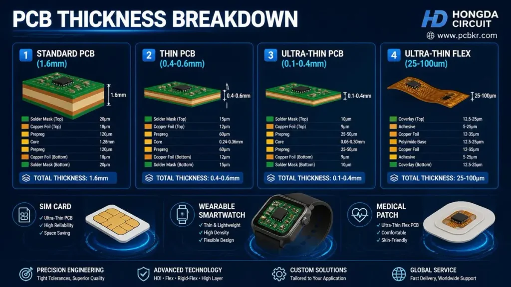
Comprehensive thickness breakdown across standard, thin, ultra-thin rigid, and ultra-thin flex PCBs.
An ultra-thin PCB is a printed circuit board fabricated at a total thickness significantly below the industry-standard 1.6 mm. While definitions vary slightly between fabricators, the consensus in 2026 is:
| Classification | Thickness Range | Typical Use Case |
|---|---|---|
| Standard PCB | 1.0 mm – 2.0 mm | General industrial, consumer electronics |
| Thin PCB | 0.4 mm – 0.6 mm | Smartphones, compact IoT gateways |
| Ultra-Thin PCB | 0.1 mm – 0.4 mm | SIM cards, wearables, medical implants, sensor modules |
| Ultra-Thin Flex | 25 μm – 100 μm | Foldable displays, robotic joints |
The critical distinction is not just the number on the caliper. Ultra-thin PCB fabrication demands specialized handling, thinner copper foils (9–18 μm), modified lamination cycles, and often mSAP (Modified Semi-Additive Process) imaging to hold trace geometry when subtractive etching undercuts become uncontrollable at these scales.
Ultra-Thin Rigid PCB vs. Ultra-Thin Flexible PCB vs. Ultra-Thin Rigid-Flex PCB
- Ultra-Thin Rigid PCB: Built on thinned FR-4 or BT core, retains structural stiffness but at 0.2–0.4 mm. Common in camera modules, LED backlight strips, and NFC antenna carriers.
- Ultra-Thin Flexible PCB (FPC): Uses polyimide (PI) or Liquid Crystal Polymer (LCP) substrates. Can bend repeatedly within a defined radius. Thickness starts at 0.025 mm (25 μm) for single-layer constructions.
- Ultra-Thin Rigid-Flex PCB: Combines rigid islands for component mounting with flexible sections for 3D folding. Medical endoscopes and AR headsets rely on this hybrid format.
At Shenzhen Hongda Circuit Technology, our ultra-thin FPC line routinely produces 0.08 mm flexible circuits, while our rigid ultra-thin program holds ±0.05 mm thickness tolerance down to 0.10 mm single-layer and 0.15 mm double-layer builds.
How Thin Can a PCB Be? Engineering the Thickness Limit
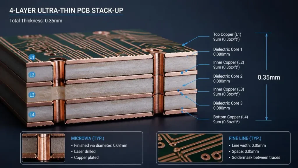
3D micro-section breakdown of a custom 0.35mm 4-layer ultra-thin PCB stack-up featuring 9μm copper foil and laser-drilled microvias.
The theoretical minimum is dictated by physics; review our complete guide on ultra‑thin PCB thickness to understand real‑world production limits for rigid and flexible boards.. For rigid boards, the floor is higher because FR-4 glass weave needs enough resin to prevent fiber breakout during drilling.
Minimum Thickness by Layer Count
| Layer Count | Minimum Achievable Thickness | Manufacturing Notes |
|---|---|---|
| 1-Layer (Single-Sided) | 0.10 mm | Standard for RFID tags, SIM cards |
| 2-Layer (Double-Sided) | 0.15 mm | Requires thinned core, controlled plating |
| 4-Layer | 0.35 mm | Symmetrical stack-up mandatory to prevent warpage |
| 6-Layer | 0.60 mm | High-Tg material recommended; aspect ratio limits apply |
| 8+ Layer Ultra-Thin HDI | 0.80 mm | Any-layer HDI with microvias; mSAP required |
Going below these thresholds is possible, but it triggers exponential cost increases. Below 0.15 mm, panel handling shifts from conveyor systems to vacuum carriers. Below 0.10 mm, you are effectively in substrate-like PCB (SLP) territory, where 8 μm/8 μm line/space and electroplated copper pillars replace conventional etched traces.
Hongda Circuit capability note: Our mSAP line has qualified 8 μm/8 μm line/space for SLP builds, while standard ultra-thin production holds 20 μm/20 μm for smartphone and AI edge applications.
What Types of Ultra-Thin PCBs Are Available?
Not every thin board is built the same way. Your application—whether it is a glucose monitor pressed against skin or a 77 GHz automotive radar module—determines the stack-up architecture.
Ultra-Thin HDI PCB
High-Density Interconnect technology uses microvias (≤0.075 mm), blind/buried vias, and sequential lamination to pack routing into minimal real estate. For ultra-thin HDI, the challenge is maintaining via reliability when the dielectric between layers shrinks to 50 μm or less. We use M9-grade ultra-low loss CCL (Dk < 3.0, Df < 0.005) paired with HVLP5 copper foil to keep signal integrity intact even at 224 Gbps PAM4 data rates.
Ultra-Thin Metal Core PCB
When thinness must coexist with thermal dissipation—think LED backlighting or VCSEL drivers—an aluminum or copper core can be machined down to 0.3 mm. The trade-off is reduced mechanical flexibility and stricter CTE matching during reflow.
Ultra-Thin LED PCB
Mini-LED and micro-LED displays require PCBs that are both thin (0.2–0.4 mm) and thermally conductive. Direct Bonded Copper (DBC) on thin ceramic, or thermally conductive FR-4 with buried metal coins, are the dominant 2026 approaches.
Ultra-Thin Core PCB
Some designs use an ultra-thin core (0.05–0.10 mm) as the central spine of a multilayer build, surrounded by thinner prepregs. This technique is common in high-layer-count server boards where overall thickness must stay under 1.0 mm despite 20+ layers.
Which Materials Are Used for Ultra-Thin PCBs?
Material selection is where most ultra-thin PCB projects succeed or fail. A substrate that works at 1.6 mm may delaminate, warp, or fracture when thinned to 0.2 mm.
FR-4 and High-Tg FR-4 for Ultra-Thin Rigid PCB
Standard FR-4 can be sourced in thinned cores down to 0.05 mm. However, for lead-free assembly (peak reflow 245–260 °C), High-Tg (≥170 °C) or Mid-Tg variants prevent resin softening and subsequent bow. At Hongda Circuit, we stock Isola 185HR and Panasonic M6/M7 for thin-core applications.
Polyimide and LCP for Ultra-Thin Flexible PCB
- Polyimide (PI): The workhorse of flex circuits. Tg > 300 °C, excellent chemical resistance, but absorbs moisture (pre-bake required before assembly).
- Liquid Crystal Polymer (LCP): Lower moisture absorption than PI, superior high-frequency performance (Dk ~ 2.9 @ 10 GHz), and ideal for 5G mmWave antennas in ultra-thin form factors.
Ultra-Thin Copper Foil
The global ultra-thin copper foil market was valued at $2.082 billion in 2025 and is projected to reach $5.007 billion by 2034, growing at a CAGR of 13.5%. This growth is driven by the shift toward miniaturized, high-performance PCBs in 5G infrastructure, AI servers, and electric vehicles.
For ultra-thin PCB fabrication, we specify:
- HTE (High-Temperature Elongation) foil: 12 μm or 9 μm for standard traces.
- HVLP (Hyper-Very-Low-Profile) foil: 3–5 μm for mSAP processing; reduces skin effect losses at RF frequencies.
Low-Loss and Ultra-Low-Loss Laminates
As data rates climb, even thin boards must manage insertion loss. Our 2026 material ecosystem includes:
- Megtron 7 / Megtron 8 (Panasonic)
- Tachyon 100G (Isola)
- RO4350B / RT5880 (Rogers)
- M9-grade CCL for AI server and 6G communication hardware
What Manufacturing Challenges Do Ultra-Thin PCBs Have?

Automated mSAP fine-line processing and laser inspection system ensuring ±0.05mm warpage tolerance on ultra-thin PCB panels.
If your current supplier treats a 0.2 mm board like a scaled-down 1.6 mm board, you will see yield loss, warpage, and intermittent opens. Here are the real challenges—and how a qualified ultra-thin PCB manufacturer solves them.
Warpage and Bow Control
Board warpage is the #1 killer of ultra-thin yields. Copper has a CTE of ~17 ppm/°C; FR-4 z-axis CTE is 45–55 ppm/°C. During reflow, that mismatch creates stress that releases as bow or twist. For boards under 0.6 mm, IPC-6012 allows ≤0.75% warpage for SMT—but achieving it requires:
- Symmetric stack-ups: Mirror copper weights, core thickness, and prepreg about the board centerline.
- Balanced copper distribution: Use copper thieving and dummy fills on sparse layers.
- Controlled lamination: Vacuum lamination with gradual heating and cooling profiles.
At Hongda Circuit, our LAUFFER lamination system uses zone-controlled pressure and temperature ramps to keep thin panels flat within ±0.05 mm.
Handling and Panelization
A 0.15 mm panel cannot ride a standard conveyor. It sags, creases, or slips. We use:
- Vacuum carrier fixtures during imaging and etching.
- Tab-routing with support rails instead of V-scoring for fragile outlines.
- Reduced stack heights during drilling (max 2–3 panels vs. 6+ for standard boards).
Microvia Drilling and Registration
In ultra-thin HDI, dielectric layers may be only 25–40 μm thick. Laser drilling must achieve ≤0.05 mm blind vias without punching through to the next layer. Our Mitsubishi UV/CO₂ laser drilling system holds ±5 μm positional accuracy, and layer-to-layer registration is maintained within ±10 μm using automated optical alignment.
Etching Uniformity and mSAP
Subtractive etching of 9 μm foil on a 0.2 mm board is a recipe for over-etching and trace necking. That is why we migrated critical ultra-thin jobs to mSAP:
- Laminate 1.5–3 μm ultra-thin copper seed layer.
- Image with SCREEN Ledia LDI at ±1.5 μm accuracy.
- Selectively plate copper to target height (15–20 μm).
- Flash-etch the seed layer.
Result: near-vertical trace sidewalls, minimal undercut, and impedance control within ±5% across the panel.
Surface Finish Selection for Thin Profiles
- ENIG (Electroless Nickel Immersion Gold): Flat, oxidation-resistant, ideal for fine-pitch BGAs. We run both standard (2–4 μin gold) and thin-ENIG (1.5–2.0 μin) for high-frequency applications.
- OSP (Organic Solderability Preservative): Ultra-thin (<0.5 μm), preserves board thickness, but limited shelf life.
- ENEPIG: Excellent for aluminum wire bonding in medical sensor modules.
Our ENIG line includes XRF spectrometers calibrated weekly to NIST-traceable standards, ensuring nickel and gold thickness never drift out of spec.
2026 Ultra-Thin PCB Manufacturing Technology Trends
The ultra-thin PCB landscape is evolving rapidly. Here is what is changing on the factory floor this year—and what it means for your next design.
LDI and mSAP Become Standard for Fine-Line Ultra-Thin PCB Fabrication
Laser Direct Imaging (LDI) has replaced film-based photolithography in most advanced shops. It eliminates phototool degradation, improves layer-to-layer alignment, and supports sub-50 μm trace resolution. Combined with mSAP, fabricators can now mass-produce 15–30 μm line/space on 0.2 mm cores—something impossible with subtractive etching alone.
AI-Driven Process Control and Digital Twins
Leading manufacturers now deploy AI-driven AOI and digital twin simulations to predict thermal behavior before the first panel is laminated. At Hongda Circuit, our AI-driven ERP tracking system monitors every job in real time, contributing to an on-time delivery rate exceeding 95%.
M9-Grade Laminates Enter Mass Production
2026 marks the first year of large-scale mass production for M9-grade copper-clad laminates, driven by NVIDIA Rubin/VR300 platforms and 224 Gbps signaling. These materials feature:
- Df ≤ 0.0005–0.0008 @ 10 GHz
- Tg ≥ 200 °C
- Dk 2.8–3.0 @ 10 GHz
For ultra-thin designs that must also handle high-speed signals, M9-grade CCL is becoming the default.Sustainable Ultra-Thin PCB Manufacturing
Environmental regulations are pushing the industry toward halogen-free laminates, lead-free finishes, and closed-loop etchant recycling. Hongda Circuit maintains RoHS-compliant processes and offers halogen-free material options for medical and automotive clients who need full material declaration (FMD) documentation.
How Much Does an Ultra-Thin PCB Cost?
There is no fixed price list. Ultra-thin PCB cost depends on a matrix of interlocking variables:
| Cost Driver | Impact on Price |
|---|---|
| Thickness | Below 0.2 mm, handling complexity increases exponentially. |
| Layer count | Each additional layer requires another lamination cycle, raising warpage risk. |
| Line/space | Below 50 μm requires LDI + mSAP; below 30 μm requires SLP-grade equipment. |
| Material grade | M9 CCL or LCP costs 3–5× standard FR-4. |
| Microvia density | Stacked microvias need sequential lamination and filled-via plating. |
| Surface finish | ENEPIG > ENIG > OSP in cost. |
| Testing | 100% AOI + X-ray + flying probe adds 10–20% but prevents field failures. |
| Volume | Prototype lots (5–10 pcs) have high NRE; 1,000+ panels amortize tooling. |
Getting an Accurate Ultra-Thin PCB Quote
The fastest way to receive a precise ultra-thin PCB quote is to provide:
- Gerber files and drill files.
- Stack-up drawing or target impedance requirements.
- Material specification (or let our engineers recommend).
- Quantity and delivery timeline.
At Hongda Circuit, we provide 30-minute inquiry response and 1-hour engineering evaluation for all ultra-thin PCB RFQ submissions. No generic calculators—every quote is reviewed by a process engineer who checks manufacturability before you commit to tooling. Email:pcb@pcbkr.com
Which Industries Use Ultra-Thin PCBs?
The global medical PCB board market is projected to reach $14.2 billion by 2034, expanding at a CAGR of 7.5%. Within that, the wearable devices segment is the fastest-growing at 11.4% CAGR, fueled by continuous glucose monitors, cardiac loop recorders, and smart patches. Ultra-thin PCBs are the enabler.
Wearable Electronics and Medical Devices
- Continuous glucose monitors (CGMs): 0.2 mm rigid-flex with exposed PI flex for skin contact.
- Hearing aids: 0.15 mm multilayer with microvias and ENIG for chip-on-board (COB) assembly.
- Smart patches: Ultra-thin FPC (0.08 mm) with stretchable conductive ink traces.
Consumer Electronics and Mobile Devices
Foldable smartphones, ultra-slim laptops, and TWS earbuds all rely on ultra-thin rigid or rigid-flex PCBs to maximize battery volume. A 0.1 mm reduction in PCB thickness can translate to 200+ mAh of additional battery capacity.
Automotive and ADAS
Automotive radar modules, camera-based driver-assistance systems, and interior touch surfaces use ultra-thin PCBs to fit behind curved dashboards. These applications demand IATF 16949 certification and thermal cycling reliability beyond 1,000 cycles.
IoT, Sensors, and Industrial Electronics
Smart labels, NFC payment cards, and industrial vibration sensors use ultra-thin form factors to embed electronics into spaces previously considered impossible.
How Do You Choose an Ultra-Thin PCB Manufacturer?
Not every PCB shop that advertises “thin boards” has the equipment, process control, or quality system to deliver repeatable results. Use this checklist when evaluating an ultra-thin PCB supplier:
Verify Equipment and Process Depth
- Do they own LDI imaging in-house, or outsource to a third party?
- Is mSAP or SAP available for fine-line work?
- Can they handle Any-Layer HDI with stacked microvias?
- Do they have vacuum lamination with pressure profiling?
Inspect Quality Certifications
- ISO 9001:2026 — baseline quality management.
- IATF 16949 — mandatory for automotive.
- AS9100D — required for aerospace and defense.
- ISO 13485 — essential for medical device manufacturing.
- IPC-6012 Class 3 / 3A — high-reliability acceptance criteria.
Evaluate Engineering Support
A true partner reviews your stack-up before tooling begins. Ask:
- Will they perform a DFM review and flag copper imbalance or via aspect ratio risks?
- Can they simulate impedance and thermal profiles?
- Do they offer 24-hour technical support during prototype debug?
Assess Supply Chain and Delivery Performance
- What is their on-time delivery rate?
- Do they stock next-gen materials (M9, Megtron 8, LCP) or special-order everything?
- Can they support rapid prototyping (5-day turnaround) alongside volume production?
Why Shenzhen Hongda Circuit Technology Co., Ltd. Is Your Trusted Ultra-Thin PCB Partner
Shenzhen Hongda Circuit Technology Co., Ltd. has been manufacturing precision interconnects since 1999. Our Baoan, Shenzhen facility is not a broker or trading house—we own every critical process step in-house.
Proven Ultra-Thin PCB Manufacturing Capabilities
| Specification | Mass Production | Sample / Prototype |
|---|---|---|
| Min. Thickness (Rigid) | 0.15 mm (2L) | 0.10 mm (1L) |
| Min. Thickness (Flex) | 0.08 mm | 0.05 mm |
| Max. Layer Count | 28 layers | 78 layers |
| Min. Trace/Space | 1.8 mil / 1.8 mil (45 μm) | 1.0 mil / 1.0 mil (25 μm) |
| Microvia Diameter | Blind 0.05 mm / Buried 0.15 mm | Blind 0.02 mm / Buried 0.08 mm |
| HDI Order | 6+N+6 Any-Layer | 7-order HDI |
| High-Speed Signaling | 224 Gbps PAM4 | 112 Gbps+ backplanes |
Advanced Equipment Portfolio
- SCREEN Ledia LDI — direct imaging for soldermask and etch resist, eliminating phototool variation.
- Mitsubishi UV/CO₂ Laser Drilling — microvia formation down to 0.075 mm.
- LAUFFER Lamination System — zone-controlled pressure for thin-panel flatness.
- Nordson DAGE X-Ray — 3D void detection in PTH and microvias.
- XRF Spectrometers — non-destructive gold/nickel thickness verification.
- Multi-chamber inline PVD — for ceramic substrate and thin-film metallization.
Certifications That Matter
- ISO 9001:2026
- AS9100D (Aerospace)
- IATF 16949 (Automotive)
- IPC-6012 Class 3 / 3A
- ISO 13485 (Medical Device — dedicated production lanes available)
Material Ecosystem and Speed
We maintain strategic inventory of M9-grade CCL, Megtron 7/8, RO4350B, RT5880, and LCP, sourced directly from Isola, Panasonic, Rogers, and Taconic. Our AI-driven ERP tracks every order in real time, and our engineering team guarantees 30-minute RFQ response, 1-hour DFM evaluation, and 24-hour technical support.
Ultra-Thin PCB FAQ — What Procurement Teams Ask Before Sourcing
What is the minimum thickness you can manufacture for a multilayer ultra-thin PCB?
For mass production, we reliably fabricate 4-layer ultra-thin PCBs at 0.35 mm and 6-layer at 0.60 mm while maintaining IPC-6012 Class 3 flatness. For prototypes, we have delivered 2-layer boards at 0.15 mm and single-layer at 0.10 mm. Below 0.20 mm, we switch to vacuum-carrier handling and mSAP imaging to protect trace integrity.
How do you control warpage on ultra-thin PCBs during reflow assembly?
We attack warpage at three stages. Design stage: Our DFM team verifies copper balance and stack-up symmetry. Fabrication stage: LAUFFER vacuum lamination with gradual thermal ramps and post-etch baking removes residual stress. Delivery stage: We ship thin boards in rigid support frames and recommend carrier fixtures for your SMT line. For critical jobs, we can supply flatness measurement data per IPC-TM-650 Method 2.4.22.
Can you manufacture ultra-thin PCBs with controlled impedance for high-speed signals?
Yes. Impedance control on thin substrates is actually more sensitive because dielectric thickness directly affects Zo. A 5 μm variation in trace width can shift impedance by 2–3 Ω—unacceptable for 224 Gbps channels. We use mSAP for near-vertical trace profiles, LDI for ±1.5 μm imaging accuracy, and Polar impedance testing on every coupon. Target tolerances are typically ±5% for ultra-thin high-speed designs.
What is the typical lead time for ultra-thin PCB prototypes vs. volume production?
Prototypes (5–50 pcs): 5–7 working days for 2–4 layer; 10–12 days for HDI or rigid-flex.
Volume (1,000+ panels): 2–3 weeks for standard ultra-thin; 4–5 weeks for Any-Layer HDI with M9 materials.
Expedited lanes are available for medical and automotive emergency builds. Contact sales@pcbkr.com with your Gerbers for a locked schedule.
How do I know if my design needs a ultra-thin rigid PCB or an ultra-thin flexible PCB?
If your product requires static bending during installation only (e.g., a camera module flexing once into a housing), a rigid ultra-thin PCB at 0.2–0.4 mm is usually sufficient and more cost-effective. If the circuit must dynamically flex repeatedly—wearables, foldable phones, robotic joints—you need a polyimide-based ultra-thin flexible PCB or a rigid-flex hybrid. Send us your mechanical envelope and bend-cycle requirements; our engineers will recommend the stack-up and material set that balances performance, reliability, and unit cost.
Ready to Source Your Ultra-Thin PCB? Start With a DFM Review.
Thin boards demand thick expertise. Whether you need a 0.08 mm flex circuit for a biometric patch or a 0.35 mm 4-layer HDI for a foldable phone hinge, the margin for error is measured in microns. Shenzhen Hongda Circuit Technology Co., Ltd. combines mSAP fine-line processing, Any-Layer HDI, M9-grade materials, and ISO-certified quality systems to deliver ultra-thin PCBs that survive assembly, reflow, and years of field use.
Next step: Email your Gerbers and stack-up requirements to sales@pcbkr.com. Our engineering team will return a manufacturability review and firm quote within 24 hours.
About Author
David Chen https://www.linkedin.com/in/pcbcoming
David Chen boasts an extensive professional background in PCBA manufacturing, PCBA testing, and PCBA optimization, with specialized expertise in high-precision PCBA fault analysis and rigorous PCBA reliability testing. The author has worked with high-layer-count server PCB fabrication, ultra-low-loss backplane stackups, and thermo-mechanical reliability optimization for AI infrastructure projects involving 112G and 224G PAM4 architectures. Skilled in complex circuit design and cutting-edge advanced PCB manufacturing processes, he delivers solutions that elevate product durability and performance across industrial applications. His technical articles focusing on PCBA manufacturing workflows and testing methodologies are widely cited by industry peers, research institutions, and technical platforms, solidifying his reputation as a recognized technical authority in the global circuit board manufacturing sector.