Why HDI PCBs Are Chosen for AI Servers?
AI servers demand High-Density Interconnect (HDI) PCBs because traditional through-hole architectures cause catastrophic signal degradation above 56Gbps/112Gbps PAM4 and cannot route tight ≤0.4mm BGA pitches. HDI eliminates these limits through laser-drilled microvias, ultra-low-loss structures, and stacked architectures, delivering unparalleled signal integrity, space optimization, thermal relief, and stable power routing.
Why Do AI Servers Require Any-Layer HDI Rather Than Traditional Multilayer Boards?
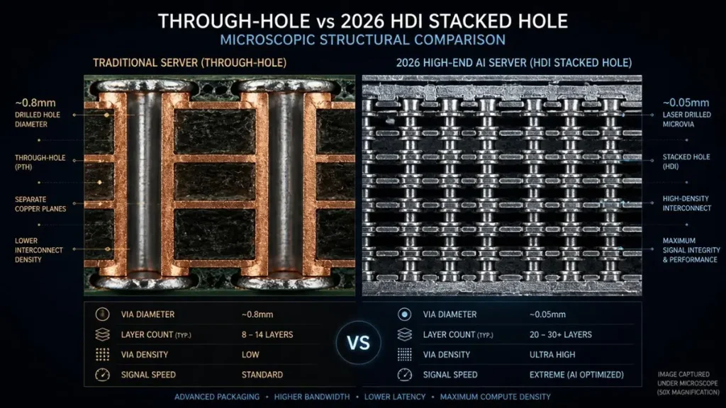
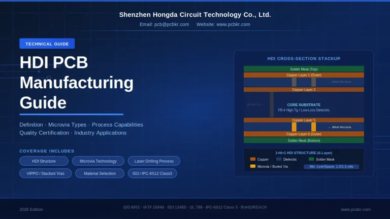
Advanced HDI PCB Via Configurations and Microscopic Cross-Section View
Direct Answer: Traditional multilayer PCBs rely on mechanical through-holes that form resonant capacitive stubs, destroying 112G PAM4 signals. Any-layer HDI replaces them with stacked, copper-filled microvias, removing stubs completely and providing a 30% reduction in insertion loss and a 45% reduction in cross-delay.
At Shenzhen Hongda Circuit Technology Co., Ltd., our deployment of 2026-generation ultra-HDI (UHDI) manufacturing proves that signal transmission at frequencies exceeding 28 GHz cannot tolerate the parasitic capacitance of standard vias. The capacitance of a via is governed by the formula:
C = (1.41 * εr * T * D1) / (D2 – D1)
Where εr is the material permittivity, T is substrate thickness, D1 is via diameter, and D2 is anti-pad diameter. By shrinking D1 from 250μm mechanical drills to ≤75μm laser microvias, the parasitic capacitance drops by over 70%, completely suppressing signal reflections.
Furthermore, the quarter-wave resonance frequency (fresonance) introduced by standard via stubs is computed via:
fresonance = c / (4 * Lstub * √εr)
Where c is the speed of light and Lstub is the length of the via stub. In a traditional 24-layer server board with back-drilling tolerances of ±5 mils, a remnant stub of 10 mils notches out signals near 56 GHz, which directly curtails the fundamental frequency of 112G PAM4 signaling. Any-layer HDI utilizes an Embedded Light Interconnect Construction (ELIC) where sequential lamination eliminates the physical existence of stubs, ensuring an unattenuated transmission path up to 70 GHz.
Detailed Manufacturing Pain Point: Microvia Interfacial Voiding & Target Alignment
When executing 5-6 step sequential laminations for 24-layer AI server boards, a critical vulnerability is the microvia-to-target-pad interface. During the electroplating process, gas entrapment or inadequate chemical mass transfer inside a 75μm blind hole causes sub-micron voids. Under the intense thermal stress of an OAM module operating at 105°C, these voids propagate due to Coefficient of Thermal Expansion (CTE) mismatch, leading to latent open circuits. Hongda solves this by utilizing vacuum-assisted horizontal pulse plating and strict ≤35μm layer-to-layer registration accuracy managed by computerized Laser Direct Imaging (LDI).
Expert Engineering Insight from Hongda Field Application Team:
“When routing the PCIe 6.0 interface on an AI Accelerator board, engineers often overlook the via stub effect. A stub as short as 15 mils acts as a quarter-wave resonator that notches out the 56 GHz fundamental frequency. Moving to an any-layer stacked microvia configuration removes the stub entirely. Our lab verification shows that insertion loss drops from 0.72 dB/inch to 0.41 dB/inch at 28 GHz when switching from back-drilled through-holes to an ELIC structure.”
How Do HDI PCB Advantages Solve the 0.355mm BGA Pitch Routing Crisis in Next-Gen AI Substrates?
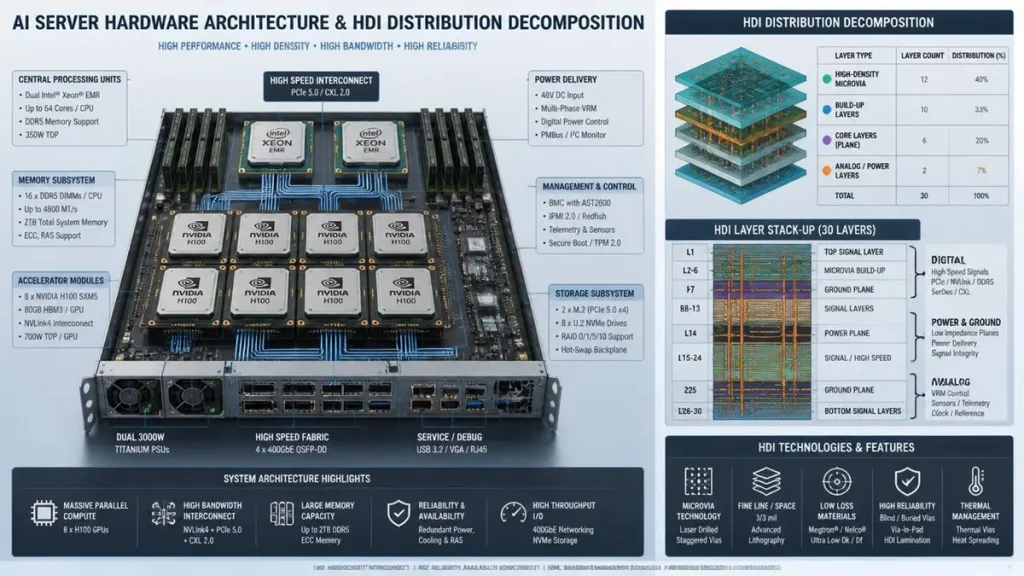
I Server Hardware Architecture & HDI PCB Distribution Exploded View
Direct Answer: Next-generation GPU and HBM3e architectures utilize a 0.355mm BGA pitch, which makes breakout routing physically impossible with mechanical vias. HDI solves this crisis by embedding microvias directly within BGA pads (Via-in-Pad/VIPPO) and shrinking track/space geometries to ≤1.8 mil (45μm), unlocking over 40% space savings.
Detailed Application Scenario: GPU to HBM3e Interconnect
Consider an AI accelerator module containing a high-performance GPU tightly clustered with eight HBM3e stacks. The escape routing requires thousands of high-speed interconnect lines packed into a localized area. Standard routing rules fail because a 0.2mm mechanical drill plus land pad takes up ≥0.45mm of space, which is wider than the entire pitch interval of 0.355mm.
Our 2026 tech stack utilizes Modified Semi-Additive Process (mSAP) to achieve 45μm line widths and spacings. This allows two lines to be routed safely between BGA pads, preventing cross-talk through coplanar waveguide shielding structures. By substituting traditional subtractive copper etching with additive electrolytic plating into precise dry-film photoresist patterns, the etch factor is raised from a standard 3.0 to ≥5.0, achieving near-perfect rectangular conductor cross-sections.
| Routing Metric | Traditional Pitch Routing (0.8mm) | 2026 AI HDI Substrate (0.355mm) | Hongda Production Capability Threshold |
|---|---|---|---|
| Line Width / Space | 4.0 / 4.0 mil (100μm) | 1.8 / 1.8 mil (45μm) | 1.5 / 1.5 mil (38μm) ±10% |
| Via Pad Diameter | 18 mil (450μm) | 8 mil (200μm) | 6.5 mil (165μm) |
| Drill Technology | Mechanical (≥200μm) | UV/CO2 Hybrid Laser (≤75μm) | Femtosecond Laser (≤50μm) |
| Aspect Ratio | 10:1 | 1:1 (Microvia) | 1.2:1 (Advanced Filling) |
How Does High-Order HDI Mitigate Thermal Stress and Power Supply Ripple in 1000W+ AI Accelerators?
Direct Answer: High-order HDI uses copper-filled stacked blind vias and ultra-thin, high-thermal-conductivity dielectrics to create direct thermal-electrical paths. This suppresses power supply ripple to ≤15mV (below the strict 20mV ASIC threshold) and channels localized heat away from 100W/cm² GPU cores.
Modern AI server chips pull transient currents that spike from 10A to 1200A in nanoseconds. The Target Impedance (Ztarget) and Loop Inductance (L) of the Power Distribution Network (PDN) must be minimized according to the voltage drop equation:
ΔV = L * (di / dt)
By placing stacked microvias directly inside the capacitor landing pads (Via-in-Pad) on the reverse side of the GPU, Shenzhen Hongda Circuit Technology Co., Ltd. minimizes the current loop path. This architecture eliminates the equivalent series inductance (ESL) associated with long surface traces, ensuring power supply voltage remains completely stable under peak computing loads.
Furthermore, thermal dissipation is heavily optimized. Glass-backed hydrocarbons or advanced resin systems exhibit poor thermal conductivity (k ≈ 0.35 W/m·K). By designing solid copper-filled stacked microvias from Layer 1 through Layer 6 directly beneath the silicon die attachment point, we create solid metallic heat conduits (k ≈ 398 W/m·K). This routes localized heat fluxes directly into internal heavy copper planes, reducing the junction temperature (Tj) of processing units by up to 12°C.
Detailed Manufacturing Pain Point: VIPPO Outgassing & Planarity Failures
A persistent failure mode in ultra-dense boards is outgassing within Via-in-Pad Plated Over (VIPPO) structures. If the epoxy resin plug inside the blind via contains microscopic volatile organic solvents, these expand violently during the 260°C lead-free reflow profile. This pushes up the copper capping layer, creating a microscopic protrusion. A protrusion of just 8μm prevents uniform solder paste transfer for 0.4mm BGAs, causing head-in-pillow (HiP) solder defects. Hongda utilizes 100% solvent-free ceramic-filled thermocompression resins and chemical-mechanical planarization (CMP) to guarantee a surface coplanarity of ≤5μm.
Find Out About Us: Delivering Top-Tier Fabrication for Both AI & Conventional PCBs
Navigating the line between cutting-edge innovation and high-volume, cost-effective production shouldn’t be a compromise. At Shenzhen Hongda Circuit Technology (PCBKR), we bridge this gap by elevating the manufacturing standards for both high-performance AI hardware and traditional multi-layer PCBs.
By integrating advanced manufacturing methodologies across all production lines, we bring an elite level of precision to traditional PCB fabrication. Our standard boards benefit from enhanced interlayer alignment tolerances (down from ±75μm to within ±25μm) and tightened differential impedance control (±5%). Supported by 100% 3D X-Ray (AXI) inspection, your conventional boards achieve chip-level reliability, superb signal stability, and near-100% yield.
Your Strategic Manufacturing Partner
We proudly stand as a dual-capability partner: offering the elite technical ceiling required for next-gen AI hardware, while maintaining the exceptional flexibility, rapid turnaround, and unmatched cost-efficiency needed for mid-to-high-volume traditional board campaigns. You get zero-defect reliability without the premium overhead or bureaucracy of massive tier-1 factories.
Ready to upgrade your hardware’s reliability?
Submit your Gerber files today for an agile engineering review and a highly competitive quote.
Contact our experts: sales@pcbkr.com
FAQ: Mastering HDI PCB AI Server Advantages
What is the fundamental difference in cost-performance ratio between 2-step HDI and Any-Layer ELIC for AI servers?
While 2-step HDI (conventional 2+N+2 build-up) is sufficient for simple PCIe riser cards, it requires stagger-step patterns that consume horizontal routing space. Any-layer ELIC allows infinite vertical stacking of copper-filled microvias, enabling 0.355mm BGA escapes. Though ELIC carries a 35% processing premium over 2-step HDI due to repetitive sequential laminations, it reduces layer count requirements by up to 20% and guarantees zero signal stubbing at 112G PAM4 speeds.
How does Hongda’s 2026 mSAP technology compare to traditional subtractive etching in signal integrity preservation?
Traditional subtractive etching creates a trapezoidal trace cross-section due to chemical undercut, causing an unpredictable skin effect at high frequencies. Hongda’s 2026 Modified Semi-Additive Process (mSAP) electroplates copper into photoresist channels, delivering near-vertical rectangular trace walls (etch factor ≥5.0). This provides precise ±5% impedance control and limits differential phase skew to ≤1.2 ps/inch, which is essential for error-free 224Gbps PAM4 optical engine transitions.
Why do standard high-speed FR4 materials fail in AI server HDI stacks compared to Ultra-Low-Loss substrates?
Standard FR4 materials feature a Dissipation Factor (Df) of 0.015 to 0.020, converting critical high-frequency signal energy into dielectric heat. AI server HDI architectures require Ultra-Low-Loss substrates (e.g., Tachyon 100G or Megtron 7) with a Df of ≤0.0015 and a Dielectric Constant (Dk) of ≤3.2. Combined with Any-Layer HDI’s short microvia lengths, these materials compress total insertion loss to just 0.38 dB/inch at 28 GHz, preventing signal attenuation over lengthy multi-board routing channels.
How do stacked microvias and staggered microvias contrast in terms of thermal reliability and routing efficiency?
Stacked microvias are positioned directly on top of each other, providing the ultimate routing efficiency and shortest power paths but generating severe localized thermal stress concentration at the copper interfaces. Staggered microvias offset each layer’s via, dispersing CTE-driven stress and offering higher thermal reliability across 1,000 thermal cycles (-40°C to +125°C), but they consume valuable horizontal routing lane real estate. For 2026 AI designs, Hongda uses advanced pulse plating to ensure stacked microvias achieve identical reliability ratings to staggered configurations.
How does Via-in-Pad Plated Over (VIPPO) solve the specific problem of power rail loop inductance compared to external dogbone via connections?
Traditional dogbone routing links a BGA pad to a nearby via through a short surface trace, creating an external loop path that adds up to 120 pH of parasitic loop inductance. VIPPO drops the microvia vertically straight down through the pad directly into internal power or ground planes, reducing loop inductance to less than 15 pH. This instantaneous charge delivery suppresses power plane bounce and keeps transient noise well within the ≤15mV limit required by high-power GPUs.
About Author
David Chen https://www.linkedin.com/in/pcbcoming
David Chen boasts an extensive professional background in PCBA manufacturing, PCBA testing, and PCBA optimization, with specialized expertise in high-precision PCBA fault analysis and rigorous PCBA reliability testing. The author has worked with high-layer-count server PCB fabrication, ultra-low-loss backplane stackups, and thermo-mechanical reliability optimization for AI infrastructure projects involving 112G and 224G PAM4 architectures. Skilled in complex circuit design and cutting-edge advanced PCB manufacturing processes, he delivers solutions that elevate product durability and performance across industrial applications. His technical articles focusing on PCBA manufacturing workflows and testing methodologies are widely cited by industry peers, research institutions, and technical platforms, solidifying his reputation as a recognized technical authority in the global circuit board manufacturing sector.