Metal Core PCB: Engineering Guide to MCPCB Design, Manufacturing, and Thermal Management in 2026
A metal core PCB — also referred to as an MCPCB, aluminum PCB, or metal core printed circuit board — is a substrate in which the conventional FR-4 glass-epoxy base is replaced by a thermally conductive metal layer, most commonly aluminum alloy. The substitution is not cosmetic. In applications where power density exceeds roughly 5 W/cm², a standard FR-4 board accumulates heat faster than convection or airflow can remove it, creating localized hot zones that degrade junction temperature, accelerate solder fatigue, and shorten device lifespan. Metal core PCB technology addresses this by providing a direct thermal conduction path from the component to a heat-spreading substrate, bypassing the insulating bottleneck of polymer-glass laminates entirely.
This guide covers the engineering fundamentals, material selection logic, layer structure, manufacturing process constraints, failure modes, and procurement criteria for metal core PCBs and aluminium core PCBs. The content reflects process capability updates through 2026, including advances in low-thermal-resistance dielectric bonding and high-density MCPCB fabrication.
Why FR-4 Fails in High-Power Applications — The Thermal Problem Metal Core PCB Solves
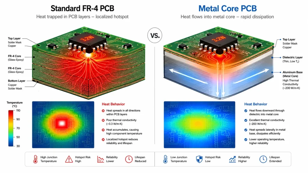
Engineering comparison of thermal dissipation mechanisms and hotspot formation between Standard FR-4 PCB (left) and Aluminum Metal Core PCB (right) under an identical 3.2W component load.
FR-4 laminate has a through-plane thermal conductivity of approximately 0.3 W/m·K. That number is adequate for signal-level electronics where power dissipation per unit area is low. Once a board carries high-current power stages, dense LED arrays, or switching converters with devices dissipating more than 1 W each at tight pitch, the math changes quickly.
Consider a power LED cluster running 50 W across a 20 × 20 mm footprint. With FR-4 at 0.3 W/m·K and a 1.6 mm board thickness, the thermal resistance from copper pad to the back of the board is roughly 27 K/W. A metal core PCB using a 1.5 W/m·K dielectric layer drops that same figure to around 5–6 K/W — a 4× to 5× improvement before any heatsink is attached. The practical consequence is a junction temperature 60–80°C lower at the same ambient, which directly translates to longer LED lumen maintenance, reduced driver derating, and fewer thermal-stress-induced solder joint failures.
Beyond steady-state temperature, the issue is thermal cycling fatigue. When FR-4 boards heat and cool in service, the large CTE mismatch between copper (17 ppm/K) and the polymer matrix (50–70 ppm/K in-plane) drives micro-crack propagation at via barrels and pad interfaces. Aluminum substrate has a CTE of roughly 23 ppm/K — closer to copper — and its high thermal mass damps the temperature swing amplitude, reducing the cyclic strain range imposed on solder joints. This matters in automotive and industrial environments where daily temperature excursions of 40–100°C are routine.
Typical Failure Indicators That Suggest Switching to MCPCB
- Junction temperature exceeds rated Tj by more than 15°C under normal operating load
- Solder joint cracking appears within 500–1,000 thermal cycles in qualification testing
- Board warpage exceeds IPC-A-610 limits during reflow due to thermal gradient across the panel
- LED flux drops more than 30% within 5,000 hours of operation
- Dielectric breakdown or leakage current appears on high-voltage power boards after thermal aging
Metal Core PCB Layer Structure: Copper, Dielectric, and Substrate
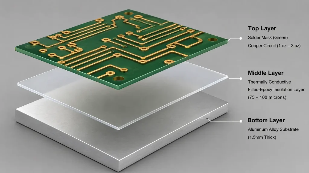
3D isometric exploded view of a standard single-layer Aluminum MCPCB stackup, demonstrating the spatial relationship between the top copper circuit, the 75–100 µm thermal dielectric, and the 1.5mm aluminum core substrate.
A standard single-layer MCPCB consists of three functionally distinct layers. Understanding each layer’s role is necessary for making sound design decisions, because the thermal and electrical performance of the finished board is determined largely by the dielectric interlayer — not the metal substrate itself.
Copper Circuit Layer
The top copper layer carries the circuit traces and component pads. Thickness ranges from 1 oz (35 µm) for signal-level circuits to 3 oz or 4 oz (105–140 µm) for high-current power paths. Thicker copper lowers trace resistance and spreads heat laterally before it reaches the dielectric, but it also increases the difficulty of fine-pitch etching and raises peel-force requirements for the copper-to-dielectric bond. In 2026, high-density MCPCB designs with 3/3 mil (76/76 µm) trace/space capability and 1 oz copper are in volume production; achieving that resolution with 2 oz copper requires tighter etch process control and specialized dielectric surface preparation.
Thermal Dielectric Layer (Insulation Layer)
This is the most technically critical layer in any aluminum PCB or metal core printed circuit board. It must simultaneously provide electrical isolation — typically 1,000 V AC minimum, often 3,000 V AC for industrial designs — and the lowest possible thermal resistance between the copper and the metal substrate. These two requirements are in direct tension: thinner dielectrics conduct heat better but reduce creepage distance and breakdown voltage margins.
Standard filled-epoxy dielectric (such as the widely used 7628 prepreg variant modified with boron nitride or aluminum oxide fillers) achieves 1.0–2.0 W/m·K at thicknesses of 75–100 µm. Advanced ceramic-filled PTFE or polyimide-based dielectrics available in 2026 reach 3.0–6.0 W/m·K but cost 3× to 5× more and require modified lamination parameters. The dielectric thickness specification is one of the first decisions to nail down in a new aluminium core PCB design — it sets the ceiling on achievable thermal performance and influences the voltage rating, registration tolerance, and pad-to-metal clearance requirements simultaneously.
Metal Substrate (Core Layer)
For the majority of aluminum PCB designs, the substrate is a 1.0–3.0 mm aluminum alloy plate, most commonly 5052-H32 or 6061-T6. Both alloys have bulk thermal conductivity of 130–170 W/m·K and offer excellent machinability and surface flatness after anodization or chromate conversion pre-treatment. Copper-core MCPCBs using C11000 oxygen-free copper (thermal conductivity ~390 W/m·K) are used in extreme-performance RF or power applications where every degree matters, but the 3× material cost and the need for nickel barrier plating before surface treatment restrict copper-core usage to specialized designs. Steel-core MCPCBs appear in applications requiring magnetic shielding or where EMC enclosure integration is the primary goal; their thermal conductivity (14–20 W/m·K) makes them thermally inferior to aluminum variants.
Metal Substrate Selection for MCPCB: Aluminum vs. Copper vs. Steel
Selecting the substrate material for a metal core PCB involves weighing thermal performance, weight, machinability, CTE compatibility with mounted components, and unit cost at the target production volume. No single material is universally optimal; the right choice depends on the specific thermal budget and mechanical envelope of the design.
Aluminum Core PCB (Most Common Choice)
Aluminum substrate dominates the market for a straightforward reason: it delivers a thermal conductivity of 130–170 W/m·K at a material cost roughly 4× lower than copper and with far better manufacturability. Aluminum plates can be drilled, routed, and punched with carbide tooling at high throughput; their relatively low hardness compared to copper reduces tool wear per unit panel area. Anodization of the exposed back surface after board fabrication creates a 5–25 µm hard oxide layer that improves corrosion resistance and, in some cases, provides additional electrical isolation to the heatsink mounting surface. The aluminium core PCB (using the British spelling) is the same product — the label difference is geographic, not technical, and any reputable MCPCB supplier should recognize both spellings without ambiguity.
Copper Core PCB
Copper substrate at 380–400 W/m·K is the choice when aluminum’s thermal performance is genuinely insufficient — typically in GaN power modules, high-brightness laser diode arrays, or microwave power amplifiers operating above 50 W in confined housings. The practical constraints are significant: copper is 3.3× denser than aluminum (adding weight), the CTE of 17 ppm/K matches ceramic components better but requires careful dielectric selection to avoid delamination, and cutting or drilling copper core boards accelerates tool wear markedly. Plating adhesion on copper substrate also requires nickel underplating before tin-lead or ENIG surface finish, adding a process step.
Steel Core PCB
Steel substrate is specified where magnetic or EMC properties take precedence over thermal management. Stainless steel (14–16 W/m·K) and mild steel (45–50 W/m·K) both conduct heat far less effectively than aluminum, so steel-core MCPCBs are not a viable substitute when junction temperature reduction is the goal. They are used in LED driver boards integrated into steel housings where the board itself acts as a structural shielding component, and in certain industrial sensor applications where the board must resist vibration deflection rather than optimize heat flow.
Thermal Management Design for Metal Core Printed Circuit Board
Engineers sometimes assume that specifying an aluminum PCB automatically solves the thermal problem. It does not. The metal substrate lowers thermal resistance, but achieving the target junction temperature still requires deliberate decisions about copper weight, component placement, thermal via strategy, and mechanical interface to the system heatsink.
Thermal Path Analysis: From Junction to Ambient
The total thermal resistance from component junction to ambient in an MCPCB assembly is the sum of: junction-to-case resistance (Rjc, from the component datasheet), solder interface resistance (typically 0.1–0.3 K/W for a well-soldered power pad), copper spreading resistance, dielectric thermal resistance (the most impactful variable under the designer’s control), substrate spreading resistance, and the board-to-heatsink interface resistance (TIM thermal resistance plus contact resistance). Ignoring any of these segments produces an optimistic thermal model that fails at prototype stage. The dielectric thermal resistance alone — for a 1.5 W/m·K dielectric at 100 µm thickness across a 5 × 5 mm component footprint — is approximately 2.7 K/W, which exceeds the Rjc of many modern MOSFETs and GaN devices. Specifying a 3.0 W/m·K dielectric at the same thickness halves that figure.
Copper Weight and Lateral Thermal Spreading
Heavier copper on an aluminum PCB spreads heat laterally before it concentrates at the device footprint, reducing the peak heat flux that the dielectric must handle. For a 10 × 10 mm device dissipating 10 W, increasing copper from 1 oz to 2 oz (35 to 70 µm) reduces the thermal resistance contribution of the copper layer by roughly 40% and broadens the heat spread angle, lowering dielectric peak flux by 15–20%. This effect is more pronounced on designs where multiple high-power devices are placed on the same board — thick copper helps avoid hotspot superposition.
Component Placement and Hotspot Avoidance
Place high-dissipation devices near the board edges or near the mechanical attachment points where contact to the heatsink is firmest. Clustering multiple power devices at the board center increases local heat density and raises the risk of dielectric degradation over time. Leave a thermal buffer zone of at least 5 mm between high-power packages when the design budget allows. Avoid placing sensitive analog components — ADCs, precision references, oscillators — adjacent to power devices on an MCPCB; even though the substrate conducts heat away efficiently, the lateral temperature gradient across a 50 mm board can still reach 10–20°C under full load.
Via Thermal Resistance in MCPCB Designs
Thermal vias in an MCPCB are not directly comparable to those in FR-4 multilayer boards. Because the MCPCB substrate is metallic and electrically conductive, vias that penetrate the full board stack must pass through an insulated sleeve or be filled with non-conductive plug material to prevent shorting the circuit layer to the substrate. Incorrectly executed thermal vias are one of the most common causes of catastrophic dielectric failure in prototype metal core PCB assemblies. The correct approach for heat extraction from a component pad to the substrate is to maximize the area of the component copper pad directly above the dielectric — not to use through-holes that create shorting risk.
Metal Core PCB Manufacturing Process: Capability, Constraints, and 2026 Updates
Not every PCB manufacturer that lists MCPCB in their product catalog has the process discipline to deliver consistent results at volume. The manufacturing of metal core printed circuit boards introduces constraints at almost every step that do not exist in standard FR-4 production. Understanding these constraints helps engineering teams specify boards that their supply chain can actually build repeatably.
Lamination and Dielectric Bonding
Bonding the copper foil to the dielectric and the dielectric to the metal substrate requires a controlled hot-press cycle with precisely managed temperature ramp rate, pressure profile, and dwell time. Insufficient pressure leaves micro-voids in the dielectric that become sites for partial discharge under voltage stress and for delamination during thermal cycling. Excessive temperature causes resin bleed into the copper texture, reducing peel strength. For high-Tg dielectric systems used in automotive-grade aluminium core PCBs, the lamination window is narrower than for standard epoxy systems, and each batch must be validated with peel strength and cross-section microscopy before release. At Shenzhen Hongda Circuit Technology Co., Ltd., lamination parameters are profiled per dielectric supplier lot and verified with destructive cross-section samples from every panel set.
Drilling and Routing of Aluminum Substrate
Aluminum alloy drills well, but the combination of a soft metal substrate with a hard copper-dielectric composite on one face creates chip-evacuation challenges during drilling. Drill bits designed for FR-4 wear rapidly against aluminum; carbide-tipped geometry optimized for non-ferrous metals is required. Drill feed rate must be controlled carefully: too aggressive and the dielectric delaminates from drill-bit heat; too conservative and burrs on the aluminum bore interior damage the barrel plating in subsequent processing. For boards requiring hole diameters below 0.8 mm in aluminum substrate thicker than 1.5 mm, aspect ratio limitations become relevant and should be discussed with the manufacturer before finalizing the mechanical stack-up.
Copper Etching and Fine-Pitch Capability in 2026
The etching chemistry for MCPCB copper layers is largely identical to FR-4 processing, but resist adhesion to the dielectric surface after copper etch can vary with dielectric surface energy. For boards requiring trace widths below 4 mil (100 µm), plasma surface activation of the dielectric prior to dry-film lamination is standard practice at high-tier MCPCB manufacturers. By 2026, leading metal core PCB manufacturers in Shenzhen have demonstrated 3 mil / 3 mil trace-space capability in production on 1 oz copper aluminum PCBs, enabling higher-density LED driver integration and compact power module layouts that previously required hybrid ceramic substrates.
Surface Finish Options for Metal Core PCB
HASL (hot air solder leveling) is not recommended for aluminium core PCBs because the thermal mass of the metal substrate causes solder coverage inconsistency during wave processing. ENIG (electroless nickel immersion gold) is the dominant surface finish for MCPCB designs requiring fine-pitch SMT, flat pad surfaces for LED packages, and long shelf life. OSP (organic solderability preservative) is used in cost-sensitive LED lighting applications where immediate assembly is planned and pad flatness requirements are moderate. Immersion silver is occasionally specified for RF applications where surface conductivity at the pad level matters.
Electrical Testing
Every MCPCB panel produced at a qualified manufacturer should undergo 100% flying probe or bed-of-nails electrical test, including isolation testing between the circuit layer and the metal substrate at the rated working voltage plus a 500 V safety margin. Boards that pass continuity testing but fail isolation testing indicate a dielectric integrity issue — typically a micro-void cluster or a trace-to-metal clearance violation — that would not be caught by continuity check alone. IPC-6041 provides the qualification and performance specification for metal-core printed boards and should be referenced in any supply agreement.
Reliability Factors and Failure Modes in MCPCB and Aluminum PCB
A metal core PCB that passes initial qualification can still fail prematurely if the design or manufacturing process does not adequately control the mechanisms that cause long-term degradation. The failure modes in MCPCBs are different in character from FR-4 boards and require specific awareness during design review and supplier qualification.
Dielectric Delamination
Delamination at the copper-dielectric or dielectric-substrate interface is the most serious failure mode in aluminium core PCB production. It is caused by adhesion failure due to contamination of the metal surface prior to lamination, inadequate press cycle, moisture absorption in the dielectric prior to lamination, or excessive thermal cycling in service beyond the dielectric’s Tg rating. Delamination initially manifests as a measurable increase in thermal resistance — often detected by infrared thermography in a loaded board — and progresses to visible blistering, circuit-to-substrate shorting, or complete board failure. Prevention requires strict incoming material inspection, controlled lamination environment (below 50% RH), and dielectric selection matched to the expected operating temperature range.
Insulation Breakdown Under Voltage Stress
Aluminium core PCBs used in AC LED drivers, motor controllers, and power supplies carry live circuits in close proximity to a grounded metal substrate. Dielectric breakdown — either partial discharge leading to progressive carbonization or catastrophic puncture — occurs when the electric field across the dielectric exceeds its dielectric strength. Standard filled-epoxy dielectrics carry a dielectric strength of 3,000–5,000 V/mil; at 75 µm (3 mil) thickness, that yields a theoretical breakdown voltage of 9,000–15,000 V, but manufacturing variation reduces real-world margins significantly. A 2,500 V AC hipot test per finished board is the minimum acceptable factory screen for metal core PCBs used in mains-connected applications.
Warpage and Thermal Stress
Metal substrate constrains board warpage during reflow — which is actually an advantage for large-format LED panels — but the same rigidity creates stress concentration at component solder joints during thermal cycling. For BGAs and large QFPs soldered to aluminum PCBs, the CTE mismatch between the package body and the board must be evaluated with thermal cycling simulation before committing to layout. JEDEC JESD22-A104 thermal cycling test (−40°C to +125°C, 1,000 cycles minimum) is the standard accelerated reliability test used to qualify new component-MCPCB combinations in automotive and industrial programs.
Metal Core PCB Applications: Where MCPCB Delivers Measurable Benefit
The following applications consistently demonstrate that an aluminum PCB or metal core printed circuit board provides quantifiable improvement over FR-4 — in junction temperature, reliability, or system integration density.
High-Power LED Lighting
LED drivers for commercial and industrial luminaires running at 50–200 W total board power are the largest volume application for MCPCBs globally. High-brightness LED packages (CSP, COB, mid-power SMD) specify a maximum solder point temperature of 85–105°C for rated lumen maintenance. FR-4 at these power densities cannot maintain solder point temperatures within spec without a separate thermal spreader; aluminum PCB integrates the spreading function into the board itself, reducing assembly cost and component count. In 2026, COB LED arrays with chip density exceeding 100 chips per 50 × 50 mm are in volume production on high-conductivity MCPCB substrates with 2.5–3.5 W/m·K dielectric.
Automotive Power Electronics
Onboard chargers (OBC), DC-DC converters, and motor inverters in battery electric vehicles require power boards that can withstand −40°C to +125°C operational temperature range, vibration profiles per ISO 16750, and humidity resistance per IEC 60068. Aluminium core PCBs are used in these applications because the substrate provides mechanical rigidity, the anodized back surface can be mounted directly to a coolant-facing cold plate, and the thermal performance enables power module integration that reduces overall system volume. The AEC-Q200 qualification testing required for automotive-grade components also demands that the MCPCB itself demonstrate thermal cycling and humidity-bias reliability — qualification that not all MCPCB suppliers maintain.
Industrial Power Supplies and Motor Drives
Three-phase motor drives, welding power supplies, and industrial UPS systems use IGBT and SiC MOSFET power stages that dissipate 10–100 W per device. Metal core PCB simplifies the thermal interface between the power stage and the chassis heatsink in these designs, replacing bulky thermal insulator pads with a board-integrated dielectric. The 2026 adoption of 1200 V SiC MOSFETs in industrial drives has pushed dielectric voltage rating requirements upward, driving demand for thicker or higher-dielectric-strength insulation layers in MCPCB designs for this sector.
Telecom RF Power Amplifiers
Base station power amplifiers using GaN-on-SiC or LDMOS transistors dissipate 50–200 W in packages with small thermal footprints. Copper-core MCPCBs are used where aluminium conductivity is insufficient; aluminum PCBs with low-loss PTFE-based dielectric are used in designs where RF signal integrity and thermal management must coexist. The board layout in RF MCPCB designs must account for microstrip impedance effects of the dielectric constant (typically 3.5–10 depending on filler loading) and the proximity of the metallic ground plane.
How to Evaluate a Metal Core PCB Manufacturer or MCPCB Supplier
Selecting a metal core PCB manufacturer requires evaluating process capability evidence, not sales literature. The following criteria reflect what qualified procurement teams should verify before committing volume to any MCPCB supplier.
Dielectric Material Traceability and Lot Control
The thermal and electrical properties of an MCPCB are only as consistent as the dielectric material going into it. A capable metal core PCB supplier maintains approved vendor lists for dielectric materials, tracks incoming lot numbers, stores material under controlled humidity conditions, and pulls reference samples from each lot for thermal conductivity and dielectric strength verification. Ask prospective suppliers for their material approval process documentation and incoming inspection records — reluctance to share these is a red flag.
Process Control Documentation
Request the supplier’s control plan for lamination cycle parameters (temperature, pressure, time, vacuum hold), drill parameter tables for aluminum substrate thickness ranges, etch process control limits (solution pH, temperature, conveyor speed), and surface finish bath analysis frequency. A supplier operating without documented process limits cannot guarantee lot-to-lot consistency regardless of the quality of their individual prototype samples.
Thermal Resistance Measurement Capability
Ask whether the supplier measures dielectric thermal resistance on production boards, and by what method. Few small MCPCB manufacturers have in-house thermal test capability; those that do — using guarded hot plate per ASTM E1461 or laser flash methods — can provide objective data that correlates design thermal models to actual production results. Thermal resistance data on production boards, not just on raw dielectric material certificates, is what matters for real-world performance prediction.
Volume Production Track Record
Prototype capability does not equal volume production capability in MCPCB manufacturing. A supplier capable of building 10 panels per month of a given design may encounter lamination void rates, copper registration drift, or dimensional tolerance failures when the same design scales to 500 or 5,000 panels per month. Request production yield data, not just sample boards, from any MCPCB supplier being considered for volume programs. Shenzhen Hongda Circuit Technology Co., Ltd. provides lot-level first-pass yield and thermal resistance statistics for production programs upon customer request as part of standard quality documentation.
Frequently Asked Questions About Metal Core PCB and Aluminium Core PCB
What is the difference between metal core PCB and aluminum PCB?
Aluminum PCB is a subset of metal core PCB. The term metal core PCB (or MCPCB, or metal core printed circuit board) covers all boards where the structural substrate is a metallic material — aluminum, copper, or steel. Aluminum PCB (also spelled aluminium PCB or aluminium core PCB in British English) specifically refers to the aluminum-substrate variant, which accounts for the large majority of MCPCB production. When most engineers say metal core PCB, they mean aluminum PCB unless the application specifically requires copper or steel substrate.
How thick should the dielectric layer be in an aluminium core PCB?
For most commercial LED and power electronics applications, a dielectric thickness of 75–125 µm with thermal conductivity of 1.0–2.5 W/m·K provides an acceptable balance between thermal resistance and voltage isolation. Applications requiring 3,000 V AC isolation at board level should use 100 µm minimum dielectric thickness with tested breakdown voltage above 5,000 V. When thermal resistance is the dominant concern and voltage isolation requirements are below 1,000 V AC, 50 µm dielectric with 3.0+ W/m·K conductivity can be considered with careful supplier qualification.
Can metal core PCBs be multilayer?
Yes, but with significant process complexity. Double-sided MCPCBs (circuits on both sides of the substrate) require backside copper bonding to the metal substrate and are relatively straightforward. True multilayer MCPCBs — with inner copper signal layers between multiple dielectric films above the metal substrate — are produced for complex power module integration but require specialized bonding and registration capability. The majority of MCPCB designs are single-layer or double-sided single-substrate; if a multilayer design is needed, discuss the specific stack-up with the manufacturer before committing to layout.
What surface finish is recommended for MCPCB used in LED lighting?
ENIG (electroless nickel immersion gold) is the preferred finish for LED lighting MCPCBs because it provides flat, oxidation-resistant pads, is compatible with all LED package solder materials including SAC305, and survives multiple reflow profiles. For very high-volume, cost-sensitive applications using leaded solder, HASL on FR-4 insert panels bonded to the aluminum substrate is sometimes used, but HASL directly on MCPCB panels is not recommended due to the thermal uniformity problems described above.
How do I specify an MCPCB to avoid common mistakes?
The most critical specifications to define explicitly are: dielectric material and supplier (not just generic ‘thermally conductive dielectric’), dielectric thickness in millimeters, minimum required thermal conductivity in W/m·K, dielectric breakdown voltage in Vac (tested), copper weight in oz or µm, aluminum alloy and temper, board thickness tolerance, surface finish, and hipot test voltage and pass criteria. Leaving any of these as ‘standard’ without explicit definition gives the manufacturer latitude to reduce cost in ways that may compromise performance.
About Shenzhen Hongda Circuit Technology Co., Ltd.
Shenzhen Hongda Circuit Technology Co., Ltd. is a professional PCB manufacturer specializing in metal core PCB, aluminum PCB, MCPCB, and high-performance multilayer circuit boards. With production capacity covering single-sided and double-sided aluminium core PCBs, copper-core MCPCBs, and FR-4 through HDI multilayer constructions, Hongda serves customers in LED lighting, automotive electronics, industrial power, telecommunications, and consumer electronics globally.
Engineering teams requiring thermal performance data, design-for-manufacture review, or volume MCPCB production quotes are welcome to contact Shenzhen Hongda Circuit Technology Co., Ltd. directly. Technical specifications, IPC-6041 compliance documentation, and lot-level quality data are available on request for all production programs.
© 2026 Shenzhen Hongda Circuit Technology Co., Ltd. All rights reserved. | PCB Manufacturing | MCPCB | Aluminum PCB | Metal Core Printed Circuit Board
About Author
David Chen https://www.linkedin.com/in/pcbcoming
David Chen boasts an extensive professional background in PCBA manufacturing, PCBA testing, and PCBA optimization, with specialized expertise in high-precision PCBA fault analysis and rigorous PCBA reliability testing. The author has worked with high-layer-count server PCB fabrication, ultra-low-loss backplane stackups, and thermo-mechanical reliability optimization for AI infrastructure projects involving 112G and 224G PAM4 architectures. Skilled in complex circuit design and cutting-edge advanced PCB manufacturing processes, he delivers solutions that elevate product durability and performance across industrial applications. His technical articles focusing on PCBA manufacturing workflows and testing methodologies are widely cited by industry peers, research institutions, and technical platforms, solidifying his reputation as a recognized technical authority in the global circuit board manufacturing sector.