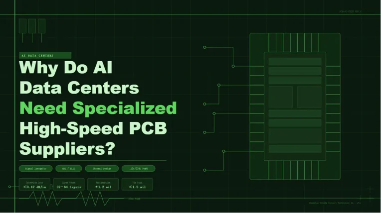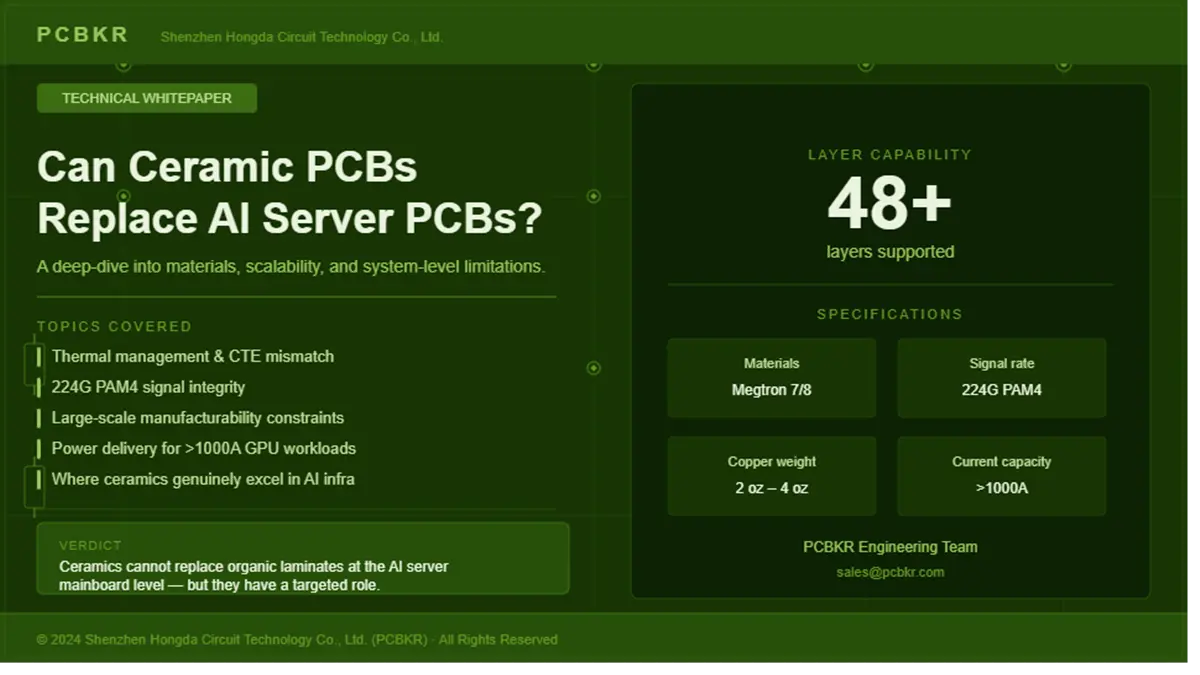
Can Ceramic PCBs Replace AI Server PCBs?
No, ceramic PCBs cannot wholesale replace AI server PCBs. While offering superior raw material thermal conductivity, severe structural limitations in multi-layer sequential lamination (>20 layers), ultra-large form factor scaling (>600 mm), multi-phase high-current power delivery (>1000 A), and brittle mechanical failure modes make them completely unviable for mainboard infrastructure.
1. What Are Ceramic PCBs and How Do They Compare to High-Speed Organic Substrates?
Ceramic PCBs utilize inorganic ceramic bases (such as Al₂O₃, AlN, or Si₃N₄) instead of traditional organic glass epoxy (FR-4) or ultra-low-loss polyphenylene ether (PPE) laminates. They provide unmatched thermal dissipation at a component level but lack the macro-scale routing density required by modern AI clusters.
Parameterized Material Performance Matrix
| Material Property / Capability | Alumina (Al₂O₃) Ceramic | Aluminum Nitride (AlN) Ceramic | Ultra-Low-Loss Organic Laminate (e.g., Megtron 8) | AI Server Motherboard Technical Requirement |
|---|---|---|---|---|
| Thermal Conductivity (W/m·K) | 24 – 30 | 170 – 230 | 0.3 – 0.5 | Critical at localized high-power ASIC hotspots. |
| Coefficient of Thermal Expansion (CTE) (ppm/°C) | 6.8 – 7.2 | 4.5 – 4.8 | 12 – 16 (X/Y-Axis) | Must manage mismatch with Silicon Dies (≈ 3 – 4 ppm/°C). |
| Maximum Feasible Layers | 2 to 8 layers | 2 to 4 layers | 20 to 40+ layers | 24 to 36+ layers minimum for dense routing. |
| Maximum Panel Form Factor | ≤ 150 × 150 mm | ≤ 200 × 200 mm | ≥ 610 × 457 mm (Standard Panel) | ≥ 600 mm system backplanes and large OAMs. |
| Dielectric Loss (Df @ 10 GHz) | ≈ 0.0004 | ≈ 0.0005 | ≈ 0.0012 | ≤ 0.0015 required to mitigate 224G PAM4 attenuation. |
| Max Single-Layer Copper Thickness | Thin Film (<10 μm), Thick Film (25 μm) | DBC Process (≥ 100 μm) | Up to 3–4 oz (105 – 140 μm) | Multi-layer 2–3 oz heavy copper lamination. |
Expert Engineering Perspective
“In high-power RF modules and localized LED architectures, ceramic substrates deliver excellent structural integrity and low dielectric loss. However, attempting to route a 224G PAM4 SerDes system on a ceramic substrate exposes fundamental manufacturing deadlocks. While raw ceramic materials boast exceptional Df values (≈ 0.0005) that surpass organic resins, they cannot support the complex lamination mechanics needed to eliminate high-speed signal bottlenecks. Organic boards easily utilize sequential High-Density Interconnect (HDI) microvias and precise back-drilling to eliminate via stubs, preserving signal integrity at 56 GHz Nyquist frequencies. In contrast, co-fired ceramics (such as LTCC or HTCC) undergo high-temperature sintering that causes non-linear shrinkage, making precision impedance matching across a large-scale motherboard virtually impossible to control.”
2. High-Speed Signal Integrity Barriers at 224G PAM4
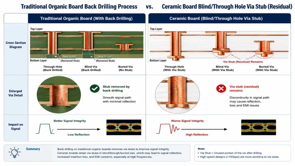
Traditional Organic Board Back Drilling vs. Ceramic Board Via Stub (Signal Integrity Comparison by PCBKR
While ceramic materials exhibit excellent low-loss dielectric properties, they fail the signal integrity criteria of next-generation AI architectures due to the physical impossibility of routing advanced 3D via structures.
- The Via Stub Dilemma: 224G PAM4 signaling demands the near-total elimination of via stubs through back-drilling or blind microvia deployment. Because multi-layer ceramic vias are formed by punching green tapes and filling them with metal paste prior to co-firing, post-fabrication mechanical back-drilling is impossible due to material brittleness, creating fatal signal reflections.
- High Impedance Mismatch in Sintering: Co-fired ceramics experience a massive 15% to 20% volumetric shrinkage during processing. This non-uniform structural shift deforms fine-line microstrip geometries, causing unpredictable impedance fluctuations that disrupt high-frequency differential pairs.
- High-Conductivity Material Incompatibility: High-Temperature Co-fired Ceramics (HTCC) require sintering temperatures up to 1600°C, forcing the use of high-resistance refractory metals like tungsten or molybdenum. These metals suffer from severe skin-effect losses at ultra-high frequencies compared to the ultra-smooth, high-conductivity HVLP copper foils laminated onto organic Megtron-class boards.
3. Geometric and Mechanical Manufacturing Bottlenecks
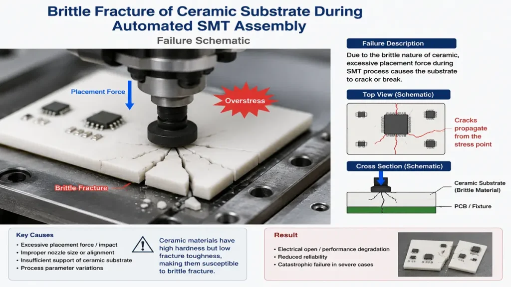
Brittle Fracture Defect of Ceramic Substrate During Automated SMT Process (PCBKR Manufacturing Advisory)
Inherent material brittleness, low fracture toughness, and exponential yield collapse at scale prevent ceramic substrates from expanding into the large-scale form factors required by data center hardware.
1. Macro-Warpage and Brittle Fracture Realities
Ceramics have excellent compressive strength but exceptionally poor tensile flexibility. As substrate dimensions cross the 300 mm threshold, internal thermal gradients during high-temperature baking induce macroscopic warpage.
Manufacturing Failure Mode: Any mechanical force applied to flatten a warped ceramic board during subsequent automated SMT pick-and-place assembly or manual rework triggers instant propagation of micro-cracks, culminating in catastrophic structural shattering.
2. Z-Axis High-Density Interconnect (HDI) Limitations
Modern AI OAMs require complex 3D routing layouts across 24 to 48 layers to split massive power distribution networks (PDN) and high-speed signal channels.
Process Bottleneck: Layering more than 8 layers of ceramic green tapes amplifies microscopic shrinkage variances in the Z-axis. This causes inner-layer via shear fractures and fluid-flow short circuits of the conductive paste during compression, dropping fabrication yields to near zero. Organic laminates bypass this entirely via precise sequential build-up and electrochemical copper plating.
4. Power Delivery Network (PDN) Deficiencies for High-Current GPUs
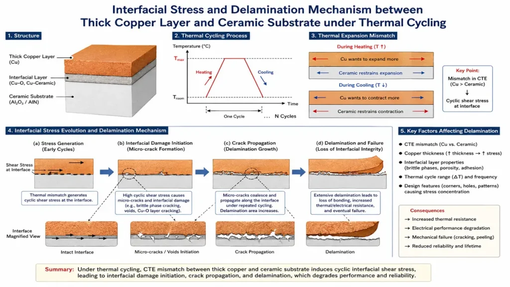
Interfacial Stress and Delamination Mechanism under Thermal Cycling (PCBKR Engineering Insights)
Ceramic PCBs cannot support the heavy-duty copper layers needed to safely channel >1000A continuous current to next-gen processors, resulting in thermal interface delamination and fatal transient voltage droops.
1. Heavy Copper Thermo-Mechanical Delamination
To deliver massive wattage at sub-1.0V core voltages, AI motherboard power planes must deploy thick copper layers (2 oz to 4 oz, or 70-140 μm) connected in parallel to lower $I^2R$ power losses.
Failure Mechanism: Bonding thick copper onto ceramic requires Direct Bonded Copper (DBC) or Active Metal Brazing (AMB) techniques. Due to the severe CTE mismatch between copper (16.5 ppm/°C) and ceramic (4.5 ppm/°C), intense thermal cycling during power spikes creates devastating shear stresses at the material interface. This rapidly induces copper peeling, blistering, or micro-cracking of the brittle ceramic base (crater failure).
+———————————————————+ | Heavy Copper Plane (Thick Foil, CTE ~ 16.5) | <– Expands Significantly +———————————————————+ |======= High Shear Stress Interface (Delamination Risk) =| <– Critical Point of Failure +———————————————————+ | Rigid Ceramic Matrix (Core Substrate, CTE ~ 4.5) | <– Rigid / Minimal Expansion +———————————————————+
2. Transient Voltage Droop and Loop Inductance Spikes
GPU Voltage Regulator Modules (VRMs) switch at high frequencies to maintain clean power rails. This requires hundreds of decoupling capacitors placed directly underneath the processor socket, connected through ultra-short via paths.
Electrical Failure Mode: Because ceramics cannot accommodate highly dense, multi-layer staggered microvia networks, the loop inductance of the PDN spikes significantly. When the GPU transitions from idle to full training loads, this elevated loop inductance triggers severe transient voltage droops, causing calculation errors, logic glitches, or hard system resets.
5. Where Ceramic PCBs Actually Excel in AI Infrastructure
Rather than replacing the mainboard, ceramic technology serves as a localized component-level supplement, deployed where thermal flux densities or optical frequencies surpass the physical limits of organic resins.
- Sub-Card Voltage Regulator Modules (VRMs): High-power DC-DC converters, discrete MOSFETs, or integrated DrMOS components are increasingly built onto independent, small-scale Aluminum Nitride (AlN) or DBC ceramic daughter cards. These micro-subcards handle heavy localized thermal loads and dump heat straight to liquid-cooling cold plates, protecting the large organic mainboard from localized thermal warping.
- 800G and 1.6T Optical Transceivers: High-bandwidth optical modules integrate power-dense laser drivers and high-frequency EML chips. Micro-scale, ultra-precise Thin-Film Ceramic Substrates are used inside these optical housings to handle tight spatial heat dissipation while maintaining pristine signal integrity into the millimeter-wave spectrum.
6. Technical Frequently Asked Questions (FAQ)
Why does the high thermal conductivity of ceramics fail to solve the macro-level cooling issues of AI servers?
Ceramic substrates (like AlN) feature exceptional thermal conductivity up to 230 W/m·K, but they cannot be scaled past 200–300 mm due to processing brittleness and warpage. Because AI server motherboards require large physical footprints (>600 mm) to interconnect multiple GPU clusters and memory networks, ceramics cannot be used for the large board area. Instead, thermal issues are resolved by using advanced liquid-cooling blocks mounted directly over organic multi-layer boards.
Why are organic laminates like Megtron 8 preferred over low-loss ceramics for 224G PAM4 routing?
Even though ceramics exhibit exceptionally low material dielectric loss, they fail at the system integration level. 224G PAM4 signaling demands strict impedance consistency and via stub elimination. Organic boards support sequential lamination, automated blind/buried laser drilling, and precision back-drilling to remove excess stub copper. Ceramic manufacturing relies on pre-sintered paste-filled vias that experience erratic shrinkages and cannot be back-drilled, resulting in uncontrollable signal reflections.
What makes the mechanical properties of ceramics a liability during automated SMT assembly?
Ceramics have very low fracture toughness. Large-area panels inevitably warp during the mandatory high-temperature co-firing stage. When automated SMT assembly lines apply mechanical clamping forces to level the board for paste printing or component placement, or during the thermal stresses of reflow soldering, the substrate cannot flex. It releases the internal stress by micro-cracking, leading to immediate structural failure.
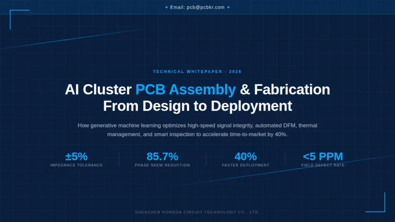
Looking for High-Layer Count, Ultra-Low-Loss AI Motherboard Solutions?
At Shenzhen Hongda Circuit Technology Co., Ltd. (PCBKR), we understand that next-generation AI infrastructure demands advanced material mastery. While ceramics solve localized component challenges, scaling up system boards requires elite organic lamination precision. We specialize in engineering and manufacturing high-density, multi-layer AI server PCBs designed to handle the most rigorous computing profiles.
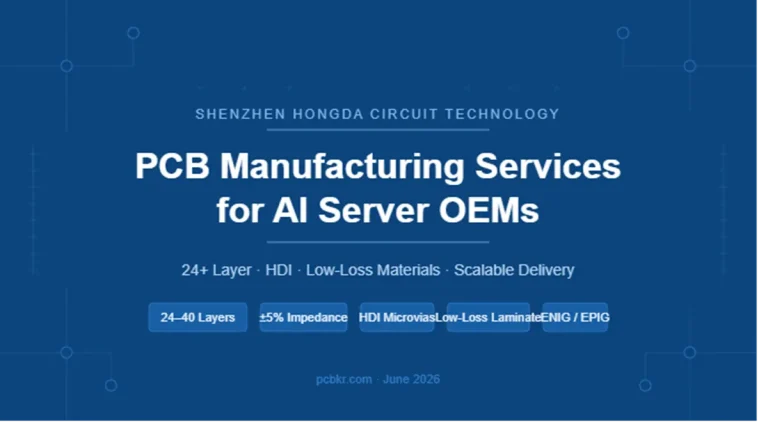
- Advanced multi-layer board capabilities up to 24–48+ layers
- Full processing compatibility with next-gen Ultra-Low-Loss materials (Megtron 7/8, Tachyon 100G)
- Precision back-drilling and depth-controlled laser routing for flawless 112G & 224G PAM4 signaling
- Heavy-copper inner layer processing (2 oz to 4 oz) tailored for extreme >1000A GPU power grids
Accelerate your hardware development with an industry-tested manufacturing partner.Contact PCBKR Engineering Team: PCB@pcbkr.com
Find Out About Us: Delivering Top-Tier Fabrication for Both AI & Conventional PCBs
Navigating the line between cutting-edge innovation and high-volume, cost-effective production shouldn’t be a compromise. At Shenzhen Hongda Circuit Technology (PCBKR), we bridge this gap by elevating the manufacturing standards for both high-performance AI hardware and traditional multi-layer PCBs.
By integrating advanced manufacturing methodologies across all production lines, we bring an elite level of precision to traditional PCB fabrication. Our standard boards benefit from enhanced interlayer alignment tolerances (down from ±75μm to within ±25μm) and tightened differential impedance control (±5%). Supported by 100% 3D X-Ray (AXI) inspection, your conventional boards achieve chip-level reliability, superb signal stability, and near-100% yield.
Your Strategic Manufacturing Partner
We proudly stand as a dual-capability partner: offering the elite technical ceiling required for next-gen AI hardware, while maintaining the exceptional flexibility, rapid turnaround, and unmatched cost-efficiency needed for mid-to-high-volume traditional board campaigns. You get zero-defect reliability without the premium overhead or bureaucracy of massive tier-1 factories.
Ready to upgrade your hardware’s reliability?
Submit your Gerber files today for an agile engineering review and a highly competitive quote.
📧 Contact our experts: sales@pcbkr.com
About Author
David Chen https://www.linkedin.com/in/pcbcoming
David Chen boasts an extensive professional background in PCBA manufacturing, PCBA testing, and PCBA optimization, with specialized expertise in high-precision PCBA fault analysis and rigorous PCBA reliability testing. The author has worked with high-layer-count server PCB fabrication, ultra-low-loss backplane stackups, and thermo-mechanical reliability optimization for AI infrastructure projects involving 112G and 224G PAM4 architectures. Skilled in complex circuit design and cutting-edge advanced PCB manufacturing processes, he delivers solutions that elevate product durability and performance across industrial applications. His technical articles focusing on PCBA manufacturing workflows and testing methodologies are widely cited by industry peers, research institutions, and technical platforms, solidifying his reputation as a recognized technical authority in the global circuit board manufacturing sector.