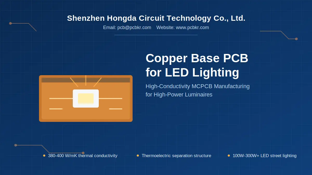
Copper Base PCB for LED Lighting: High-Conductivity MCPCB Manufacturing for High-Power Luminaires
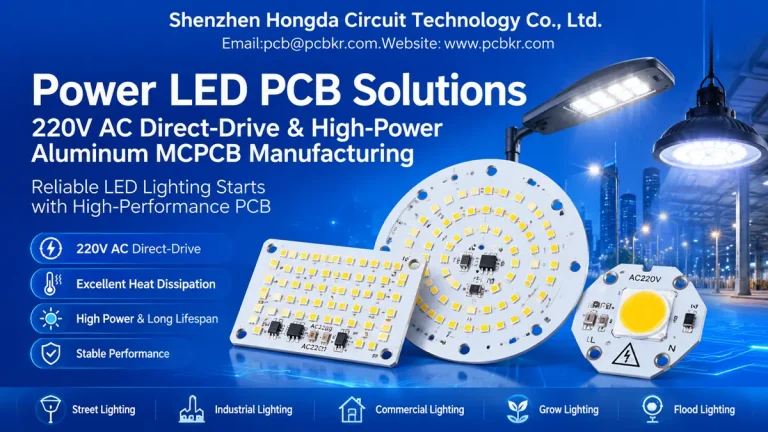
Copper Base PCB for LED Lighting delivers a targeted thermal solution to the heat challenge inherent in high-power LED lighting, an issue standard circuit boards are not engineered to resolve. As LED power ratings keep rising while lighting fixtures are designed with increasingly compact dimensions, copper base PCB—a copper core type of MCPCB (metal core PCB)—stands out as a viable solution for design engineers. It dissipates concentrated heat from LED chip sources far more efficiently than conventional FR-4 substrates and even aluminum-based metal core boards.
Shenzhen Hongda Circuit Technology Co., Ltd. manufactures premium copper base PCB for LED lighting with full adoption of 2026-era imaging, lamination and automated inspection production machinery. Our finished circuit boards reliably withstand continuous high thermal stress, making them ideal core components for street lamps, industrial high-bay lights, stage performance lighting and commercial horticultural grow light arrays supplied to lighting OEM manufacturers.
This page walks through why copper core boards outperform standard substrates in high
heat-density LED applications, what specifications matter when you write an RFQ, and how
our production floor is set up to deliver consistent quality from prototype through volume.
Why High-Power LED Chips Overwhelm Standard FR-4 and Push Designers
Toward Metal Core PCB
Point-Source Heat and the Junction Temperature Problem in LED Arrays
An LED chip is a point-source heat generator — the thermal flux is concentrated in a tiny
die area rather than spread across a board. Standard FR-4 laminate has a thermal
conductivity of roughly 0.3 W/(m·K), which is fine for logic boards but far too low to pull
heat away from a single high-current LED before junction temperature climbs. Once
junction temperature rises past the chip’s rated threshold, lumen output drops, color
temperature shifts, and the diode’s usable life shortens — the three failure modes lighting
engineers are trying hardest to avoid.
From Aluminum to Copper: The Metal Core PCB Thermal Path
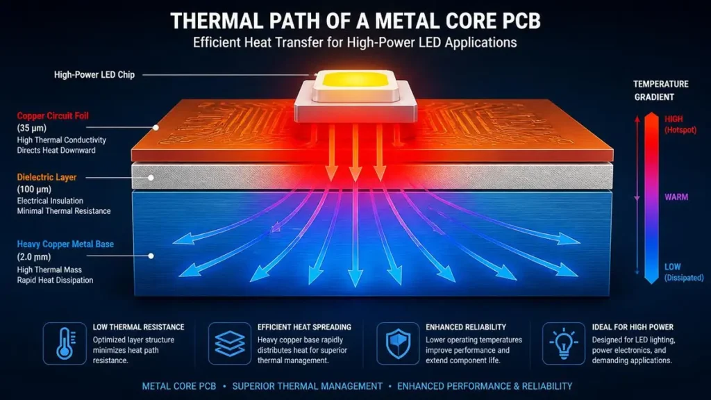
Thermal Path of Copper Base PCB for LED Lighting
A metal core PCB solves this by replacing the fiberglass core with a metal base — typically
aluminum or copper — layered under a thermally conductive dielectric and a copper circuit
foil. Heat flows from chip to copper trace, through the dielectric, into the metal base, and
out to a heatsink or housing. Aluminum PCB handles this adequately for low-to-mid
wattage fixtures. Copper base PCB extends the same principle further, because copper’s
intrinsic thermal conductivity (roughly 380–400 W/m·K) is close to double that of
aluminum (roughly 200 W/m·K), which matters once wattage, chip density, or ambient
temperature push a design past what an aluminum core can carry.
Copper Base PCB vs Aluminum MCPCB: Where Each One Actually Wins
Procurement teams often ask which metal core is “better,” but the honest answer depends
on power density and budget, not brand preference.
Copper Core PCB for High Heat-Density, High-Power Arrays
Copper base PCB is the stronger choice when:
1. Total fixture wattage sits above roughly 100W, or chip density creates a concentrated
hot zone
2. The design needs to shrink substrate thickness or overall module footprint without
giving up thermal headroom
3. Circuit traces are carrying meaningful current, since copper foil bonded to a copper
core reduces resistive losses and secondary heat buildup
4.The application is unforgiving of failure — mining lamps, stage lighting, high-bay
industrial fixtures, and outdoor high-intensity fixtures fall in this category
Aluminum PCB for Cost-Sensitive, Medium-Power Designs
Aluminum MCPCB remains the more economical option for general commercial lighting,
indoor downlights, and mid-power fixtures where thermal margins are less tight. A copper
base PCB manufacturer should be transparent about this trade-off rather than pushing
copper on every quote — matching substrate to actual thermal load is what keeps a lighting
OEM’s bill of materials sane.
2026 Manufacturing Technologies Behind Hongda’s Copper Base PCB Production
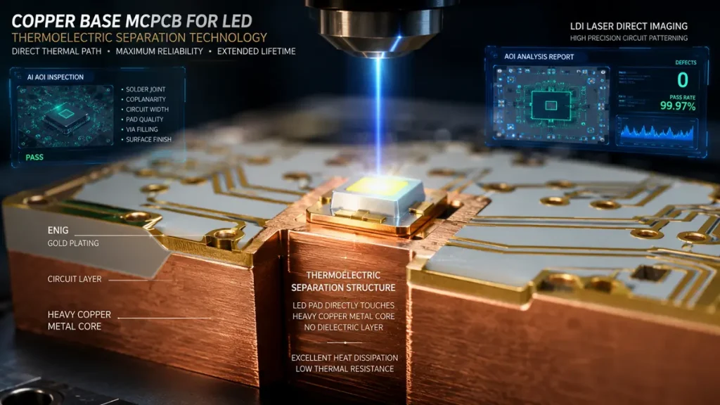
Thermoelectric Separation Structure of Copper Base PCB for LED Lighting
PCB fabrication has moved a long way past manual exposure tables and spot-check
inspection. The copper base PCB leaving our facility passes through equipment built
around three 2026-era priorities: finer circuit geometry, in-line data capture, and reduced
environmental footprint.
Laser Direct Imaging (LDI) for Fine-Line Copper Circuitry
Copper trace patterns for dense LED arrays increasingly need narrower lines and tighter
spacing than contact-exposure tooling can hold. Our laser direct imaging lines pattern
copper foil directly from CAM data, which removes phototool-related registration drift and
keeps trace width consistent across a panel — a meaningful factor when a design specifies
thermal-relief copper pours as narrow as 3–5 mm around each LED footprint.
AI-Assisted AOI and Computer Vision Inspection
Automated optical inspection stations, layered with computer-vision defect detection,
catch copper etching irregularities, dielectric voids, and pad oxidation issues that are too
small for a manual visual check. This is standard practice on high-mix production floors
now, and it is what allows a copper base PCB run to hold tight process control across
thousands of panels rather than relying on end-of-line sampling alone.
Thermoelectric Separation Structure for Multilayer Copper MCPCB
For designs that need signal routing and thermal dissipation on the same board, our
thermoelectric separation process isolates the high-thermal-conductivity zone under the
LED footprint from the surrounding circuit layers, so a copper base PCB can carry more
complex circuitry without sacrificing the direct thermal path to the metal core.
IIoT-Monitored Lamination and Closed-Loop Water Systems
Lamination presses on our floor log pressure, temperature, and cycle data in real time,
which shortens root-cause time if a lot needs rework and keeps bond-line thickness
consistent panel to panel. On the environmental side, closed-loop water recovery in the
etching and plating lines reduces fresh-water draw per panel — a requirement more
lighting OEMs are now asking suppliers to document as part of their own sustainability
reporting.
Ideal Applications for Copper Base PCB in LED Lighting
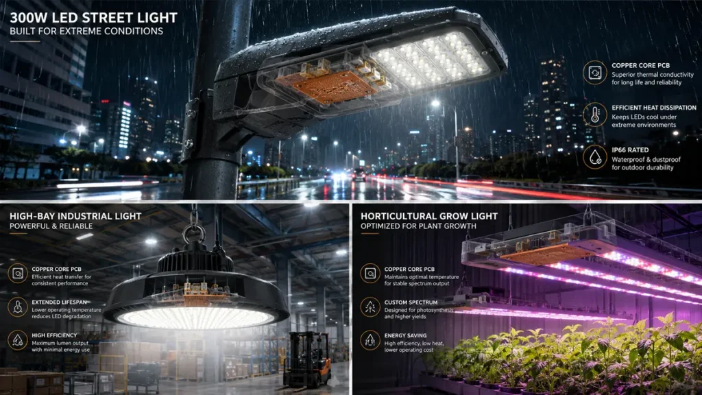
Ghosted Tech View of Copper Base PCB for LED Lighting Applications
1. High-power outdoor fixtures: 100W–300W+ LED street lights, tunnel lights, and
floodlights, where thermal failure directly shortens relamping cycles
2. Industrial and special lighting: high-bay and mining lamps, stage and studio
lighting, searchlights, and other high-intensity fixtures with dense chip layouts
3, Horticultural LED grow lights: vertical-farm and greenhouse modules that run long
duty cycles and need stable light output over years, not months
4. COB and multi-chip LED modules: integrated chip-on-board arrays where several
die sit close together and share a single thermal path to the metal core
Copper Base PCB Specification Guide: What to Put in Your RFQ
Substrate Type and Thickness
Specify high-purity or low-alloy copper base material for maximum conductivity and
mechanical strength. Common thicknesses run 1.0mm and 1.5mm for mid-power fixtures
(30–100W) and 1.5mm–2.0mm or heavier for 100W–300W+ designs paired with an external
heatsink.
Dielectric Layer Thermal Conductivity and Voltage Rating
Dielectric conductivity in the 3.0–8.0 W/(m·K) range covers most copper base PCB for LED
lighting projects; high heat-density arrays should lean toward the upper end, often using
ceramic-filled or nitride-filled epoxy systems. Voltage rating should match the driver’s
operating voltage, with 1.5kV and 2.5kV dielectric breakdown ratings being common
baselines for LED module safety compliance.
Copper Foil Weight and Thermal Trace Layout
1oz copper foil is standard; 2oz is the recommended upgrade for high-current LED circuits,
since heavier copper both carries more current and spreads heat more evenly. Thermal
pour width matters as much as thickness — a grid or bar-style copper pour under each chip,
kept at 3mm minimum (5mm on 100W+ arrays), reduces localized hot spots that a thinner
trace layout would miss.
Surface Finish and Solder Mask for Outdoor Durability
ENIG (electroless nickel immersion gold) at roughly 0.1–0.2
μ
m is the common finish for
copper base PCB in LED applications, since it resists oxidation and keeps contact resistance
— and therefore contact-point heat — low over the product’s service life. Outdoor and UV
exposed fixtures should also specify a UV- and high-temperature-resistant solder mask to
prevent insulation degradation after years in the field.
Copper vs Aluminum MCPCB: A Quick Selection Checklist
| Consideration | Copper Base PCB | Aluminum MCPCB |
|---|---|---|
| Thermal conductivity | ~380-400 W/(m·K) | ~200 W/(m·K) |
| Best fit | 100W+ high-density arrays | Mid-power, cost-sensitive designs |
| Current-carrying capacity | Higher, supports heavier copper foil | Adequate for standard LED loads |
| Weight and machining cost | Higher | Lower |
| Typical use case | Street lights, mining lamps, stage lighting, COB modules | General commercial and indoor lighting |
Procurement Checklist Before You Place a Copper Base PCB Order
Before releasing Gerber files to any copper base PCB manufacturer, it helps to have these
answered:
- LED power per chip and total fixture wattage, plus target junction temperature
- Array layout and whether the design needs thermoelectric separation for mixed
signal/thermal routing - Operating voltage and required dielectric breakdown rating
- Current per trace, to confirm copper foil weight and minimum trace width/spacing
- Environmental exposure (outdoor, high humidity, salt spray) to lock in surface finish
and solder mask spec - Panelization approach, test-point layout, and traceability requirements for volume
production
Frequently Asked Questions From Buyers Evaluating Copper Base PCB Suppliers
How do I verify a copper base PCB manufacturer’s quality control and thermal performance data before placing an order?
Ask for the supplier’s documented dielectric thermal conductivity rating, copper core thickness tolerances, and inspection method (AOI,
electrical test, cross-section verification). A manufacturer that can walk through its lamination process control and testing data on request is a stronger long-term partner than one offering only a price quote.
What is the typical minimum order quantity and lead time for a custom copper MCPCB prototype?
Lead times vary by copper thickness and panel complexity, but most
copper base PCB suppliers can turn a simple prototype in days once Gerber files, stack-up, and dielectric spec are confirmed. Ask specifically about prototype MOQ separate from production MOQ, since many suppliers set these differently.
Can the same supplier handle both prototype runs and volume production of LED boards without re-qualifying tooling?
This matters more than it looks — switching manufacturers between prototype and mass production often means re-validating thermal
performance and DFM assumptions from scratch. Confirm the supplier’s panel size range, lamination press capacity, and whether they retain your design’s DFM notes for scale-up.
What copper thickness and dielectric conductivity should I specify for a 150W LED street light board?
As a starting point, 150W-class fixtures typically pair a 1.5–2.0mm
copper base with a dielectric layer in the 5.0–8.0 W/(m·K) range and 2oz copper foil for the circuit layer, though the exact numbers depend on chip layout and heatsink design. A supplier offering thermal simulation before quoting is worth prioritizing over one that only matches a spec sheet.
Does the manufacturer provide DFM review or thermal simulation before production, or only after a problem shows up?
Pre-production DFM and thermal review catch trace width, via, and dielectric mismatches before tooling is cut, which is far cheaper than
discovering a thermal issue in a failed field sample. Ask whether DFM feedback is a standard step in the supplier’s quoting process or a paid add-on — that answer tells you a lot about how the relationship will run at volume.
Request a Quote For custom copper base PCB projects — LED street lighting, industrial
fixtures, COB modules, or horticultural grow-light boards — share your LED power and
package type, array layout, target junction temperature, and voltage/dielectric
requirements. Shenzhen Hongda Circuit Technology Co., Ltd. will return thermal guidance,
a specification recommendation, and a production quote based on your fixture’s actual
thermal load. Email:sales@david
About Author
David Chen https://www.linkedin.com/in/pcbcoming
David Chen boasts an extensive professional background in PCBA manufacturing, PCBA testing, and PCBA optimization, with specialized expertise in high-precision PCBA fault analysis and rigorous PCBA reliability testing. The author has worked with high-layer-count server PCB fabrication, ultra-low-loss backplane stackups, and thermo-mechanical reliability optimization for AI infrastructure projects involving 112G and 224G PAM4 architectures. Skilled in complex circuit design and cutting-edge advanced PCB manufacturing processes, he delivers solutions that elevate product durability and performance across industrial applications. His technical articles focusing on PCBA manufacturing workflows and testing methodologies are widely cited by industry peers, research institutions, and technical platforms, solidifying his reputation as a recognized technical authority in the global circuit board manufacturing sector.