What Is Busbar Integrated PCB Assembly and How Do You Choose the Right OEM Manufacturer?
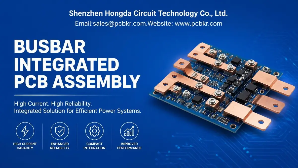
Busbar integrated PCB assembly combines a printed circuit board with copper busbars to create compact, low-resistance power paths alongside electronic control and sensing circuits. PCBKR supports PCB fabrication and SMT/THT PCBA assembly for OEM projects, with busbar integration requirements reviewed against customer drawings, electrical specifications, mechanical interfaces, and qualified processing arrangements. From prototypes to production builds, the manufacturing scope is defined around the actual project configuration.
What Is Busbar Integrated PCB Assembly?
Busbar integrated PCB assembly is an electronic manufacturing approach in which a copper conductor is combined with a PCB to carry high current through selected sections of an electronic system. The PCB supports control, sensing, protection, and communication circuits, while the busbar provides a larger conductive cross-section for power distribution.
The purpose is not simply to add a copper bar to a circuit board. The design must coordinate three functional areas:
- Power conduction: The busbar and PCB copper paths must carry the specified continuous and peak current within the permitted voltage drop and temperature limits.
- Electronic integration: The PCB must accommodate components such as current sensors, voltage sensing circuits, gate drivers, protection devices, and control interfaces.
- Mechanical and thermal integration: The busbar connection, mounting points, insulation, enclosure, and cooling conditions must work as one assembly.
This architecture is relevant when a conventional PCB copper path cannot meet the required current, temperature-rise, or packaging constraints economically.
Typical applications include battery management systems, energy storage equipment, EV power electronics, industrial motor drives, power conversion systems, high-current control units, and power distribution assemblies.
Common Busbar-Integrated PCB Architectures
The term busbar integrated PCB assembly can describe several different constructions. These should be distinguished during the RFQ process because they require different PCB designs and assembly methods.
1. PCB with an externally mounted copper busbar
A copper bar is mounted onto or connected to the PCB through bolts, soldered joints, terminals, or other specified interfaces. This arrangement can keep the PCB fabrication process relatively conventional while adding a separate high-current conductor.
2. PCB with a press-fit busbar
A busbar or dedicated conductive element is mechanically inserted into prepared plated holes or compatible connection features. The PCB hole dimensions, plating, board thickness, insertion force, and support tooling must match the selected component manufacturer’s requirements.
3. PCB with an embedded or integrated copper conductor
A shaped copper conductor is incorporated into a specialized PCB construction. This can provide a localized high-current path without increasing copper thickness across the entire board. It requires closer coordination between PCB construction, conductor geometry, insulation, and fabrication processes.
4. PCB combined with a laminated busbar
A laminated busbar is a separate power conductor assembly, often using multiple conductive layers and insulation. It may be connected to a PCB or control board as part of a larger power electronics system. Unlike a flat PCB busbar, a laminated busbar can provide a three-dimensional mechanical structure.
The appropriate architecture depends on current requirements, voltage, available space, thermal conditions, connection technology, and production volume.
Busbar PCB vs. Heavy Copper PCB vs. Laminated Busbar: Which Is Better?
These technologies address related but different engineering requirements. A busbar is not automatically a better solution than a heavy copper PCB, and a heavy copper PCB is not always the most economical option.
| Design consideration | Busbar-integrated PCB | Heavy copper PCB | Laminated busbar |
|---|---|---|---|
| Main function | Localized high-current conduction integrated with electronics | High-current routing within PCB copper layers | Power distribution between electrical assemblies |
| Current path | Separate copper conductor and PCB paths | Thick PCB copper | Formed copper or other conductive layers |
| Electronic component integration | Components can be mounted on the PCB | Direct PCB component integration | Usually requires connection to a separate PCB |
| Mechanical structure | Depends on mounting and conductor design | Primarily supported by PCB | Can provide a rigid 3D structure |
| Design flexibility | Depends on conductor and interface geometry | Depends on PCB stackup and copper design | Strong flexibility in formed 3D conductor geometry |
| Key engineering concern | Joint resistance, mounting, thermal and mechanical stress | Copper distribution, thermal rise, manufacturability | Insulation, spacing, bending, mounting and joint reliability |
When Should You Choose a Busbar-Integrated PCB?
A busbar-integrated design is worth evaluating when:
- High current is concentrated in a limited section of the circuit.
- Increasing copper weight across the entire PCB would add unnecessary cost.
- The product requires both power distribution and electronic control on one assembly.
- A separate conductor can improve the mechanical or thermal arrangement.
- The available PCB area is limited and a vertical or raised conductor path is practical.
When Is Heavy Copper PCB More Suitable?
Heavy copper PCB manufacturing may be preferable when high-current routing is distributed across several PCB areas rather than concentrated in one conductor path.
It can also be suitable when the product requires a more integrated board construction and the current, temperature-rise, and layer requirements can be met within the PCB design.
Review the heavy copper PCB manufacturing options when comparing copper weight, layer structure, trace geometry, and fabrication requirements.
When Is a Laminated Busbar More Suitable?
A laminated busbar may be a better fit when the system requires a three-dimensional conductor assembly, closely coupled power paths, defined insulation layers, or a mechanical structure that cannot be achieved with a flat PCB-based conductor.
For high-power converters, the choice may also depend on switching-loop inductance, conductor geometry, insulation, and the placement of power devices. Hybrid arrangements can combine a PCB for control and sensing with a separate busbar for the main power path.
The correct decision should be based on the complete electrical and mechanical assembly rather than the nominal current rating of an individual conductor.
Busbar Materials, Dimensions and Electrical Design
Copper is widely used for busbars because of its electrical and thermal conductivity. However, selecting a copper grade or cross-sectional area alone does not establish the current-carrying capability of the finished assembly.
The design must account for conductor length, cross-section, operating current, contact resistance, ambient temperature, cooling conditions, and the electrical connection to the rest of the system.
Copper Material and Surface Finish
The busbar drawing should identify the conductor material and applicable material standard. Depending on the application, the specification may include:
- Copper grade and conductivity requirements
- Busbar thickness, width, length, and profile
- Surface finish, such as tin, silver, or nickel plating
- Oxidation and corrosion protection requirements
- Contact-surface flatness and dimensional tolerances
- Insulation, coating, or protective covering requirements
The surface finish should be selected for the actual contact technology and operating environment. A finish suitable for a bolted connection should not automatically be assumed suitable for a press-fit or soldered interface.
Copper-to-aluminium connections also require attention to material compatibility and environmental exposure. Where dissimilar metals are used, the interface and corrosion protection should be specified as part of the assembly design.
Busbar Cross-Section and Electrical Losses
For a first-order conductor estimate, the electrical resistance of a copper busbar can be calculated using:
R = ρ × L / A
Where:
- R = Electrical resistance (Ω)
- ρ = Electrical resistivity of the conductor (Ω·m)
- L = Conductor length (m)
- A = Conductor cross-sectional area (m²)
The power loss caused by electrical resistance can be estimated using:
P = I² × R
Where:
- P = Power loss (W)
- I = Current (A)
- R = Electrical resistance (Ω)
These equations are useful for initial busbar sizing, but they do not replace thermal validation. Actual performance is affected by temperature-dependent resistance, current distribution, contact interfaces, nearby heat sources, airflow, and the enclosure.
A busbar assembly should be evaluated as a complete current path, including:
- The copper busbar itself.
- The PCB copper traces and planes.
- The busbar-to-PCB interface.
- Terminals, bolts, connectors, or press-fit contacts.
- External power connections.
A low-resistance busbar can still produce an overheated assembly if the connection interface or PCB transition becomes the limiting point.
PCB Design Parameters That Affect Busbar Integration
The PCB drawing and stackup should be reviewed together with the busbar mechanical drawing.
| PCB design parameter | Why it matters |
|---|---|
| PCB material | Affects thermal performance, insulation, mechanical stability, and operating-temperature suitability |
| Layer count and stackup | Determines power-plane arrangement, signal routing, and available copper distribution |
| Finished board thickness | Affects mechanical support and compatibility with selected terminals or press-fit components |
| Copper thickness | Influences resistance, current distribution, and fabrication capability |
| Plated through-hole dimensions | Critical for press-fit connections and terminal installation |
| Pad and annular-ring dimensions | Affect electrical connection and mechanical integrity |
| Creepage and clearance | Must meet the applicable voltage, pollution, and insulation requirements |
| Mounting-hole positions | Control busbar alignment, fastening, and mechanical support |
The final values must be established from the actual electrical design, component specifications, Gerber or ODB++ data, and customer requirements. Generic busbar dimensions should not be treated as universal PCB manufacturing rules.
How Is a Busbar Connected to a PCB?
The connection method determines the PCB interface design, assembly sequence, inspection requirements, and long-term reliability. The selected process must be compatible with both the busbar and the PCB construction.
Bolted Busbar Connections
Bolted connections are commonly considered when the busbar must be removable or connected to a larger power distribution assembly.
The design should define:
- Bolt size and material
- Hole diameter and positional tolerance
- Contact area and surface flatness
- Specified tightening torque
- Washer or locking arrangement
- Required electrical insulation and spacing
- Access for installation and maintenance
The contact surfaces must remain stable under the expected thermal and mechanical conditions. If the assembly is exposed to vibration or repeated temperature changes, the fastening design should be validated accordingly.
Soldered Busbar Connections
A soldered connection can be considered when the busbar geometry, PCB pad structure, soldering process, and thermal mass are compatible.
However, a large copper conductor can absorb substantial heat during soldering. This can make process control more difficult and increase thermal stress on nearby components and PCB materials.
The assembly specification should identify the solder alloy, joint geometry, process window, inspection criteria, and any restrictions on rework. A soldered joint should not be accepted solely because solder is visibly present; the required electrical and mechanical performance must be defined.
Press-Fit Busbar Connections
Press-fit technology can provide a solder-free electrical and mechanical connection. It is particularly relevant when a suitable busbar or power element is designed for insertion into a PCB.
This method is highly dependent on the component manufacturer’s specifications. Relevant parameters can include:
- Finished hole diameter and tolerance
- Plated-hole copper thickness
- PCB thickness and material
- Pin geometry and dimensional tolerance
- Insertion force and insertion speed
- Retention force
- Tooling alignment and PCB support
For example, Würth Elektronik’s PowerBusbar PCB documentation specifies controlled press-in conditions and requires attention to the finished hole diameter and copper plating. Its published processing information also describes supporting and aligning the PCB and busbar during insertion. These are product-specific requirements, not universal values for every press-fit busbar.
A PCB designed for a conventional soldered terminal should not be assumed suitable for a press-fit busbar without a design and process review.
Embedded Copper Busbar Construction
An embedded conductor can be appropriate when the design needs a localized high-current path within a specialized PCB structure.
The design review should address conductor thickness, position, insulation distance, resin or dielectric construction, copper-to-PCB interfaces, and the effect of the conductor on lamination and board flatness.
This is a specialized PCB construction rather than a standard PCBA operation. The manufacturing route and available process capability must be confirmed before the design is released.
How Do You Control Thermal Performance and High-Current Reliability?
Thermal performance is one of the most important factors in a busbar-integrated PCB assembly. A conductor may have sufficient theoretical cross-section but still create a local hotspot at a connection, PCB transition, or terminal.
The temperature of the finished assembly depends on electrical losses and the ability of the complete structure to dissipate heat.
Identify the Highest-Resistance Interface
The busbar, PCB path, and connection interfaces should be considered separately during design and validation.
For a connection with resistance R_c, the local power loss is:
P_c = I² × R_c
Where:
- P_c = Power loss at the connection (W)
- I = Current through the connection (A)
- R_c = Electrical resistance of the connection (Ω)
Even a small contact resistance can produce meaningful heat at high current. For this reason, the contact interface should have a defined resistance target and measurement method where required by the project.
The measurement boundary must also be specified. A four-wire measurement across the complete assembly does not necessarily identify the resistance of an individual joint unless the measurement points are properly defined.
Evaluate Temperature Rise Under Real Operating Conditions
Thermal validation should use representative operating conditions rather than relying only on conductor calculations.
Important test conditions include:
- Continuous and peak current profiles
- Ambient temperature
- Enclosure and mounting arrangement
- Natural or forced airflow
- Adjacent component heat generation
- Duty cycle and operating duration
- Maximum permitted temperature of the PCB, components, insulation, and conductor
A busbar can also act as a heat-spreading element. Würth Elektronik has published a specific PowerBusbar PF test reporting a temperature reduction of up to 53.5 K at 185 A and 40°C ambient temperature. This result applies to its stated test arrangement and should not be used as a general performance guarantee for other busbar assemblies.
Consider Mechanical Stress and Thermal Expansion
A busbar may be heavier and stiffer than the PCB to which it is connected. Its mounting and connection design must therefore account for:
- Vibration and shock
- Thermal expansion differences
- PCB bending and local stress
- Fastener preload and loosening
- Connector alignment
- Mechanical support during assembly and operation
For larger or heavier conductors, the PCB should not be expected to carry all mechanical loads unless the design has been verified for that purpose.
Validate Electrical Insulation and Separation
High-current power paths may operate at hazardous or elevated voltages. Clearance, creepage, insulation materials, conductor spacing, and protective barriers must be selected according to the application and applicable standards.
The design must also consider switching transients, short-circuit conditions, and the separation of power and low-level signal circuits. The required insulation performance depends on the working voltage, overvoltage category, pollution degree, material group, and end-product requirements.
What Is the Manufacturing and PCBA Assembly Process?
Busbar-integrated PCB assembly requires coordination between PCB fabrication, conductor preparation, mechanical integration, and electronic assembly. The exact sequence depends on the selected architecture and connection method.
A typical OEM manufacturing workflow includes the following stages.
1. Engineering Review and DFM Assessment
Before production, the manufacturing team reviews the supplied design data.
The review should cover:
- Gerber or ODB++ files
- PCB stackup and fabrication notes
- BOM and component specifications
- Busbar drawings and 3D mechanical data
- Connection method and assembly sequence
- Electrical and thermal requirements
- Mounting and enclosure constraints
- Inspection and acceptance criteria
Any conflict between the PCB layout and busbar mechanical interface should be resolved before fabrication.
2. PCB Fabrication
The PCB is manufactured according to the approved fabrication data and stackup.
Relevant controls may include:
- Base material and laminate selection
- Layer registration
- Copper thickness
- Finished hole size and plating
- Board thickness and dimensional tolerance
- Surface finish
- Electrical continuity and insulation requirements
For press-fit designs, the PCB must follow the selected press-fit component’s hole and plating specifications. These requirements should be confirmed before the PCB enters production.
For projects requiring specialized copper structures or high-current routing, the fabrication design may also need review against high-current PCB manufacturing requirements.
3. Busbar and Interface Preparation
The busbar is prepared according to the approved mechanical drawing and material specification.
Depending on the project, this may involve cutting, drilling, forming, surface treatment, insulation, or other conductor-processing steps. These operations require suitable process resources and inspection controls.
The scope of busbar fabrication and sourcing should be confirmed during the RFQ. It should not be assumed to be included in PCB fabrication or standard SMT assembly.
4. PCB and Busbar Integration
The PCB and busbar are assembled using the approved connection method.
This may involve bolting, soldering, press-fit insertion, or a specialized embedded construction. Each method requires its own tooling, assembly instructions, and inspection criteria.
The assembly plan should define:
- Component and conductor positioning
- Required support fixtures
- Fastening or insertion parameters
- Joint inspection method
- Protection of nearby components
- Rework restrictions
- Traceability requirements
5. SMT and THT Assembly
After the applicable PCB and busbar integration steps are confirmed, electronic components are assembled according to the project sequence.
Depending on the product, this may include:
- SMT component placement and reflow soldering
- Through-hole component insertion and soldering
- Power components and connectors
- Current and voltage sensing circuits
- Control and protection components
- Inspection and electrical testing
The order of busbar integration and PCBA assembly must be defined according to the conductor design, component clearance, thermal exposure, and accessibility of the connection points. There is no single assembly sequence suitable for every design.
6. Final Inspection and Project Validation
The completed assembly is inspected against the approved drawings and project acceptance criteria.
Depending on the project, the inspection plan may include visual inspection, AOI, X-ray, electrical continuity, insulation testing, contact-resistance measurement, torque verification, and thermal testing.
Not every inspection method is required for every busbar assembly. The test scope should be agreed before production and recorded in the project quality plan.
What Inspection and Testing Are Required for Busbar Integrated PCBA?
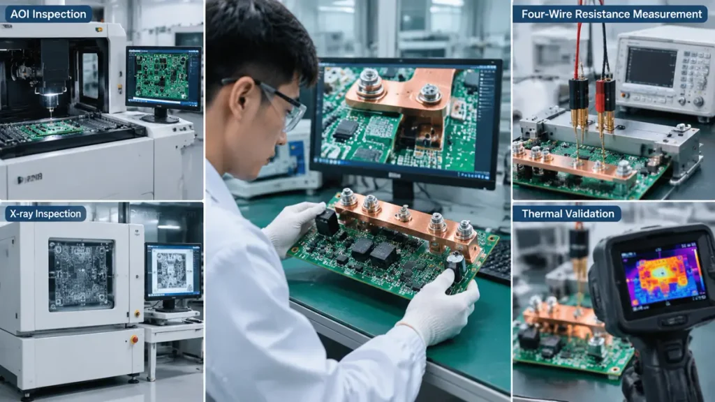
Busbar integrated PCB assembly manufacturing process with copper busbar integration and SMT PCBA
A reliable busbar-integrated PCBA needs more than a standard PCB electrical test. The acceptance plan should cover the electrical and mechanical interfaces that carry the operating current.
| Inspection or test | Main purpose | Project-specific consideration |
|---|---|---|
| Visual inspection | Check conductor position, solder joints, surface condition, and assembly workmanship | Define acceptable joint and surface conditions |
| AOI | Inspect applicable SMT solder joints and component placement | AOI does not verify the internal integrity of every busbar interface |
| X-ray inspection | Examine hidden solder joints or selected internal connection features | Use where the construction and defect type justify it |
| Electrical continuity | Confirm the specified conductive paths | Define test points and acceptable limits |
| Four-wire resistance measurement | Measure low-resistance paths or joints | Specify measurement points, current, temperature, and limits |
| Insulation resistance or dielectric test | Verify insulation performance where required | Test voltage and acceptance criteria must match the product specification |
| Torque verification | Check bolted joint installation | Define torque values and recording requirements |
| Thermal test | Evaluate temperature rise under defined current and cooling conditions | Specify operating current, ambient temperature, duration, and sensor locations |
| Mechanical or vibration test | Assess the stability of the conductor and PCB connection | Apply the relevant product qualification requirements |
A particularly important issue is the difference between testing the bare PCB and validating the assembled power path. A board can pass continuity testing while a busbar joint still has excessive resistance or insufficient mechanical retention.
For projects with high current or strict temperature limits, the acceptance plan should identify the exact connection interfaces that require additional measurement.
Which Applications Use Busbar Integrated PCB Assemblies?
Busbar-integrated PCBs are relevant to products that combine high-current distribution with electronic control or monitoring.
Battery Management and Energy Storage
Battery systems may require high-current connections alongside voltage monitoring, current sensing, protection, and communication circuits.
A busbar can provide a dedicated power path, while the PCB supports the electronic functions. The design must account for cell connections, insulation, temperature monitoring, fault conditions, and mechanical packaging.
EV Power Electronics and Charging Equipment
Power conversion and charging systems may use busbars to connect power devices, capacitors, terminals, and PCB-based control circuits.
The integration design should consider current distribution, switching behavior, insulation, thermal management, and vibration.
Industrial Motor Drives and Power Supplies
Industrial drives and power conversion equipment often combine power switching circuits with control, feedback, and protection functions.
A busbar can simplify selected high-current connections, while the PCB provides the electronic interface. The complete design must be evaluated for switching current, heat generation, electrical spacing, and mechanical mounting.
For related PCB construction requirements, review power supply PCB manufacturing.
Industrial Power Distribution and Control Equipment
Some industrial systems need compact assemblies that combine power distribution, sensing, and control. A busbar-integrated PCB can reduce the number of separate interconnections when the electrical and mechanical design supports this architecture.
The final configuration depends on rated current, voltage, enclosure, installation conditions, and applicable product standards.
How Do You Select a Busbar Integrated PCB Assembly Manufacturer?
A supplier should be evaluated on its ability to manage the complete PCB and PCBA manufacturing scope, not only on whether it can produce a copper conductor or fabricate a circuit board.
For overseas OEM buyers, the following points are particularly important.
1. Confirm the Actual Manufacturing Scope
Ask the supplier to identify which operations are performed directly and which are coordinated through qualified external resources.
The quotation should distinguish:
- PCB fabrication
- Busbar material sourcing
- Busbar cutting, drilling, or forming
- Surface treatment and insulation
- Busbar-to-PCB integration
- SMT and THT assembly
- Final electrical and mechanical testing
This prevents misunderstandings about whether the quoted price covers a bare PCB, a partially assembled board, or a complete busbar-integrated PCBA.
2. Review Experience with the Required Connection Method
The supplier should understand the selected interface and its manufacturing requirements.
For example, a press-fit design requires compatible finished-hole dimensions, copper plating, insertion tooling, and force control. A bolted connection requires defined contact geometry and fastening requirements. A soldered connection requires a suitable thermal process and joint inspection criteria.
Ask for relevant process documentation or project evidence rather than relying on a general statement that the supplier supports high-current assemblies.
3. Check Electrical and Thermal Validation Capability
The supplier should be able to agree on the required electrical measurements and inspection boundaries.
For low-resistance power connections, four-wire measurement may be appropriate. For high-current applications, thermal validation should use a defined test setup and representative operating conditions.
The acceptance criteria should be agreed before production rather than added after a sample has been assembled.
4. Evaluate Engineering Communication and DFM Support
Busbar integration involves PCB design, conductor geometry, mechanical interfaces, and assembly sequence. A supplier should be able to identify missing drawings, conflicting dimensions, unsuitable hole specifications, and unclear inspection requirements before production.
Clear engineering communication is particularly important when the OEM customer supplies the design but expects the manufacturer to coordinate the manufacturing process.
5. Confirm Prototype and Production Arrangements
The prototype process should be representative of the intended production method wherever practical.
Before placing a production order, confirm:
- Prototype quantity and lead time
- Production quantity and capacity
- Approved material and component sources
- Process and inspection records
- Revision control
- Rework and change-control requirements
- Packaging and shipment requirements
A low-cost prototype is not necessarily a reliable indicator of production cost if the final design requires additional fixtures, special processing, or qualification tests.
What Information Should You Provide for a Busbar Integrated PCB Assembly Quote?
A complete RFQ package helps the manufacturer evaluate the technical scope and return a more accurate quotation.
| RFQ information | Recommended files or details |
|---|---|
| PCB fabrication data | Gerber or ODB++ files |
| PCB construction | Layer count, stackup, material, finished thickness, copper weight |
| Component information | BOM with manufacturer part numbers and approved alternatives |
| Assembly data | Pick-and-place file, assembly drawings, polarity and orientation details |
| Busbar design | 2D manufacturing drawing and 3D STEP file where available |
| Electrical requirements | Working voltage, continuous current, peak current, duty cycle, and allowable voltage drop |
| Thermal requirements | Ambient temperature, maximum temperature rise, cooling method, and test conditions |
| Mechanical requirements | Mounting points, dimensions, clearances, enclosure data, and vibration conditions |
| Connection details | Bolted, soldered, press-fit, embedded, or other specified interface |
| Quality requirements | Inspection plan, electrical tests, mechanical tests, and acceptance criteria |
| Commercial requirements | Prototype quantity, annual demand, target lead time, and delivery destination |
If some specifications are not yet finalized, identify them as open engineering items. A manufacturer can then distinguish confirmed requirements from assumptions that need review.
The RFQ should also state whether the customer expects the supplier to provide the busbar, assemble customer-supplied conductors, or coordinate the complete manufacturing package.
Busbar Integrated PCB Assembly OEM Manufacturing by PCBKR
PCBKR provides PCB fabrication and PCBA manufacturing services for overseas OEM customers developing power electronics, industrial control, and other electronic products.
For busbar-integrated PCB projects, the manufacturing scope can be reviewed around the customer’s PCB data, BOM, busbar drawings, connection requirements, and inspection specifications.
PCBKR’s project scope can include:
- PCB fabrication based on approved Gerber or ODB++ data
- Multilayer PCB manufacturing according to the specified stackup
- SMT and THT component assembly
- Coordination of PCB and busbar interface requirements
- Review of assembly sequence and mechanical clearance
- AOI, X-ray, and electrical inspection where applicable
- Project-specific testing according to agreed acceptance criteria
Busbar sourcing, conductor fabrication, special forming, plating, insulation, and dedicated press-fit operations are subject to project review and confirmation of qualified processing resources. These services should be specified in the quotation rather than assumed to be part of standard PCB fabrication or PCBA assembly.
The final manufacturing and testing scope depends on the approved drawings, BOM, electrical requirements, selected connection method, and customer quality specifications.
Request a Busbar Integrated PCB Assembly Quotation
If you are sourcing a manufacturer for a busbar-integrated PCB or PCBA project, send PCBKR the available design files and project requirements for an initial review.
For a technical quotation, please provide:
- Gerber or ODB++ files
- BOM and assembly files
- Busbar 2D drawing or 3D model
- Rated voltage and current requirements
- Connection method and mechanical constraints
- Prototype and production quantities
- Required inspection and testing scope
Contact PCBKR
Email: sales@pcbkr.com
Website: https://www.pcbkr.com/
PCBKR can review the available project information, clarify the manufacturing boundary, and provide a quotation based on the confirmed PCB fabrication and PCBA assembly requirements.
FAQ: What Should Buyers Ask a Busbar PCB Assembly Supplier?
Can one manufacturer provide both PCB fabrication and busbar-integrated PCBA assembly?
Yes, provided the supplier can manage the required PCB fabrication and electronic assembly processes and has a confirmed arrangement for the busbar-related operations. Buyers should ask for a clear scope covering PCB production, conductor sourcing or preparation, mechanical integration, SMT/THT assembly, and final inspection. PCBKR supports PCB fabrication and PCBA assembly; busbar-specific processing is reviewed and confirmed according to each project’s requirements.
What files are required to get a quotation for busbar-integrated PCB assembly?
A typical RFQ package includes Gerber or ODB++ files, PCB stackup, BOM, pick-and-place data, assembly drawings, and a busbar 2D drawing or 3D STEP model. Buyers should also provide rated voltage, continuous and peak current, thermal limits, connection method, required tests, and estimated order quantities. If some information is unavailable, identify the open items so the supplier can assess what is needed before quotation.
How do I verify whether a busbar PCB assembly supplier can meet my current and temperature requirements?
Ask the supplier to review the complete current path, including the busbar, PCB copper, terminals, and connection interfaces. Request defined resistance measurement points, test current, ambient conditions, temperature-rise limits, and the proposed thermal validation method. A conductor’s theoretical current capacity alone is not sufficient evidence that the assembled product will meet its operating requirements.
Is a busbar-integrated PCB more cost-effective than a heavy copper PCB?
It depends on where the high current flows and how the product is constructed. A busbar can be economical when high current is concentrated in a limited section, avoiding the need for heavy copper across the entire PCB. Heavy copper PCB may be more suitable when high-current routing is distributed across multiple board areas. A fair cost comparison should include PCB fabrication, busbar material and processing, assembly, tooling, inspection, and qualification costs.
Can PCBKR manufacture prototypes and mass-produce busbar-integrated PCB assemblies?
PCBKR supports PCB fabrication and PCBA projects from prototype and small-batch requirements through production orders, subject to project review and confirmed manufacturing arrangements. For busbar-integrated assemblies, the conductor supply, connection process, tooling, inspection, and testing scope must be confirmed before production. Buyers can submit the design files, busbar drawings, BOM, and quantity forecast to sales@pcbkr.com for an initial review.
About Author
David Chen LinkedIn Profile
David Chen is a Senior RF/PCB Process Engineer at Shenzhen Hongda Circuit Technology Co., Ltd., with over 12 years of experience in high-frequency PCB fabrication, impedance-controlled stack-up design, and Rogers/PTFE laminate processing. He also boasts an extensive professional background in PCBA manufacturing, PCBA testing, and PCBA optimization, with specialized expertise in high-precision PCBA fault analysis and rigorous PCBA reliability testing. The author has worked with high-layer-count server PCB fabrication, ultra-low-loss backplane stackups, and thermo-mechanical reliability optimization for AI infrastructure projects involving 112G and 224G PAM4 architectures. Skilled in complex circuit design and cutting-edge advanced PCB manufacturing processes, he delivers solutions that elevate product durability and performance across industrial applications. His technical articles focusing on PCBA manufacturing workflows and testing methodologies are widely cited by industry peers and technical platforms, and have gained attention and recognition from industry colleagues.