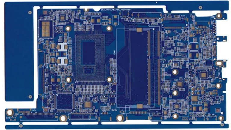
High Current PCB: Design, Copper Thickness, Thermal Management & Manufacturing
Abstract
A High Current PCB must do more than carry electrical current. It must control conductor temperature rise, voltage drop, copper resistance, via resistance, current density, thermal dissipation, and long-term reliability across the complete current path. The most common manufacturing mistake is to treat high-current performance as a trace-width problem alone. In practice, the trace, pad, via, copper plane, layer transition, connector, and terminal can all become current bottlenecks.
This guide explains how to design, manufacture, inspect, and procure High Current PCBs using IPC-based engineering principles. It covers copper thickness, trace width, heavy copper, via arrays, voltage drop, thermal management, multilayer power distribution, manufacturing tolerances, testing, RFQ requirements, and manufacturer selection. It also explains how advanced PCB manufacturing technologies—including precision LDI, controlled plating, laser drilling, multilayer lamination, AOI, X-ray inspection, and electrical testing—affect the manufacturability and reliability of high-current circuit boards.
For OEMs and procurement teams, the objective is not simply to find a PCB supplier that can produce thick copper. The objective is to establish a repeatable, measurable, and manufacturable current path from the source to the load.
What Is a High Current PCB?
A High Current PCB is a printed circuit board designed to carry relatively high electrical current while maintaining acceptable temperature rise, voltage drop, electrical resistance, mechanical integrity, and long-term reliability.
The important engineering point is that high current capability is a system property, not simply a trace property.
A typical current path may look like:
Power source → connector → PCB trace → pad → via array → copper plane → power device → return path → connector
Every section of this path contributes resistance and heat.
IPC-2152 defines current-carrying capacity in relation to conductor size and acceptable conductor temperature rise. Its scope specifically addresses the relationship between current, conductor size, and temperature in printed-board design.
Therefore, a High Current PCB design should evaluate at least:
- Continuous current
- Peak current
- Duty cycle
- Copper thickness
- Conductor width
- Conductor length
- Internal versus external layer
- Allowable temperature rise
- Ambient temperature
- Via configuration
- Copper plane area
- Connector resistance
- Voltage drop
- Thermal dissipation
A wider trace may increase current capacity, but it does not automatically solve a poorly designed via transition or undersized connector.
How Much Current Can a High Current PCB Carry?
There is no universal current value for a High Current PCB.
A PCB carrying 10 A may require a completely different structure from a board carrying 50 A or 100 A because current capacity depends on conductor geometry, copper thickness, temperature rise, thermal environment, and the complete current path.
For preliminary design, engineers commonly consider IPC-2152 together with the actual board construction and thermal conditions. IPC-2152 is intended to guide the selection of finished-board conductor dimensions according to required current capacity and acceptable temperature rise.
High Current PCB Current-Capacity Design Inputs
| Parameter | Why It Matters |
|---|---|
| Continuous current | Determines sustained thermal loading |
| Peak current | Determines short-duration electrical and thermal stress |
| Copper thickness | Determines conductor cross-sectional area |
| Trace width | Determines conductor cross-sectional area |
| Trace length | Directly affects resistance and voltage drop |
| Layer position | Changes heat dissipation |
| Temperature rise | Defines thermal operating margin |
| Ambient temperature | Determines starting thermal condition |
| Via structure | Controls current transfer between layers |
| Copper plane | Spreads current and heat |
| Connector | May become the current bottleneck |
| Duty cycle | Determines average thermal load |
This is why a reliable High Current PCB design should never be specified only as:
“50 A PCB.”
A better engineering specification is:
“50 A continuous current, 70 A peak current, maximum 20°C conductor temperature rise, defined ambient temperature, specified copper thickness, defined current path and verified voltage drop.”
How Do You Calculate High Current PCB Trace Width?
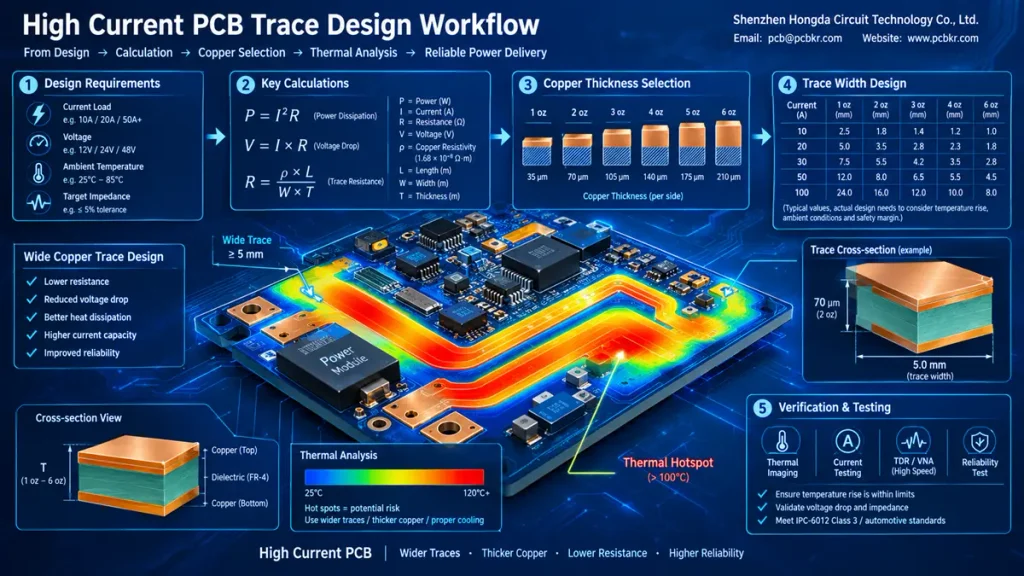
High Current PCB Trace Width & Thermal Design Calculation Workflow
The starting point for High Current PCB trace width is not a fixed ampacity chart. The engineering workflow should begin with the electrical and thermal requirements.
High Current PCB Trace Width Calculation Workflow
- Define continuous current.
- Define peak or pulse current.
- Define allowable temperature rise.
- Define ambient temperature.
- Select copper thickness.
- Determine initial conductor width.
- Calculate conductor resistance.
- Calculate voltage drop.
- Calculate I²R power dissipation.
- Review thermal behavior.
- Check PCB manufacturing capability.
- Verify the complete current path.
The relationship between conductor size and current capacity is why IPC-2152 remains an important reference for PCB current-carrying design.
Why Trace Width Alone Is Not Enough
Consider two designs with the same 10 mm-wide copper trace.
Design A
- 2 oz copper
- Short current path
- Large copper plane
- Multiple parallel vias
- Good thermal dissipation
Design B
- 1 oz copper
- Long current path
- Narrow pad transition
- Single via
- High ambient temperature
The two designs may have very different voltage drop and temperature behavior.
For procurement, this distinction is important because a supplier should evaluate the finished construction, not simply repeat a generic trace-width calculator result.
Does Copper Thickness Increase High Current PCB Capacity?
Yes. Increasing copper thickness increases conductor cross-sectional area and can reduce conductor resistance for a given width.
Typical nominal copper references include:
| Copper Weight | Approximate Copper Thickness |
|---|---|
| 1 oz | 35 µm |
| 2 oz | 70 µm |
| 3 oz | 105 µm |
| 4 oz | 140 µm |
| 6 oz | 210 µm |
| 8 oz | 280 µm |
| 10 oz | 350 µm |
These values are nominal engineering references; the actual finished copper specification must be defined by the fabrication drawing and manufacturing process.
PCBWay, for example, describes heavy copper PCB construction as commonly using 3 oz or greater copper and identifies thicker copper as one approach for higher-current designs.
High Current PCB Copper Thickness Is Not the Same as Starting Foil
Procurement teams should distinguish:
- Starting copper foil
- Finished copper
- Plated copper
- Outer-layer copper
- Inner-layer copper
- Local heavy-copper structures
For a high-current design, the relevant engineering question is not simply:
“Is this a 3 oz PCB?”
It is:
“What finished conductor thickness will exist at the critical current-carrying locations?”
This distinction becomes particularly important when copper thickness, etching, plating, line width, impedance, and registration must all be controlled simultaneously.
Is a High Current PCB the Same as a Heavy Copper PCB?
No.
High Current PCB describes the electrical function and application requirement.
Heavy Copper PCB describes a manufacturing construction involving substantially thicker copper.
A High Current PCB can use:
- Wider standard copper
- Heavy copper
- Copper planes
- Parallel PCB layers
- Multiple vias
- Copper busbars
- Hybrid power structures
Likewise, a heavy copper board is not automatically a correctly engineered High Current PCB.
A board can have thick copper and still suffer from:
- Via bottlenecks
- Poor thermal design
- Excessive voltage drop
- Connector limitations
- Current crowding
- Poor layer transitions
The design target should therefore be:
Optimize the complete current path, rather than maximizing copper thickness everywhere.
How Should High Current PCB Vias Be Designed?
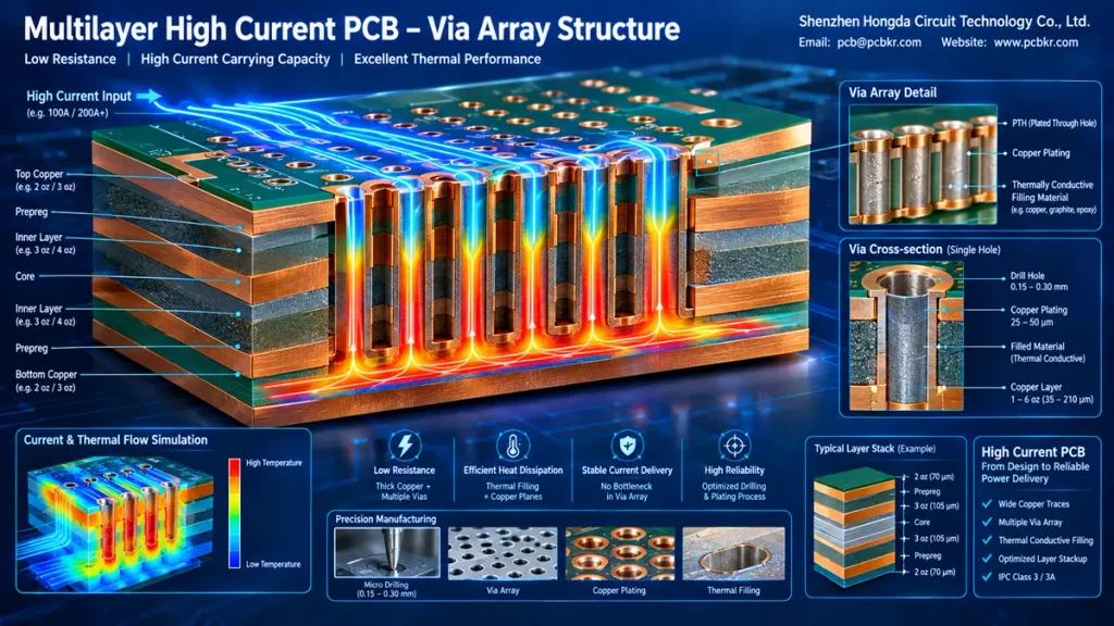
Multilayer High Current PCB Via Array Structure & Thermal Cross-Section
The High Current PCB via is one of the most frequently underestimated elements of a high-current design.
A wide copper trace may carry substantial current, but if that trace connects to another layer through a single small via, the via can become the electrical and thermal bottleneck.
High Current PCB Via Current Path
The practical path may be:
Trace → Pad → Via barrel → Internal plane → Via → Trace
Each transition introduces resistance.
For this reason, high-current designs frequently use:
- Parallel vias
- Via arrays
- Larger finished holes
- Larger copper pads
- Multiple layer transitions
- Dedicated power vias
- Large copper landing areas
PCBWay’s current high-current design guidance similarly recommends distributing current through via arrays rather than relying on a single via.
However, a fixed rule such as “one via equals X amps” should not be treated as a universal engineering specification. Via current capability depends on hole size, plating thickness, barrel length, temperature rise, surrounding copper, and current distribution.
How Many Vias Do You Need for a High Current PCB?
There is no universal number.
The correct number depends on:
- Required current
- Via finished hole
- Via barrel length
- Copper plating
- Allowable temperature rise
- Layer structure
- Current distribution
- Available pad area
- Manufacturing tolerance
A practical design sequence is:
Required current → required conductive cross-section → parallel via count → current distribution → thermal verification
High Current PCB Via Array Example
Instead of:
50 A → one via
an engineering approach should be:
50 A → determine required current-transfer area → distribute through multiple parallel vias → verify current density and temperature rise.
The objective is to prevent a localized bottleneck.
How Does Temperature Rise Affect High Current PCB Design?
Temperature rise is one of the most important parameters in a High Current PCB.
Electrical power dissipated by a resistive conductor can be represented by:
P = I²R
This relationship is particularly important at high current because power loss increases with the square of current.
If current increases significantly while resistance remains constant, heat generation can increase rapidly.
High Current PCB Thermal Design Must Consider
- Copper thickness
- Trace width
- Trace length
- Copper planes
- Ambient temperature
- Airflow
- Enclosure
- Thermal vias
- Heat sinks
- Component temperature
- Duty cycle
A 20 A continuous design in a 25°C laboratory environment should not automatically be considered equivalent to a 20 A design inside a sealed 60°C industrial enclosure.
Continuous Current vs Peak Current
A High Current PCB specification should distinguish:
Continuous current from Peak current and Pulse current.
A short-duration current pulse may produce a different thermal response from continuous operation.
How Do You Reduce Voltage Drop in a High Current PCB?
High-current design is not only a thermal problem.
It is also a voltage-drop problem.
The basic relationship is:
V = I × R
Therefore, voltage drop can be reduced by reducing current-path resistance.
High Current PCB Voltage-Drop Reduction Methods
- Increase copper cross-sectional area
- Increase trace width
- Increase copper thickness
- Reduce current-path length
- Use larger copper planes
- Use parallel PCB layers
- Increase the number of parallel vias
- Reduce connector/contact resistance
- Improve terminal construction
This becomes especially important in:
- Battery systems
- DC-DC converters
- Motor drives
- Server power distribution
- AI power systems
- EV electronics
- Energy-storage systems
For a procurement engineer, voltage-drop requirements should therefore be included in the RFQ rather than left as an assumption.
How Do You Design a High Current PCB Power Path?
A High Current PCB should be designed as a complete power-distribution structure.
High Current PCB Power Path
Source → Connector → PCB copper → Power device → Plane → Via → Load → Return path
The engineering review should identify the narrowest or highest-resistance section.
High Current PCB Bottleneck Analysis
| Potential Bottleneck | Typical Problem |
|---|---|
| Trace | Excessive resistance |
| Pad | Reduced conductive area |
| Via | Insufficient current-transfer area |
| Layer transition | Current crowding |
| Plane | Insufficient copper distribution |
| Connector | Contact resistance |
| Terminal | Local heating |
| Return path | Excessive voltage drop |
This is one of the most important practical lessons in high-current PCB engineering:
The maximum current capacity of the complete path can be limited by its smallest electrical bottleneck.
What PCB Materials Are Suitable for High Current Applications?
The correct PCB material depends on the complete electrical and thermal environment.
Standard FR-4
Suitable for many conventional power-electronics applications when the thermal design remains within the laminate and assembly requirements.
High-Tg FR-4
Can be considered when higher operating or processing temperatures require greater thermal stability.
Metal-Core PCB
Useful where direct thermal management is a primary design objective.
Aluminum Base PCB
Frequently used for LED and thermally intensive applications where heat must be transferred efficiently from components into the metal substrate.
Heavy Copper PCB
Useful where the electrical current path requires greater copper cross-sectional area.
The material should therefore be selected based on:
Current + temperature + dielectric requirements + mechanical requirements + thermal architecture.
When Should You Use Heavy Copper, Parallel Layers or Copper Busbars?
There is no single solution for every High Current PCB.
| Requirement | Potential Solution |
|---|---|
| Moderate current | Wider copper traces |
| Higher current | Thicker copper |
| Distributed current | Copper planes |
| Limited routing width | Heavy copper |
| High current across layers | Parallel vias |
| Very high current | Parallel PCB layers |
| Extreme current density | Copper busbar / hybrid structure |
| High thermal load | Metal-core / thermal architecture |
The correct choice depends on current, space, thermal constraints, cost, manufacturability, and mechanical integration.
What Are the Main High Current PCB Manufacturing Challenges?
The biggest High Current PCB manufacturing pain point is not simply producing thick copper.
The difficult part is maintaining consistent conductor geometry and electrical performance across the entire manufacturing process.
High Current PCB Manufacturing Pain Point #1: Copper Thickness vs Etching
Thicker copper requires more careful control of:
- Etching compensation
- Line width
- Sidewall geometry
- Copper distribution
- Plating
- Feature spacing
As copper becomes thicker, manufacturing becomes increasingly sensitive to process variation.
High Current PCB Manufacturing Pain Point #2: Copper Thickness vs Fine-Line Requirements
High-current PCB designs increasingly combine:
- Heavy copper power paths
- Fine-pitch BGA
- High-density signal routing
- Controlled impedance
- Small vias
These requirements can compete with one another.
A design may require thick copper for power and fine geometries for high-speed or high-density signals.
The manufacturing challenge is therefore:
How can the factory maintain both current-carrying copper and precision signal geometry on the same board?
This is where advanced imaging, plating, lamination, and registration technologies become important.
High Current PCB Manufacturing Pain Point #3: Via Reliability
A high-current via is not merely a hole.
Its performance depends on:
- Hole geometry
- Copper barrel
- Plating
- Registration
- Layer connection
- Thermal cycling
- Mechanical stress
IPC-6012F specifically expanded requirements in areas including internal plated layers, hole registration, microsection evaluation, and via-related reliability considerations.
High Current PCB Manufacturing Pain Point #4: Thermal Expansion
Large copper structures and multilayer constructions can create different thermal-mechanical behavior during:
- Lamination
- Drilling
- Plating
- Soldering
- Reflow
- Thermal cycling
This is why high-current PCB manufacturing should be engineered at the stackup and process level, not only at the routing level.
How Do Advanced PCB Manufacturing Technologies Affect High Current PCB Production?
At Shenzhen Hongda Circuit Technology Co., Ltd., advanced manufacturing technologies are relevant to High Current PCB production because high-current boards increasingly combine power structures with high-density and high-speed circuitry.
Our published manufacturing capability includes high copper constructions, with the capability page listing outer-layer finished copper up to 8 oz and a 2026 upgrade to 10 oz / approximately 350 µm for power PCB applications. These figures should be treated as project-dependent manufacturing capability rather than an automatic specification for every board.
SCREEN Ledia LDI for Precision Imaging
Laser Direct Imaging helps control circuit imaging without relying on conventional phototool alignment.
For High Current PCB manufacturing, precision imaging can contribute to:
- Trace-width consistency
- Registration
- Pad geometry
- Fine-line/high-current hybrid designs
- Repeatability between layers
PCBKR’s published equipment information identifies SCREEN Ledia LDI within its current manufacturing configuration.
Mitsubishi UV/CO₂ Laser Drilling
Laser drilling is particularly relevant when a High Current PCB also contains HDI or high-density signal structures.
PCBKR’s published capability information identifies Mitsubishi UV/CO₂ hybrid laser drilling for microvia structures, including 75 µm-class microvias in its equipment configuration.
This does not mean that every high-current board requires microvias. Instead, the technology allows power and high-density signal requirements to coexist within a more complex multilayer architecture.
Controlled Lamination
High-current multilayer boards require stable dielectric and copper registration.
PCBKR’s published equipment information includes LAUFFER vacuum lamination equipment with pressure profiling and vacuum control for advanced multilayer structures.
Advanced Plating and Copper Distribution
For high-current applications, copper plating is particularly important around:
- Through-hole vias
- Power vias
- Heavy copper structures
- Internal connections
- Layer transitions
A thick copper design is only useful if the manufacturing process can maintain the required finished structure consistently.
How Does PCBKR’s Advanced Equipment Support High Current PCB Manufacturing?
Shenzhen Hongda Circuit Technology Co., Ltd. integrates precision PCB fabrication and inspection technologies within its Shenzhen manufacturing operation.
Our published technology portfolio includes:
- LDI imaging
- HDI laser drilling
- mSAP processing
- Multilayer sequential lamination
- 3D AOI
- X-ray inspection
- Flying-probe testing
- TDR/VNA testing
- Advanced PCB materials
- High-density multilayer fabrication
These technologies are not all required for every High Current PCB. Their value is that they allow complex projects to combine power distribution with demanding signal, mechanical, and reliability requirements.
For example, an AI server or advanced power-control PCB may simultaneously require:
High current power distribution + controlled impedance + dense BGA routing + multilayer construction + thermal management.
That is a significantly more demanding manufacturing problem than producing a simple thick-copper board.
What Should You Ask a High Current PCB Manufacturer Before Ordering?
A procurement team should ask the manufacturer for specific manufacturing information rather than relying on generic statements such as “high current capability.”
High Current PCB Manufacturer Checklist
Ask for confirmation of:
- Finished copper thickness
- Maximum supported copper construction
- Minimum trace width with selected copper
- Minimum conductor spacing
- Via structure
- Finished hole size
- Plating requirements
- Layer count
- Board thickness
- Lamination capability
- Registration capability
- Thermal requirements
- Electrical testing
- Inspection capability
- Material availability
- Prototype capability
- Mass-production capability
- Quality certifications
The supplier should also review the design before production.
What Manufacturing Data Should Be Confirmed Before a High Current PCB RFQ?
A complete High Current PCB quote should include more than Gerber files.
High Current PCB RFQ Checklist
| RFQ Requirement | Buyer Should Provide |
|---|---|
| Continuous current | A |
| Peak current | A |
| Pulse duration | ms / s |
| Duty cycle | % |
| Operating voltage | V |
| Maximum temperature rise | °C |
| Ambient temperature | °C |
| Copper thickness | oz / µm |
| Board layers | Number |
| Board thickness | mm |
| Trace width | mm |
| Critical via | Drill / finished hole |
| Surface finish | ENIG / HASL / etc. |
| Material | FR-4 / high-Tg / metal-core / etc. |
| Quantity | Prototype / production |
| Testing | Electrical / thermal / other |
| Required standard | IPC class / customer specification |
This information allows the manufacturer to determine whether the design is technically and economically manufacturable.
How Are High Current PCBs Tested and Qualified?
A High Current PCB should be evaluated according to the actual application requirements.
Electrical Testing
Potential verification includes:
- Continuity
- Isolation
- Resistance
- Voltage drop
- Electrical performance
Manufacturing Inspection
Depending on board construction:
- AOI
- X-ray
- Microsection
- Copper-thickness verification
- Dimensional inspection
- Hole inspection
Thermal Validation
For critical applications:
- Temperature-rise testing
- Thermal imaging
- Current-loading tests
- Thermal cycling
IPC-6012F establishes qualification and performance requirements for rigid printed boards and includes requirements relevant to multilayer structures, plated structures, microvias, internal plated layers, hole registration, and reliability evaluation.
For procurement, the important point is to agree on the acceptance criteria before production, rather than attempting to define them after a problem occurs.
What Are the Most Common High Current PCB Failure Modes?
The most common problems are usually not caused by one dramatic manufacturing defect. They often result from an incomplete current-path design.
High Current PCB Failure Modes
- Insufficient copper cross-section
- Excessive trace resistance
- Excessive voltage drop
- Undersized vias
- Insufficient via count
- Current crowding
- Poor copper distribution
- Connector bottleneck
- Excessive temperature rise
- High ambient temperature
- Insufficient thermal dissipation
- Manufacturing variation
- Poor layer registration
- Inadequate copper plating
- Insufficient validation
This is why a professional design review should examine the entire current path rather than only the largest copper trace.
What Applications Use High Current PCBs?
High Current PCBs are used across many power-intensive electronics applications.
Automotive and EV Electronics
- Battery systems
- Motor controllers
- DC-DC converters
- Charging systems
- Power distribution
Industrial Electronics
- Motor drives
- Industrial power supplies
- Automation systems
- Robotics
- Power conversion
Energy Systems
- Solar inverters
- Energy storage
- UPS
- Battery management systems
Data Center and AI Infrastructure
- Server power distribution
- AI accelerator power systems
- High-current VRM systems
- Power-delivery networks
Consumer and Lighting Electronics
- LED power systems
- High-power converters
- Battery-powered equipment
The design challenge becomes more complex when these applications also require high-speed signal integrity.
Can a High Current PCB Also Support High-Speed Signals?
Yes.
This is becoming increasingly important in advanced electronics.
A modern board may need to support:
High current + high-speed signaling + thermal management + high-density interconnect.
Examples include:
- AI servers
- Automotive electronics
- Industrial controllers
- FPGA systems
- High-speed test equipment
- Advanced telecommunications
In these designs, power and signal integrity must be considered together.
The PCB stackup may need to allocate:
- Dedicated power planes
- Ground reference planes
- Controlled-impedance signal layers
- High-current copper regions
- Thermal structures
- Appropriate return paths
This is one reason why a High Current PCB manufacturer increasingly needs capabilities beyond conventional thick-copper fabrication.
How Much Does a High Current PCB Cost?
There is no meaningful universal price for a High Current PCB.
Cost depends on:
- Board dimensions
- Layer count
- Copper thickness
- Material
- Board thickness
- Via technology
- Surface finish
- Heavy copper structures
- Manufacturing tolerances
- Testing
- Quantity
- Lead time
- Yield and process complexity
Two PCBs carrying the same current can have very different costs.
For example, a relatively simple 4-layer power board and a 16-layer board combining high-current power delivery with high-speed controlled impedance may carry similar current but require very different manufacturing processes.
What Increases High Current PCB Cost?
The largest cost drivers can include:
Thicker copper → more demanding etching/plating
More layers → higher material and lamination cost
Complex vias → additional drilling/plating processes
Tighter tolerances → greater process control
Thermal validation → additional engineering/testing
Small production quantities → reduced manufacturing economies of scale
The best approach is therefore not simply to ask:
“How much is a High Current PCB?”
Instead, provide the electrical and manufacturing requirements and request an engineering-reviewed quotation.
How Do You Choose a High Current PCB Manufacturer?
The right supplier should be evaluated based on manufacturing evidence rather than a generic “high-current PCB” marketing statement.
High Current PCB Manufacturer Evaluation Criteria
Look for evidence of:
- Finished copper capability
- Heavy copper manufacturing
- Controlled plating
- Via manufacturing
- Multilayer lamination
- Registration control
- Thermal engineering
- DFM review
- Electrical testing
- AOI/X-ray inspection
- Microsection capability
- Quality management
- Prototype-to-volume support
- Engineering communication
- Traceability
IPC’s current standards framework identifies IPC-6012F as the qualification and performance specification for rigid printed boards. It covers a broad range of rigid PCB constructions, including multilayer boards, PTH, blind/buried vias, microvias, and metal-core constructions.
For PCBKR, ISO 9001:2015 certification is documented for the company’s quality management system, covering production-related processes from material sourcing and engineering through fabrication, testing, and after-sales support.
Can Shenzhen Hongda Circuit Technology Manufacture High Current PCBs?
Shenzhen Hongda Circuit Technology Co., Ltd. provides PCB fabrication and PCBA manufacturing for prototype, NPI, and production requirements.
For High Current PCB projects, our manufacturing approach can combine copper-thickness engineering with multilayer fabrication, precision imaging, drilling, plating, lamination, inspection, and electrical verification.
Our published capability information identifies outer-layer finished copper capability up to 8 oz, with a 2026 upgrade listing up to 10 oz / approximately 350 µm for power PCB applications. Because actual capability depends on board construction, copper distribution, geometry, and process combination, each project should be reviewed against the production drawing rather than treated as a blanket specification.
Our broader manufacturing technology portfolio includes LDI imaging, laser drilling, mSAP, sequential lamination, 3D AOI, X-ray inspection, flying-probe testing, and TDR/VNA-based testing.
Why This Matters for High Current PCB Buyers
The value of advanced manufacturing equipment is not simply a higher specification number.
It is the ability to control the interaction between:
Copper → Geometry → Via → Lamination → Registration → Inspection → Electrical Performance
That interaction determines whether a High Current PCB can move successfully from prototype into repeatable production.
What Makes High Current PCB Manufacturing Difficult?
From an engineering perspective, the hardest part of High Current PCB manufacturing is not making one thick copper sample.
The real challenge is maintaining consistent electrical and mechanical performance across production.
A successful High Current PCB requires control over:
Copper Thickness
The finished copper must meet the specified conductor requirements.
Trace Geometry
The actual conductor width and profile must remain within the design’s acceptable range.
Via Current Transfer
The via structure must transfer current between layers without becoming a localized bottleneck.
Thermal Performance
The board must operate within the specified temperature-rise limit.
Registration
Large copper structures and multilayer features must remain correctly aligned.
H4: Electrical Verification
The finished board must meet the agreed electrical requirements.
This is the central manufacturing lesson:
High Current PCB performance is created by process control across the entire board—not by copper thickness alone.
High Current PCB Procurement Checklist
Before placing a production order, procurement and engineering teams should confirm the following:
Electrical Requirements
- Continuous current
- Peak current
- Pulse current
- Operating voltage
- Maximum voltage drop
- Maximum temperature rise
- Ambient temperature
- Duty cycle
PCB Construction
- Layer count
- Copper thickness
- Finished copper requirement
- Board thickness
- Material
- Trace width
- Via structure
- Surface finish
Manufacturing
- Heavy copper capability
- Plating capability
- Lamination capability
- Registration control
- AOI
- X-ray
- Electrical testing
- Microsection where required
Quality
- Required IPC class
- Customer specifications
- Qualification requirements
- Test criteria
- Inspection records
- Traceability
Commercial
- Prototype quantity
- Annual volume
- Target lead time
- Packaging
- Delivery requirements
- Engineering support
- Production scalability
Frequently Asked Questions About High Current PCB
How much current can a High Current PCB carry?
A High Current PCB does not have one universal current rating. Current capacity depends on copper thickness, conductor width, conductor length, temperature rise, layer position, thermal environment, vias, planes, and the complete current path. IPC-2152 provides guidance for relating conductor size, current, and acceptable temperature rise.
How wide should a High Current PCB trace be for 10A?
There is no reliable answer based on current alone. Copper thickness, allowable temperature rise, conductor length, layer position, ambient temperature, and thermal environment must also be specified.
What copper thickness is best for a High Current PCB?
There is no universal best copper thickness. Wider standard copper may be sufficient for moderate current, while thicker copper, parallel layers, copper planes, or heavy copper may be appropriate for higher-current applications.
Is 2 oz copper enough for a High Current PCB?
It can be sufficient for some applications, but the answer depends on current, trace width, length, allowable temperature rise, thermal environment, and PCB construction.
Is a Heavy Copper PCB the same as a High Current PCB?
No. Heavy copper is a construction method. High Current PCB describes an electrical application requirement. A high-current design may use heavy copper, but it can also use wider traces, copper planes, parallel layers, or other current-distribution structures.
How many amps can a High Current PCB via carry?
There is no universal current rating for a via. Via current capability depends on finished hole size, copper plating, barrel length, temperature rise, surrounding copper, and the number and arrangement of parallel vias.
How many vias are needed for 20A?
The number must be calculated from the required current-transfer capability and verified against the actual via structure and thermal conditions. A generic “amps per via” rule should not replace engineering analysis.
How do you reduce voltage drop in a High Current PCB?
Increase copper cross-sectional area, shorten the current path, use thicker or wider copper, improve copper-plane distribution, use parallel layers, increase parallel vias, and minimize connector/contact resistance.
How do you prevent a High Current PCB from overheating?
Control conductor resistance, copper cross-section, temperature rise, copper distribution, thermal vias, airflow, heat sinking, ambient temperature, and duty cycle. Thermal validation should be performed when the application has limited thermal margin.
Can High Current PCB traces be placed on internal layers?
Yes, but internal conductors have different thermal behavior from external conductors. The stackup, copper area, dielectric construction, temperature rise, and thermal path should be considered.
Can a PCB carry 50A or 100A?
Yes, appropriately engineered PCB structures can support high current, but the solution may require heavy copper, wide conductors, parallel layers, copper planes, via arrays, or hybrid PCB/busbar structures. The actual design must be evaluated according to the required current and thermal limits.
What causes High Current PCB failure?
Typical causes include insufficient copper cross-section, excessive resistance, voltage drop, undersized vias, current crowding, connector bottlenecks, excessive temperature rise, inadequate thermal management, and manufacturing variation.
What should I include when requesting a High Current PCB quote?
Provide continuous and peak current, voltage, temperature-rise limit, ambient temperature, copper thickness, trace dimensions, layer count, board thickness, via requirements, material, surface finish, quantity, testing requirements, and applicable IPC or customer specifications.
Can a High Current PCB also support high-speed signals?
Yes. Modern AI, automotive, industrial, and telecommunications hardware may require high-current power delivery and high-speed controlled-impedance signals on the same PCB. The stackup must separate and manage power, ground, signal return paths, thermal structures, and impedance requirements.
Request a High Current PCB Quote
A successful High Current PCB project starts with a complete engineering specification—not simply a request for “thick copper.”
Shenzhen Hongda Circuit Technology Co., Ltd. can review your PCB construction, current requirements, copper thickness, layer stackup, via structure, thermal requirements, testing requirements, and production volume before quotation.
For an engineering review, provide:
Gerber / ODB++ files + stackup + continuous current + peak current + temperature-rise requirement + quantity + target lead time.
This allows the manufacturing team to determine the appropriate copper structure, current path, via architecture, manufacturing process, inspection requirements, and production route.
Website: www.pcbkr.com
Email:pcb@pcbkr.com
Company: Shenzhen Hongda Circuit Technology Co., Ltd.
Author https://www.linkedin.com/in/pcbcoming
David Chen — PCB Manufacturing & Engineering
David Chen has more than 10 years of practical experience in PCB manufacturing, PCBA engineering, process optimization, high-precision fault analysis, reliability testing, complex circuit design, and advanced PCB fabrication.
His technical focus includes high-density PCB manufacturing, high-current and power structures, HDI, high-speed/controlled-impedance PCB technology, manufacturing process optimization, and production reliability.
Technical content published by Shenzhen Hongda Circuit Technology is developed around practical PCB manufacturing requirements, engineering review, manufacturing process control, testing, and production experience rather than generic PCB design theory.
Standards Referenced
This article references IPC-2152, Standard for Determining Current Carrying Capacity in Printed Board Design, and IPC-6012F, Qualification and Performance Specification for Rigid Printed Boards. IPC identifies IPC-6012F as the current qualification and performance specification for rigid printed boards, covering multiple rigid-board technologies and constructions.
The engineering recommendations in this article should be applied together with the customer’s product specification, applicable standards, environmental requirements, and actual PCB construction.
nclusion: High Current PCB Is a Manufacturing Engineering Problem, Not Just a Trace-Width Problem
The most important principle when designing or purchasing a High Current PCB is simple:
Do not evaluate current capacity from trace width alone. Evaluate the complete current path
Copper thickness, trace width, via arrays, planes, layer transitions, voltage drop, temperature rise, thermal management, connectors, plating, registration, and manufacturing tolerances all influence final performance.
For PCB buyers, the critical question is therefore not:
“Can this supplier make heavy copper?”
The more useful question is:
“Can this manufacturer consistently build, inspect, and validate my complete high-current structure according to defined electrical, thermal, dimensional, and reliability requirements?”
That is the difference between purchasing a thick-copper PCB and sourcing a professionally engineered High Current PCB manufacturing solution.