mSAP PCB Manufacturing: Fine-Line HDI, Process, Cost & Supplier Qualification
mSAP PCB technology enables fine-line, high-density circuit formation by combining a thin copper starting layer, precision imaging, selective copper plating, and controlled flash etching. Compared with conventional subtractive fabrication, mSAP can reduce etch undercut and support tighter routing geometries for advanced HDI, fine-pitch BGA, high-speed communication, optical, automotive, medical, and miniaturized electronic applications. The critical manufacturing issue is not simply achieving a small line/space number once; it is maintaining that geometry consistently across panels, lots, materials, and production volumes.
Shenzhen Hongda Circuit Technology Co., Ltd. (PCBKR) provides advanced PCB manufacturing and engineering support for prototype, pilot, and production applications, with mSAP, HDI, laser drilling, LDI imaging, controlled-impedance fabrication, automated inspection, and reliability-focused process control.
What Is an mSAP PCB?
An mSAP PCB, or Modified Semi-Additive Process PCB, is manufactured using a thin copper starting layer rather than the relatively thick copper foil normally used in conventional subtractive fabrication. Circuit copper is selectively built up by plating in the required areas, after which the remaining thin seed copper is removed by controlled flash etching.
The fundamental manufacturing difference is therefore:
Conventional subtractive PCB: start with more copper → remove unwanted copper.
mSAP PCB: start with much less copper → selectively build the circuit → remove the remaining seed layer.
Sierra Circuits similarly describes mSAP as a fine-feature fabrication approach that starts with thin laminated copper and reduces the limitations associated with etch undercut in conventional subtractive processing.
For procurement teams, however, the important question is not simply whether a supplier “uses mSAP.” The more useful questions are:
- What line/space is production-qualified?
- At what copper thickness?
- On which materials?
- On which layer types?
- At what panel size?
- With what registration tolerance?
- With what inspection method?
- At what production volume?
- What evidence demonstrates repeatability?
A supplier’s smallest demonstrated geometry should not automatically be treated as its normal mass-production capability.
Why Is mSAP PCB Manufacturing Important for High-Density Electronics?
As electronic packages become smaller and I/O density increases, conventional routing geometries can become the limiting factor.
mSAP is particularly valuable when a PCB design requires:
- fine-line routing;
- fine-pitch BGA escape;
- dense microvia interconnection;
- Any-Layer HDI structures;
- reduced board size;
- reduced layer count;
- high-density RF or high-speed routing;
- compact optical modules;
- advanced automotive electronics;
- wearable and portable electronics.
The technology is particularly relevant when the engineering team has reached the practical limits of conventional subtractive etching.
However, mSAP should not automatically replace conventional fabrication. If a design can be manufactured reliably using conventional subtractive processing, using mSAP may add unnecessary process complexity and cost.
The correct engineering question is therefore:
Does the design require mSAP, or can the required geometry be manufactured reliably using a simpler process?
How Does the mSAP PCB Manufacturing Process Work?
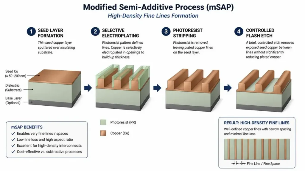
mSAP PCB Manufacturing Process Sequence Diagram
The mSAP process normally combines thin copper preparation, photoresist imaging, selective copper plating, resist stripping, flash etching, inspection, and electrical verification.
How Does Thin Copper Enable mSAP PCB Fine Lines?
The starting copper layer is much thinner than the copper foil normally used for conventional subtractive circuit formation.
A thinner seed layer reduces the amount of copper that must be removed between adjacent conductors during the final flash-etch step. This reduces the lateral material loss that contributes to trace undercut.
The practical benefit is not merely a smaller line width. It is better control over the relationship between:
trace width + trace height + sidewall profile + dielectric geometry.
These variables become increasingly important when controlled impedance and high-speed signal integrity are involved.
How Does LDI Improve mSAP PCB Pattern Accuracy?
Laser Direct Imaging (LDI) exposes the circuit image directly onto photoresist, eliminating the conventional phototool as the imaging intermediary.
For fine-line mSAP manufacturing, important parameters include:
- imaging resolution;
- registration accuracy;
- panel distortion;
- thermal expansion;
- fiducial recognition;
- exposure uniformity;
- layer-to-layer registration.
At Shenzhen Hongda Circuit, advanced LDI equipment is used as part of the fine-line imaging process. The engineering objective is not simply a high-resolution exposure number; it is repeatable registration under actual production conditions.
For example, PCBKR’s advanced manufacturing data includes SCREEN Ledia LDI capability with an engineering registration target of approximately ±8 μm on applicable production platforms, while tighter advanced-process figures must be treated according to the specific equipment, construction, and qualification route.
This distinction matters because machine resolution is not the same as finished-board registration capability.
How Does Copper Plating Build the mSAP Circuit?
After imaging and developing, exposed areas become the locations where copper is selectively deposited.
The plating process must control:
- copper thickness;
- current density;
- additive chemistry;
- panel-edge effects;
- feature density;
- plating distribution;
- via filling where applicable;
- copper grain structure.
For an mSAP PCB, copper plating is therefore both a dimensional process and a reliability process.
Too little copper can reduce conductor cross-section and reliability.
Too much copper can alter the intended geometry and narrow the process window.
Why Is Flash Etching the Critical Step in mSAP PCB Manufacturing?
Flash etching removes the remaining thin seed copper between plated conductors.
This is one of the most important process-control points in mSAP PCB manufacturing.
If the etch is insufficient:
- residual copper may remain;
- shorts may occur;
- isolation may fail.
If the etch is excessive:
- conductor width may decrease;
- sidewalls may become more aggressive;
- copper cross-section may be reduced;
- impedance may shift.
The manufacturing objective is therefore a controlled etch window rather than simply “fast etching.”
What Is the Difference Between mSAP PCB and Conventional Subtractive PCB Manufacturing?
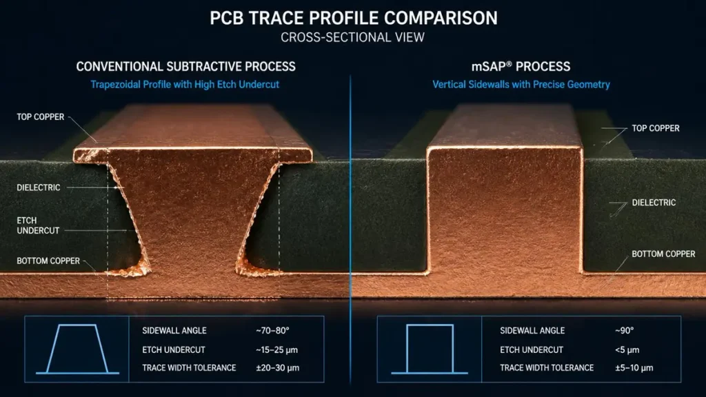
PCB Trace Profile Cross-Section: Conventional Subtractive vs. mSAP
The primary difference is how circuit copper is formed.
| Manufacturing Factor | Conventional Subtractive | mSAP PCB |
|---|---|---|
| Starting copper | Relatively thick foil | Thin copper seed/foil |
| Circuit formation | Remove unwanted copper | Plate required copper |
| Final seed removal | Not applicable in the same manner | Controlled flash etch |
| Etch undercut | Important limitation | Reduced |
| Fine-line potential | More limited | Higher |
| Process complexity | Lower | Higher |
| Process-control requirement | Moderate | High |
| Typical application | Standard PCB | Fine-line HDI/UHDI |
| Cost | Lower for suitable designs | Higher process complexity |
| Key risk | Etch geometry | Imaging, plating and flash-etch interaction |
Traditional subtractive processing inherently produces lateral etching because the etchant attacks exposed copper from more than one direction. Sierra Circuits identifies this undercut as one reason additive approaches become increasingly useful as line widths fall below approximately 2 mil.
The important engineering conclusion is:
mSAP does not make conventional PCB manufacturing obsolete. It expands the manufacturing process window when conventional etching becomes difficult to control.
What Is the Difference Between mSAP and SAP PCB Manufacturing?
Both mSAP and SAP are semi-additive technologies, but their starting structures and process architectures differ.
| Factor | Subtractive | mSAP | SAP |
|---|---|---|---|
| Starting copper | Relatively thick foil | Thin copper | Very thin seed layer |
| Main circuit formation | Etching | Pattern plating + flash etch | Pattern plating |
| Fine-line capability | Standard | Advanced | Ultra-fine |
| Process complexity | Lower | High | Very high |
| Typical use | Standard PCB | HDI/UHDI | Substrate/RDL-type applications |
| Cost | Lower | Higher | Higher still |
| Manufacturing environment | Conventional PCB | Advanced PCB | Substrate-oriented |
mSAP is often a practical bridge between conventional PCB fabrication and substrate-like manufacturing.
That makes it particularly relevant when a design requires significantly tighter geometries but does not necessarily justify the full process complexity of a substrate-oriented SAP flow.
What Line Width and Spacing Can an mSAP PCB Achieve?
This question requires more engineering context than a single minimum number.
An mSAP supplier may advertise a minimum line/space capability, but procurement teams should always ask what conditions apply to that number.
What Does 20/20 μm mSAP PCB Capability Actually Mean?
A 20/20 μm specification means approximately:
- 20 μm conductor width;
- 20 μm conductor spacing.
But the number alone does not tell the buyer whether the capability applies to:
- isolated features;
- dense routing;
- outer layers;
- inner build-up layers;
- a specific copper thickness;
- a specific dielectric;
- prototype quantities;
- pilot production;
- mass production.
Therefore:
Minimum line/space is a process capability statement, not automatically a production qualification statement.
PCBKR’s engineering approach is to distinguish design targets, engineering qualification, and production-qualified capability rather than presenting all three as one number.
Why Is Production-Qualified mSAP PCB Capability More Important Than Minimum Capability?
A supplier may successfully manufacture a small number of extremely fine-line test structures while achieving a very different result in continuous production.
Production qualification must consider:
- panel size;
- copper distribution;
- line density;
- material system;
- layer count;
- registration;
- plating distribution;
- etch window;
- inspection;
- yield;
- repeatability.
A useful procurement specification should therefore read more like:
20/20 μm line/space on specified mSAP layers, material system and copper thickness, subject to documented production qualification.
rather than simply:
Minimum line/space: 20/20 μm.
This distinction is one of the most important gaps between marketing-oriented capability tables and real manufacturing qualification.
How Does mSAP PCB Technology Improve HDI Routing?
mSAP is particularly valuable when HDI designs require dense routing around fine-pitch components.
It can support:
- microvia escape;
- stacked and staggered microvias;
- via-in-pad;
- fine-pitch BGA escape;
- Any-Layer HDI;
- higher routing density;
- smaller board footprints.
The relationship can be summarized as:
Smaller trace geometry → more routing channels → greater escape density → potential layer/board-size reduction.
But mSAP should be evaluated together with the complete HDI structure.
A 20 μm line/space capability does not compensate for poor:
- microvia registration;
- dielectric control;
- copper filling;
- lamination;
- via-to-pad alignment.
How Does mSAP Affect Controlled Impedance?
mSAP can improve conductor geometry control because it reduces the degree of trace undercut associated with conventional subtractive etching.
However, mSAP does not automatically guarantee controlled impedance.
Actual impedance depends on:
- trace width;
- copper thickness;
- trace profile;
- dielectric thickness;
- dielectric constant;
- reference-plane spacing;
- copper roughness;
- resin distribution;
- layer registration.
For high-speed applications, the correct engineering workflow is:
Material selection → stackup design → trace geometry → fabrication → impedance coupon → TDR verification.
IPC identifies IPC-2141 as a controlled-impedance/high-speed design reference and IPC-2226 as the sectional design standard for HDI printed boards.
What Materials Are Suitable for mSAP PCB Manufacturing?
Material selection should be driven by the electrical, thermal, mechanical and manufacturing requirements of the final product.
Potential material categories include:
- conventional high-Tg FR-4;
- low-loss laminates;
- high-speed materials;
- thin dielectric build-up materials;
- high-frequency/RF materials;
- advanced HDI dielectric systems.
For high-speed applications, buyers should review:
| Material Parameter | Why It Matters |
|---|---|
| Dk | Impedance and propagation delay |
| Df | Signal loss |
| Tg | Thermal reliability |
| CTE | Dimensional/reliability behavior |
| Copper roughness | High-frequency loss |
| Resin content | Dielectric geometry |
| Thickness tolerance | Impedance consistency |
| Availability | Lead time and supply continuity |
IPC-4101 covers base materials for rigid and multilayer printed boards, while IPC also maintains IPC-4103 for high-speed/high-frequency base materials.
For an mSAP RFQ, the laminate should therefore be specified by an actual material designation and required electrical properties rather than simply “high-speed material.”
What Are the Biggest Manufacturing Pain Points for mSAP PCB?
The biggest challenge is not making one fine trace.
It is controlling multiple small process variations simultaneously without allowing them to accumulate into yield loss or electrical variation.
Why Is Flash-Etch Control a Major mSAP PCB Risk?
The seed layer must be removed between conductors while protecting the plated traces.
The process window becomes increasingly narrow as geometry decreases.
Potential defects include:
- residual copper;
- shorts;
- trace thinning;
- line-width variation;
- sidewall deformation.
Why Is LDI Registration Critical for mSAP PCB?
At fine geometries, a small registration error represents a large percentage of the intended feature size.
For example, a 3 μm positional error is:
- 15% of a 20 μm feature;
- 12% of a 25 μm feature;
- 10% of a 30 μm feature.
This illustrates why a supplier should report registration capability together with the actual construction rather than quoting imaging resolution alone.
Why Is Copper Plating Uniformity Important?
Copper thickness changes the conductor cross-section.
This can affect:
- resistance;
- impedance;
- current capacity;
- trace profile;
- reliability.
The plating process must therefore control both average thickness and distribution across the panel.
Why Is Registration Between mSAP and Microvias Difficult?
Fine-line traces and microvias must align within a much smaller process window.
The critical interfaces include:
microvia → capture pad → fine-line trace
A supplier therefore needs coordinated control of:
- laser drilling;
- LDI;
- lamination;
- material shrinkage;
- registration compensation;
- copper plating.
How Do Modern PCB Manufacturing Technologies Improve mSAP PCB Production?
mSAP performance increasingly depends on an integrated manufacturing platform rather than one individual machine.
How Does Advanced LDI Support mSAP PCB Manufacturing?
Advanced LDI supports:
- direct digital imaging;
- high-resolution pattern formation;
- registration compensation;
- panel distortion mapping;
- fine-line patterning.
PCBKR uses SCREEN Ledia LDI technology within its advanced fine-line manufacturing platform.
How Does UV and CO₂ Laser Drilling Support mSAP HDI?
Laser drilling is used for:
- blind microvias;
- stacked microvias;
- staggered microvias;
- via-in-pad structures;
- fine-pitch interconnections.
PCBKR’s manufacturing platform includes Mitsubishi UV/CO₂ laser drilling for HDI structures, with process capability determined by the specific material, hole diameter, depth, copper construction and qualification condition.
How Does Precision Lamination Affect mSAP PCB Reliability?
As build-up structures become thinner and more complex, lamination influences:
- dielectric thickness;
- registration;
- void formation;
- resin flow;
- warpage;
- interlayer adhesion.
PCBKR uses controlled lamination equipment, including LAUFFER systems, for advanced multilayer and HDI constructions.
The objective is not merely higher pressure or temperature. It is a repeatable lamination cycle matched to the material system.
How Do AOI, X-Ray and Electrical Testing Support mSAP PCB Quality?
No single inspection technology can detect every mSAP failure mode.
A risk-based inspection strategy can combine:
- AOI;
- X-ray;
- microsection;
- dimensional measurement;
- electrical testing;
- impedance testing;
- reliability testing.
IPC-A-600 defines acceptability criteria for externally and internally observable PCB conditions, while IPC-6012 establishes qualification and performance requirements for rigid printed boards, including multilayer structures with blind, buried and microvias.
How Should mSAP PCB Quality Be Verified?
A serious mSAP qualification program should connect every important process parameter with a verification method.
| Manufacturing Risk | Process Control | Verification |
|---|---|---|
| Fine-line imaging | LDI registration | Optical measurement |
| Trace-width variation | Pattern plating + flash etch | Dimensional inspection |
| Residual copper | Flash etch | AOI / microscopy |
| Copper thickness variation | Plating control | Cross-section / thickness measurement |
| Microvia misregistration | Laser + registration compensation | X-ray / cross-section |
| Via reliability | Copper filling + lamination | Microsection / reliability test |
| Impedance variation | Stackup + geometry control | TDR |
| Internal defects | Lamination process | X-ray / microsection |
IPC also provides test coupon guidance for structural integrity, registration and other production verification purposes.
The important procurement principle is:
Do not ask only what equipment a supplier owns. Ask which defect each process is designed to control and how that control is verified
How Does mSAP PCB Manufacturing Affect Cost?
mSAP normally costs more than conventional subtractive fabrication because it requires:
- thin copper materials;
- additional process steps;
- tighter process control;
- advanced imaging;
- controlled plating;
- flash etching;
- additional metrology;
- more engineering review;
- tighter quality control.
However, the correct cost comparison is not:
mSAP PCB price vs conventional PCB price.
It is:
Total product cost with mSAP vs total product cost with conventional fabrication.
Can mSAP Reduce Total PCB Cost?
Potentially, yes.
A successful mSAP design may reduce:
- layer count;
- board area;
- routing complexity;
- escape-routing constraints;
- redesign cycles;
- package-to-PCB interconnection difficulty.
For example, if a denser routing architecture allows the engineering team to eliminate layers, the higher fabrication cost of selected mSAP layers may be offset by reductions elsewhere in the stackup.
Therefore, mSAP should be evaluated using a total-cost-of-design and manufacturing model, not only a fabrication-unit-price comparison.
When Should Engineers Choose mSAP PCB Instead of Conventional PCB?
mSAP becomes more attractive when one or more of the following conditions apply:
- conventional line/space cannot meet the design;
- BGA escape is highly constrained;
- board miniaturization is important;
- HDI routing density is high;
- layer reduction has significant value;
- fine-line controlled impedance is required;
- the design uses advanced microvia structures.
Conventional subtractive processing may remain preferable when:
- line/space requirements are relatively relaxed;
- board area is available;
- layer count is not a major constraint;
- cost sensitivity is high;
- the design does not require advanced HDI density.
SAP may become appropriate when the required geometry moves beyond the practical mSAP process window.
The correct choice is therefore application-dependent rather than technology-dependent.
How Should Buyers Qualify an mSAP PCB Manufacturer?
A procurement team should request evidence instead of accepting a minimum-feature marketing number.
What Should You Ask an mSAP PCB Manufacturer?
- What is your production-qualified line/space?
- What copper thickness applies to that capability?
- Which materials are qualified?
- Which PCB layers use mSAP?
- What registration capability is achieved on actual production panels?
- How is flash-etch uniformity controlled?
- How is plating uniformity verified?
- Can you provide cross-section data?
- What microvia structures are qualified?
- Can the same process move from prototype to volume production?
- What IPC acceptance criteria are applied?
- How are process changes controlled?
- What inspection reports accompany production lots?
- What information is required for an engineering RFQ?
This qualification process is more meaningful than asking:
“Can you make 10 μm lines?”
What Is the Difference Between mSAP PCB Capability and Production Qualification?
This distinction should be explicitly written into the purchasing specification.
Design Capability
The geometry the engineering team wants to use.
Demonstrated Capability
A geometry successfully produced during engineering or qualification trials.
Production-Qualified Capability
A geometry repeatedly manufactured under defined production conditions with documented process control and acceptable yield.
These three values may be different.
For example:
| Capability Type | Example |
|---|---|
| Design target | 15/15 μm |
| Engineering qualification | 15/15 μm |
| Production-qualified target | 20/20 μm |
| Standard production | 25/25 μm |
The exact values must be established for the specific material, layer construction, copper thickness, panel format and quality requirements.
This is a more useful way to evaluate an mSAP PCB supplier than comparing isolated “minimum line/space” claims.
Can mSAP PCB Production Scale From Prototype to Mass Production?
Yes, but prototype success does not automatically prove mass-production readiness.
A controlled NPI pathway should include:
Prototype → Engineering Validation → Pilot Run → Process Qualification → Mass Production
At each stage, the supplier should evaluate:
- registration;
- line/space;
- copper thickness;
- plating distribution;
- flash-etch window;
- microvia reliability;
- impedance;
- yield;
- material availability;
- inspection results.
This is particularly important for AI, optical, automotive, medical and other applications where a production change can trigger a costly qualification cycle.
What Standards Should Be Considered for mSAP PCB Manufacturing?
mSAP itself should not be treated as a standalone replacement for the applicable PCB performance standards.
Depending on the construction and end application, relevant IPC references can include:
- IPC-6012F — Qualification and Performance Specification for Rigid Printed Boards;
- IPC-A-600 — Acceptability of Printed Boards;
- IPC-2221 — Generic Standard on Printed Board Design;
- IPC-2226 — HDI printed board design;
- IPC-4101 — Base materials for rigid and multilayer printed boards;
- IPC-4103 — High-speed/high-frequency base materials;
- IPC-2141 — Controlled impedance and high-speed logic design.
IPC states that IPC-6012F establishes qualification and performance requirements for rigid printed boards, including multilayer boards with blind, buried and microvias.
IPC also identifies IPC-2226 as the sectional design standard for HDI printed boards.
The applicable standard, revision, class and acceptance criteria should always be agreed between the PCB manufacturer and customer for the specific product.
How Does Shenzhen Hongda Circuit Support mSAP PCB Manufacturing?
Shenzhen Hongda Circuit Technology Co., Ltd. (PCBKR) combines fine-line PCB fabrication with HDI, laser drilling, controlled impedance, advanced inspection and engineering review.
Our relevant manufacturing technologies include:
- advanced LDI imaging;
- mSAP fine-line processing;
- UV/CO₂ laser drilling;
- precision microvia fabrication;
- sequential lamination;
- automated copper plating;
- AOI;
- X-ray inspection;
- electrical testing;
- controlled-impedance verification;
- cross-section and reliability analysis.
PCBKR’s equipment platform includes SCREEN Ledia LDI, Mitsubishi UV/CO₂ laser systems, and LAUFFER lamination equipment for applicable advanced PCB constructions.
The engineering principle is simple:
The equipment must be connected to a measurable manufacturing result.
For mSAP PCB production, that means controlling the chain:
Material → Imaging → Registration → Plating → Flash Etching → Inspection → Electrical Verification → Reliability
rather than presenting equipment names as a substitute for process qualification.
What Information Should You Include in an mSAP PCB RFQ?
A complete RFQ allows the manufacturer to evaluate manufacturability before quoting.
What PCB Data Should Be Included?
Provide:
- Gerber or ODB++ files;
- drill files;
- fabrication drawing;
- stackup;
- layer count;
- board dimensions;
- finished copper thickness;
- minimum line/space;
- microvia diameter;
- via structure;
- via-in-pad requirements;
- controlled-impedance table;
- surface finish;
- solder mask;
- material specification.
What Commercial Data Should Be Included?
Also provide:
- prototype quantity;
- pilot quantity;
- annual volume;
- target production date;
- packaging requirements;
- inspection requirements;
- certification requirements;
- delivery destination;
- qualification requirements.
This allows PCBKR engineers to distinguish between:
design intent → manufacturability → production capability → commercial quotation.
Why Should You Request an mSAP PCB Manufacturing Review Before Ordering?
Fine-line PCB fabrication should be reviewed before production rather than after a manufacturing problem appears.
A pre-production review can identify:
- line/space risks;
- registration limitations;
- unsuitable copper thickness;
- microvia conflicts;
- impedance risks;
- material availability issues;
- stackup problems;
- panelization concerns;
- unrealistic lead-time expectations.
For advanced PCB programs, early DFM can prevent expensive redesigns and qualification delays. IPC itself describes DFM as an important product-development step and provides DFM guidance based on several IPC design and performance standards.
What Makes mSAP PCB Manufacturing Difficult?
The hardest part of mSAP manufacturing is not achieving one extremely small feature.
The real challenge is maintaining fine-line geometry, registration, copper distribution, etch control, dielectric consistency and reliability simultaneously across a production panel and across repeated manufacturing lots.
That is why the most meaningful supplier question is not:
“What is your smallest line/space?”
It is:
“What geometry can you repeatedly manufacture under defined production conditions, and what evidence can you provide?”
That is the question experienced PCB engineers and procurement teams should ask.
How Can You Request an mSAP PCB Quote From PCBKR?
If your design requires fine-line HDI, mSAP, microvia, fine-pitch BGA escape, controlled impedance or high-density routing, send your PCB data to Shenzhen Hongda Circuit Technology Co., Ltd.
PCBKR’s engineering team can review:
- mSAP manufacturability;
- line/space requirements;
- HDI structure;
- microvia design;
- stackup;
- material selection;
- impedance requirements;
- production risks;
- prototype and volume requirements.
Request an mSAP PCB Manufacturing Review
Website: www.pcbkr.com
Email: pcb@pcbkr.com
mSAP PCB Manufacturing FAQ
What does mSAP mean in PCB manufacturing?
mSAP means Modified Semi-Additive Process. It forms PCB conductors by selectively plating copper over a thin starting copper layer and then removing the remaining seed layer through controlled flash etching.
What is an mSAP PCB used for?
mSAP PCBs are used when conventional PCB fabrication cannot reliably provide the required routing density or fine-line geometry. Applications can include advanced HDI, fine-pitch BGA, optical communication, high-speed electronics, automotive electronics, medical electronics and miniaturized devices.
What is the difference between mSAP and subtractive PCB manufacturing?
Subtractive manufacturing starts with relatively thick copper and removes unwanted copper. mSAP starts with a much thinner copper layer, selectively plates the required conductors and then removes the remaining seed copper. This can reduce etch undercut and support finer circuit geometries.
What is the difference between mSAP and SAP?
Both are semi-additive technologies, but mSAP normally starts with a thin laminated copper layer, while SAP uses an even thinner seed layer and is generally associated with more substrate-like ultra-fine structures. The appropriate process depends on the required geometry and application.
Can mSAP PCB manufacturing support HDI?
Yes. mSAP is particularly useful for HDI structures because fine-line routing can be combined with laser-drilled microvias, stacked or staggered vias and fine-pitch BGA escape.
Can mSAP PCB improve controlled impedance?
mSAP can provide more controlled conductor geometry than conventional subtractive etching, but impedance depends on the complete stackup, trace width, copper thickness, dielectric properties and reference-plane geometry. TDR verification should be used when controlled impedance is specified.
Is mSAP PCB manufacturing more expensive?
Generally, mSAP involves more process control and advanced equipment than conventional subtractive fabrication, so its fabrication cost can be higher. However, mSAP may reduce total product cost when it enables fewer layers, a smaller board, simpler routing or fewer redesigns.
What is the most important mSAP PCB manufacturing challenge?
One of the most important challenges is maintaining a sufficiently wide and stable process window across imaging, plating and flash etching. Fine-line manufacturing becomes increasingly sensitive to small dimensional variations.
What should I ask an mSAP PCB manufacturer?
Ask about production-qualified line/space, copper thickness, materials, registration, plating uniformity, flash-etch control, microvia capability, inspection methods, reliability testing, production yield and prototype-to-volume scalability.
Does a supplier’s minimum line/space equal its mass-production capability?
No. A minimum demonstrated feature should not automatically be interpreted as a production-qualified capability. Buyers should ask for the material, layer, copper thickness, panel size, process conditions and production evidence associated with the quoted geometry.
What standards apply to mSAP PCB manufacturing?
The applicable requirements depend on the PCB construction and application. Common IPC references include IPC-6012F for rigid PCB performance, IPC-A-600 for acceptability, IPC-2221 for general design, IPC-2226 for HDI design, and IPC-4101/4103 for applicable base materials.
What files are required for an mSAP PCB RFQ?
A complete RFQ should normally include Gerber or ODB++ data, drill files, fabrication drawings, stackup, material requirements, copper thickness, line/space, microvia information, impedance requirements, quantity and delivery requirements.
Can PCBKR support mSAP PCB prototypes and production?
Shenzhen Hongda Circuit Technology Co., Ltd. provides PCB engineering and manufacturing services covering advanced HDI, fine-line processing, microvia fabrication, controlled impedance and production requirements. The exact mSAP capability should be confirmed against the customer’s stackup, materials, geometry, volume and qualification requirements.
Author & Engineering Perspective
David Chen — PCB Manufacturing & Engineering https://www.linkedin.com/in/pcbcoming
David Chen has more than ten years of experience in PCB manufacturing, PCBA engineering, process optimization, high-precision fault analysis and reliability testing. His technical focus includes advanced PCB fabrication, complex circuit structures, manufacturing process control and engineering evaluation of high-density interconnect technologies.
The manufacturing recommendations in this article are written from a PCB engineering and procurement perspective: a capability claim should be connected to a defined process condition, measurable parameter and appropriate verification method.
For advanced PCB projects, the objective is not simply to manufacture the smallest possible feature. It is to manufacture the required geometry consistently, reliably and economically at the intended production volume.
Shenzhen Hongda Circuit Technology Co., Ltd. (PCBKR)
Website: www.pcbkr.com
Email: pcb@pcbkr.com