IC Substrate Manufacturing & Design Guide
What Is an IC Substrate?
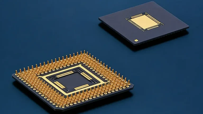
An IC substrate is a high-density package interconnect between a semiconductor die and its package or system PCB, combining fine-line routing, microvias, controlled registration, mechanical support and package-level reliability.
The basic electrical path is:
Semiconductor die → IC substrate → package interconnection → system PCB
An IC substrate therefore sits at a different engineering level from a conventional FR-4 PCB.
A conventional PCB primarily connects components at the system level. An IC substrate must translate extremely dense semiconductor I/O into a package-level interconnection structure that can ultimately connect to the motherboard.
This requires a combination of:
- Fine-line copper routing
- Build-up dielectric layers
- Laser-drilled microvias
- Stacked or staggered microvias
- Via-in-pad structures
- Flip-chip or wire-bond interfaces
- Tight layer-to-layer registration
- Controlled copper distribution
- Warpage management
- Electrical and reliability verification
The manufacturing challenge is not simply achieving one very small feature.
It is maintaining several small features simultaneously and repeatedly across the complete process sequence.
That distinction matters when evaluating an IC substrate manufacturer.
A supplier may be technically capable of producing a particular minimum line/space under a controlled test condition while not necessarily being qualified to manufacture a customer’s complete package architecture at production volume.
For procurement, the relevant question is therefore:
Can the supplier repeatedly manufacture this exact structure within the required dimensional, electrical, mechanical and reliability window?
That is the question this guide addresses.
Why Is an IC Substrate Different From a Conventional PCB?
An IC substrate operates between semiconductor packaging and system-level PCB interconnection, so its manufacturing priorities shift toward I/O density, fine-line routing, microvia reliability, registration and package warpage.
| Engineering Factor | Conventional PCB | HDI PCB | IC Substrate |
|---|---|---|---|
| Main function | System interconnection | High-density system interconnection | Die/package interconnection |
| Routing density | Medium–high | High | Very high |
| Microvias | Application dependent | Common | Fundamental |
| Build-up structure | Application dependent | Common | Common |
| Fine-line requirement | Application dependent | High | Very high |
| Registration sensitivity | High | Very high | Extremely high |
| Warpage sensitivity | Moderate–high | High | Very high |
| Package interface | Indirect | Usually indirect | Direct |
| Primary yield concern | Board defects | Density/reliability | Fine features + package reliability |
The difference becomes obvious in a flip-chip package.
A die may contain a very large number of closely spaced I/O connections. Those connections must escape through the substrate without violating:
- minimum conductor spacing;
- pad geometry;
- dielectric thickness;
- microvia landing tolerance;
- copper-density constraints;
- signal-integrity requirements;
- package warpage limits.
This creates a manufacturing problem that cannot be solved simply by increasing PCB layer count.
More layers do not automatically provide better substrate performance.
The layer structure, dielectric thickness, via architecture, copper distribution and package geometry must work together.
What Are the Main Types of IC Substrates?
Common organic IC substrate structures include BT-based substrates, ABF build-up substrates, FC-BGA and FC-CSP substrates, wire-bond substrates and SiP-related structures, while glass-core and other advanced architectures are emerging for high-density packaging.
What Is a BT IC Substrate?
BT resin systems are used in package substrates where electrical performance, dimensional stability, thermal behavior and manufacturability must be balanced.
Typical applications can include:
- CSP
- FC-CSP
- memory packages
- RF packages
- consumer semiconductor packages
- SiP structures
What Is an ABF IC Substrate?
ABF means Ajinomoto Build-up Film.
ABF is used as a build-up dielectric in high-density package-substrate structures and is particularly associated with advanced processor and FC-BGA applications.
Current industry analysis describes ABF as a build-up film positioned between silicon dies such as CPU/GPU devices and the PCB, providing the dielectric structure needed for dense multilayer routing and microvias.
What Is an FC-BGA Substrate?
An FC-BGA substrate connects a flip-chip die to a package ball array.
The manufacturing challenge is to transform a dense die-side bump pattern into a larger package-side interconnection array.
Critical parameters include:
- die size;
- bump pitch;
- I/O count;
- substrate thickness;
- build-up layer count;
- microvia structure;
- routing density;
- package warpage.
What Is an FC-CSP Substrate?
FC-CSP structures generally emphasize compact package dimensions, short interconnection paths and high-density routing.
What Is a Wire-Bond Substrate?
Wire-bond substrates use bond-pad structures rather than flip-chip bump connections, so the substrate design rules differ from FC-BGA architectures.
What Is a SiP Substrate?
System-in-package structures may integrate multiple dies, passive components, RF elements and other components in a single package.
That increases the importance of:
- component placement;
- electrical isolation;
- thermal paths;
- fine routing;
- power distribution;
- mechanical stability.
How Do You Choose Between ABF and BT IC Substrates?
ABF or BT should be selected according to package architecture, I/O density, routing requirements, thermal-mechanical behavior, reliability targets and production economics rather than by assuming that one material is universally better.
| Design Factor | BT | ABF |
|---|---|---|
| Package density | Moderate–high | High–very high |
| Fine-line routing | Application dependent | Strong fit |
| Build-up structure | Available | Core application |
| FC-BGA | Possible | Strong fit |
| FC-CSP | Common | Application dependent |
| High-I/O processor | Application dependent | Strong fit |
| Process complexity | High | Very high |
| Cost sensitivity | Often favorable | Higher process complexity |
A procurement engineer should provide the supplier with at least:
- Die dimensions
- Package outline
- I/O count
- Bump pitch
- Ball pitch
- Target line/space
- Microvia diameter
- Layer count
- Substrate thickness
- Warpage requirement
- Reliability requirements
- Annual volume
A material comparison without these parameters is incomplete.
For example, changing from BT to ABF may improve the routing solution for a high-I/O package, but the decision also changes the manufacturing process, dielectric behavior, lamination conditions, laser response and qualification requirements.
What Materials Are Used in IC Substrate Manufacturing?
IC substrates may use BT resin, ABF build-up films, specialized dielectric materials, copper foils and structural core materials, with glass and other advanced core concepts being developed for future high-density packaging.
Material selection should consider:
- dielectric constant;
- dielectric loss;
- Tg;
- CTE;
- Z-axis expansion;
- modulus;
- moisture absorption;
- copper adhesion;
- laser processability;
- dimensional stability;
- thermal cycling behavior.
For high-speed package routing, dielectric loss can become important.
For large packages, CTE mismatch and mechanical modulus can become dominant.
For fine-line structures, dielectric thickness and surface condition affect laser drilling, metallization and build-up accuracy.
Therefore, the correct engineering question is not:
“Which material has the lowest Dk?”
It is: “Which material provides the required electrical, mechanical, thermal and manufacturing window for the complete package?”
How Is an IC Substrate Manufactured?
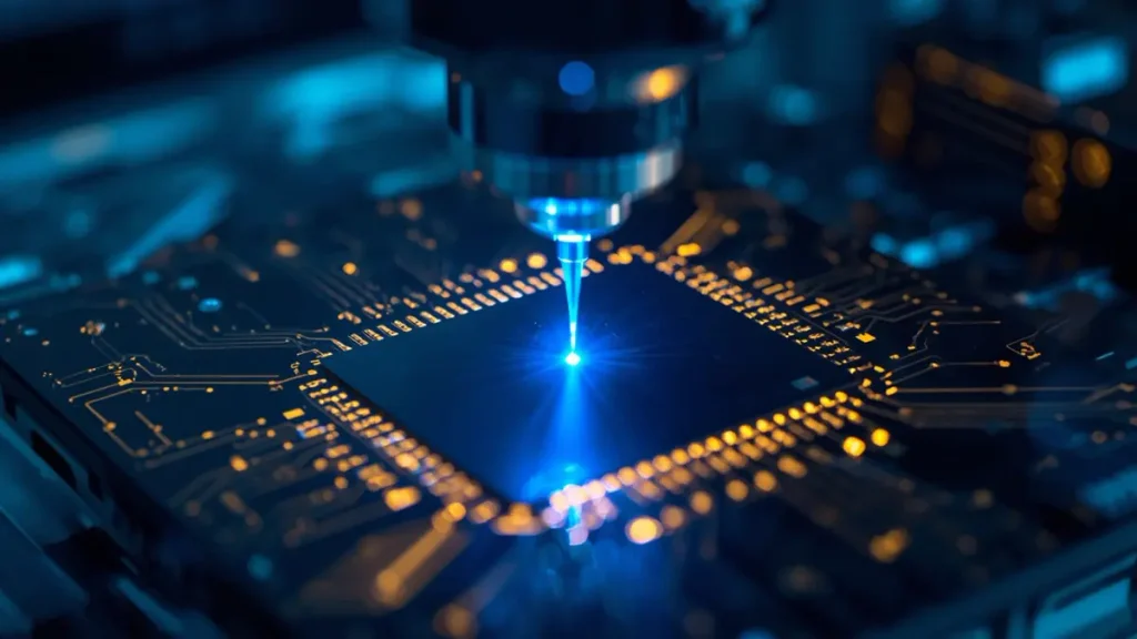
High-Precision UV Laser Drilling Microvias on IC Substrate
IC substrate manufacturing combines core preparation, dielectric build-up, laser drilling, desmear, seed metallization, SAP or mSAP patterning, copper plating, microvia filling, sequential lamination, surface finishing and multi-stage inspection.
A simplified process flow is:
Core preparation
→ Dielectric build-up
→ Laser drilling
→ Desmear
→ Seed copper
→ Photo imaging
→ SAP/mSAP patterning
→ Electrolytic copper
→ Microvia filling
→ Sequential lamination
→ Registration verification
→ Surface finish
→ AOI / X-ray / electrical inspection
→ Reliability verification
The difficulty is not any single process.
The difficulty is cumulative dimensional control.
Suppose an individual layer has a small registration error. That error may be acceptable by itself. After several build-up cycles, however, the total positional relationship between die-side pads, microvias and package-side connections becomes increasingly important.
This is why an experienced IC substrate manufacturing process must control:
- material movement;
- imaging;
- laser drilling;
- plating;
- lamination;
- registration;
- copper distribution;
- inspection.
Why Are SAP and mSAP Important for IC Substrate Manufacturing?
SAP and mSAP provide a fine-line manufacturing route in which conductor geometry is formed by selective copper build-up rather than relying solely on conventional subtractive copper etching.
In conventional subtractive processing, a relatively thick copper layer is etched away to leave the circuit.
As line width decreases, the relationship between:
copper thickness / line width / etch factor / sidewall geometry
becomes increasingly difficult to control.
mSAP uses a different sequence:
thin seed copper → photo patterning → selective copper build-up → seed removal
This provides greater flexibility for fine copper structures.
PCBKR’s current mSAP production information identifies continuous mSAP production since 2024, with a 2026 production target of 20/20 μm line/space in volume and 8/8 μm qualified capability for substrate-like PCB structures. These numbers should be treated as process-specific qualified capability rather than a universal specification for every IC substrate architecture.
That qualification distinction is important.
A minimum feature size is not automatically a mass-production specification for every design.
The actual process window depends on:
- material;
- copper thickness;
- panel size;
- feature density;
- dielectric thickness;
- via architecture;
- yield target;
- inspection requirements.
How Does LDI Improve Fine-Line IC Substrate Manufacturing?
Laser Direct Imaging provides digitally controlled photo-patterning that helps improve fine-line imaging repeatability and layer registration without relying on conventional phototools.
PCBKR’s published mSAP information identifies high-resolution LDI with approximately ±1.5 μm registration accuracy for the relevant process platform.
The practical value of LDI is not simply resolution.
Consider a fine-line pattern with a nominal 20 μm conductor.
If imaging, plating, etching compensation and registration each introduce uncontrolled variation, the final conductor geometry can move outside the intended process window.
LDI helps by allowing:
- digital pattern generation;
- exposure compensation;
- registration correction;
- repeatable image transfer.
For dense package routing, this becomes important where many small features must remain aligned across sequential build-up layers.
How Does Laser Drilling Affect IC Substrate Reliability?
Laser drilling controls microvia diameter, depth, taper, dielectric removal and thermal influence, all of which affect subsequent metallization, via filling and reliability.
PCBKR’s published manufacturing information identifies Mitsubishi UV/CO₂ laser processing for microvia structures and advanced picosecond/femtosecond laser processing for specialized microfabrication.
Why Does Laser Type Matter?
CO₂ and UV lasers interact differently with dielectric materials.
The engineering objective is not merely to drill the smallest possible hole.
A microvia must also have:
- clean dielectric removal;
- controlled bottom geometry;
- acceptable taper;
- good copper interface;
- reliable metallization;
- reliable filling;
- adequate thermal-cycle performance.
An extremely small hole that cannot be reliably metallized is not a successful manufacturing process.
What Are the Most Important IC Substrate Design Rules?
The critical design parameters include line/space, microvia diameter, pad geometry, dielectric thickness, via stacking, layer registration, copper distribution, package pitch and warpage.
| Parameter | Engineering Question |
|---|---|
| Line/space | Can final copper geometry remain within tolerance? |
| Microvia | Can the laser create a reliable interconnect? |
| Via pad | Is landing tolerance adequate? |
| Dielectric thickness | Is the laser/process window stable? |
| Stackup | Is the mechanical structure balanced? |
| Registration | Can all build-up layers align? |
| Copper distribution | Is thermal/mechanical balance acceptable? |
| Bump pitch | Can the escape routing be manufactured? |
| Package size | Does the geometry increase warpage risk? |
| Warpage | Can package assembly remain stable? |
A common engineering mistake is to begin the design review with the smallest advertised feature.
A better approach is:
Package geometry → I/O escape → via architecture → layer structure → material → process capability → reliability
This sequence helps prevent a design from becoming theoretically impressive but difficult to manufacture.
What Causes IC Substrate Warpage?
IC substrate warpage is primarily influenced by CTE mismatch, copper distribution, asymmetric stackups, dielectric behavior, resin shrinkage, lamination history, package dimensions and thermal cycling.
Typical contributors include:
- asymmetric copper distribution;
- unequal dielectric thickness;
- resin shrinkage;
- CTE mismatch;
- large package dimensions;
- thermal gradients;
- uneven copper density;
- curing conditions;
- repeated lamination cycles.
Consider a large FC-BGA substrate.
One region may contain dense power and ground copper while another region contains mostly dielectric and signal routing.
The average copper percentage may look acceptable.
The local copper distribution, however, can still generate mechanical imbalance.
That is why copper balancing should be considered during stackup and panel design rather than after manufacturing.
How Does Controlled Lamination Affect IC Substrate Dimensional Stability?
Controlled lamination helps manage resin flow, dielectric thickness, pressure distribution and thermal expansion during sequential build-up.
PCBKR’s published equipment information identifies LAUFFER lamination equipment within its advanced manufacturing platform.
For high-density structures, lamination affects:
- dielectric thickness;
- layer-to-layer registration;
- resin distribution;
- panel flatness;
- dimensional stability;
- via landing accuracy.
The engineering principle is straightforward:
A fine-line process cannot compensate indefinitely for unstable upstream dimensions.
If dielectric thickness and panel geometry move unpredictably during lamination, later laser and imaging processes inherit that variation.
What Are the Most Difficult Manufacturing Problems for IC Substrates?
The hardest manufacturing problems are interactions between fine-line formation, microvia reliability, registration, copper plating, material movement, warpage and production yield.
Fine-Line Variation
At 20 μm line/space, a 2 μm dimensional change represents 10% of the nominal feature width.
That is why process capability matters more as feature size decreases.
Microvia Reliability
Potential failure mechanisms include:
- incomplete desmear;
- poor copper adhesion;
- voids;
- insufficient copper fill;
- stress concentration;
- thermal fatigue.
Registration Drift
Sequential build-up increases the importance of layer-to-layer alignment.
Plating Variation
Copper thickness influences:
- conductor width;
- spacing;
- resistance;
- via reliability;
- surface geometry.
PCBKR’s published mSAP information identifies approximately ±3% plating uniformity for its relevant large-panel plating process.
Warpage
A substrate can pass electrical inspection and still create package assembly problems if its mechanical geometry falls outside the customer’s assembly window.
This is why warpage should be treated as an engineering parameter rather than merely a final inspection result.
How Does PCBKR Control Copper Plating for Fine-Line Structures?
Shenzhen Hongda Circuit Technology uses automated plating technology for desmear, electroless copper and electrolytic copper processes, with published process information specifying approximately ±3% plating uniformity for the relevant mSAP route.
Copper plating has two competing requirements.
Too much copper growth can affect:
- line width;
- spacing;
- sidewall profile;
- impedance;
- shorts.
Too little copper can affect:
- resistance;
- current capacity;
- interconnect strength;
- via reliability.
For fine-line structures, plating therefore becomes part of dimensional control.
The process should be evaluated through:
seed thickness → current distribution → plating chemistry → copper thickness → pattern geometry → inspection
rather than by treating plating only as a conductivity operation.
How Are IC Substrates Inspected and Tested?
IC substrate inspection should combine optical inspection, X-ray, dimensional verification, cross-section analysis, electrical testing, material verification and application-specific reliability testing.
PCBKR’s published inspection platform includes:
- 3D X-ray;
- AOI;
- XRF;
- flying-probe testing;
- TDR;
- cross-section analysis.
| Inspection Method | Primary Purpose |
|---|---|
| AOI | Surface circuit defects |
| 3D X-ray | Hidden structures and internal defects |
| XRF | Coating/metal thickness verification |
| Flying probe | Electrical continuity/isolation |
| TDR | Controlled impedance where applicable |
| Cross-section | Physical construction verification |
| Dimensional inspection | Line/space and registration |
| Warpage measurement | Package assembly risk |
| Reliability testing | Long-term structural performance |
For procurement qualification, an AOI report alone is not sufficient.
A more useful qualification package can include:
material certificate + stackup + cross-section + dimensional report + electrical test + X-ray data + reliability data + lot traceability.
Why Is X-Ray Inspection Important for IC Substrate Manufacturing?
X-ray inspection provides non-destructive visibility into buried structures that cannot be evaluated reliably from the outer surface.
PCBKR’s published equipment information includes Nordson DAGE 3D X-ray inspection for internal structures.
X-ray inspection can help identify:
- internal voids;
- hidden interconnection problems;
- via-related anomalies;
- BGA-related defects;
- internal structural abnormalities.
However, X-ray and cross-section analysis serve different purposes.
X-ray identifies non-visible structures without destroying the sample.
Cross-section reveals the physical construction and helps establish root cause.
For failure analysis, both can be valuable.
What Causes IC Substrate Reliability Failures?
Reliability failures can originate from thermal-mechanical stress, microvia construction, copper fatigue, material mismatch, delamination, moisture and package warpage.
Common failure mechanisms include:
- microvia cracking;
- copper fatigue;
- interfacial delamination;
- resin cracking;
- pad separation;
- via-fill defects;
- thermal-cycle failure;
- warpage-related assembly failure.
A useful root-cause model is:
Material → Process → Structure → Test → Failure Mechanism
For example, if a microvia fails during thermal cycling, the engineering investigation should determine whether the failure initiated at:
- the copper interface;
- via barrel;
- via fill;
- target pad;
- dielectric interface;
- adjacent copper structure.
That information determines the corrective action.
How Much Does an IC Substrate Cost?
IC substrate cost depends on material, layer count, package size, fine-line geometry, microvia density, SAP/mSAP processing, panel utilization, testing, qualification, volume and manufacturing yield.
A useful cost model is:
Material + Process + Yield + Testing + NRE + Panel Utilization + Qualification + Logistics
Major Cost Drivers
| Cost Driver | Cost Impact |
|---|---|
| ABF vs BT | Material/process complexity |
| Layer count | More build-up and lamination |
| Fine-line geometry | Tighter process control |
| Microvia density | Laser/plating/inspection |
| SAP/mSAP | Specialized process |
| Package size | Panel utilization |
| Prototype volume | Limited economies of scale |
| Reliability testing | Qualification expense |
| Yield | Direct effective cost |
| Material availability | Schedule and procurement risk |
Two substrates with identical external dimensions can therefore have very different manufacturing costs.
A substrate requiring:
8/8 μm mSAP + stacked microvias + high-density build-up
is fundamentally different from one using:
25/25 μm routing + conventional HDI processing.
For this reason, a reliable IC substrate quotation should be based on actual design data rather than board area alone.
What Lead Time Should Buyers Expect for IC Substrate Manufacturing?
validation, qualification, pilot production or established mass production.
A useful schedule is:
Engineering review
→ DFM
→ Prototype
→ Qualification
→ Pilot
→ Production
Lead time is influenced by:
- ABF/BT material availability;
- stackup complexity;
- new process development;
- laser drilling;
- mSAP processing;
- inspection;
- reliability qualification;
- quantity;
- customer approval.
Therefore, a supplier that gives one universal “IC substrate lead time” without knowing the package architecture is not providing enough information for serious procurement planning.
How Should Buyers Qualify an IC Substrate Manufacturer?
Buyers should evaluate an IC substrate manufacturer by verified process capability, equipment, materials, dimensional control, inspection, reliability evidence, traceability and production scalability—not by the smallest advertised feature.
Technical Qualification
Verify:
- Fine-line capability
- Microvia diameter
- Via filling
- Stacked microvias
- SAP/mSAP
- Layer count
- Registration
- Copper uniformity
- Warpage control
Quality Qualification
Request:
- Quality certificates
- Material certificates
- Cross-section examples
- Reliability data
- X-ray capability
- AOI capability
- Electrical test records
- Traceability
Commercial Qualification
Evaluate:
- Prototype capability
- Pilot production
- Production capacity
- MOQ
- Material sourcing
- Lead time
- Engineering response
- Cost transparency
PCBKR’s published capability information lists ISO 9001, IATF 16949, ISO 13485, AS9100D and IPC-6012 Class 3/3A within its quality and manufacturing information. Buyers should verify the current certificate documents and their applicable scope for the specific project before supplier approval.
What Information Should You Provide for an IC Substrate RFQ?
A complete IC substrate RFQ should include the design files, stackup, package dimensions, material, line/space, microvia architecture, quantity, reliability requirements and delivery target.
Design Data
- Gerber or ODB++
- Drill files
- Stackup
- Mechanical drawing
- Package outline
- Die dimensions
- Bump map where applicable
Electrical Data
- I/O count
- Bump pitch
- Ball pitch
- Signal-speed requirements
- Controlled impedance requirements where applicable
- Power/current requirements
Manufacturing Data
- Line/space
- Microvia diameter
- Via-in-pad
- Stacked/staggered vias
- Copper thickness
- Surface finish
- Substrate thickness
Quality Data
- Reliability tests
- Warpage limit
- Cross-section requirements
- X-ray requirements
- Electrical testing
- Material traceability
Commercial Data
- Prototype quantity
- Pilot quantity
- Annual volume
- Target lead time
- Destination
- Packaging
The more complete the RFQ, the less likely suppliers are to quote different technical assumptions.
What Manufacturing Problems Should Engineers Discuss Before Production?
Before production, engineers should resolve fine-line yield, microvia reliability, registration, copper distribution, warpage, material compatibility, panelization and inspection criteria.
The wrong question is: “What is your smallest line/space?”
The better question is: “What line/space can you repeatedly hold for this exact material, stackup, feature density and production volume?”
For example, a 15 μm feature used in only a few locations may present less risk than a 20 μm feature repeated thousands of times throughout a dense package escape region.
Therefore, capability should always be discussed as:
Feature + Material + Process + Density + Volume + Qualification
rather than a single number.
Can an IC Substrate Manufacturer Support Prototype to Mass Production?
A capable supplier should manage the transition from prototype to production through DFM, process-window definition, material control, qualification, pilot production and statistical process monitoring.
The recommended development path is:
Prototype
→ Engineering Validation
→ Design Freeze
→ Qualification
→ Pilot Production
→ Process Capability Review
→ Mass Production
Important production indicators include:
- line-width distribution;
- registration distribution;
- microvia quality;
- plating thickness;
- warpage;
- electrical yield;
- defect Pareto;
- material-lot variation.
A prototype that works once does not prove that a process is ready for production.
Production qualification means the process remains stable across panels, lots and time.
How Do IC Substrates Support AI, GPU and High-Performance Computing?
High-Performance FC-BGA IC Substrate for AI and GPU Packaging
AI and HPC packages increase pressure on substrate routing density, I/O escape, package size, power distribution, thermal management, signal integrity and warpage control.
A typical advanced-compute challenge combines:
High I/O density + large package area + high power density + short electrical paths + tight mechanical tolerances
This increases the importance of:
- fine-line build-up;
- ABF-related structures;
- microvias;
- stacked vias;
- copper-density control;
- low-loss dielectric systems;
- warpage management;
- advanced inspection.
The objective is not simply to add more layers.
It is to: Increase routing density while preserving dimensional stability, electrical performance, manufacturing yield and package reliability.
Current 2026 industry and technology reporting continues to connect advanced ABF substrates with high-performance computing and AI-related package demand.
What Is the Difference Between an IC Substrate, an HDI PCB and an Interposer?
An IC substrate primarily provides package-level die interconnection, an HDI PCB provides high-density system-level interconnection, and an interposer provides an even more specialized high-density interface within advanced package architectures.
| Structure | Primary Role | Typical Engineering Focus |
|---|---|---|
| Conventional PCB | System interconnection | Cost/reliability |
| HDI PCB | High-density system interconnection | Routing density/microvias |
| IC Substrate | Die/package interconnection | Fine line/I/O/warpage |
| Interposer | Advanced die/package interface | Extremely dense interconnection |
The terminology matters because these products may use related technologies—laser drilling, build-up layers, fine copper and microvias—but the design objectives are different.
A PCB manufacturer with HDI capability should therefore not automatically be assumed to have full qualification for every IC substrate application.
How Does Shenzhen Hongda Circuit Technology Support Advanced IC Substrate-Related Manufacturing?
Shenzhen Hongda Circuit Technology Co., Ltd. combines high-resolution imaging, laser drilling, controlled lamination, mSAP processing, automated copper plating and multi-stage inspection for high-density and substrate-like structures.
PCBKR’s published process information identifies several technologies relevant to IC substrate-type manufacturing.
SCREEN Ledia LDI
The published mSAP process information identifies approximately ±1.5 μm registration accuracy for its high-resolution LDI platform.
The engineering value is improved pattern-transfer and registration control for fine-line structures.
Mitsubishi UV/CO₂ Laser
PCBKR identifies UV/CO₂ laser processing for microvia formation, with process ranges depending on the selected structure and application.
Advanced Short-Pulse Laser Processing
PCBKR also publishes advanced picosecond/femtosecond laser processing for specialized microfabrication.
LAUFFER Lamination
Controlled lamination supports dimensional stability through the build-up process.
Automated Copper Plating
PCBKR’s published mSAP information specifies approximately ±3% plating uniformity for the relevant process route.
3D X-Ray
Used to inspect hidden structures and internal defects.
AOI / XRF / Electrical Test
These provide complementary inspection and verification capabilities for surface features, metal/coating thickness and electrical integrity.
The important engineering principle is that equipment should always be connected to a measurable problem.
LDI matters because registration matters.
Laser drilling matters because microvia geometry and reliability matter.
mSAP matters because fine copper geometry becomes difficult to control through conventional subtractive processing.
X-ray matters because critical structures can be buried.
This is how equipment capability should be evaluated by a procurement engineer.
What Should an IC Substrate Buyer Verify Before Approving a Supplier?
Before supplier approval, verify the exact qualified process window, materials, equipment, inspection methods, reliability evidence, traceability and ability to scale the design from prototype to production.
Process
- Fine-line capability
- SAP/mSAP
- Laser microvias
- Via filling
- Sequential lamination
- Registration control
Materials
- ABF
- BT
- Core materials
- Dielectric materials
- Material certificates
- Lot traceability
Quality
- AOI
- X-ray
- XRF
- Cross-section
- Electrical testing
- Reliability testing
- Warpage measurement
Engineering
- DFM
- Stackup review
- Prototype support
- Process capability review
- Root-cause analysis
- Production transfer
Commercial
- Prototype price
- Production price
- MOQ
- NRE
- Material availability
- Lead time
- Production capacity
The most useful supplier-qualification question is: Which of these specifications are qualified for repeat production of my exact structure?
That question is much more meaningful than asking for the supplier’s smallest advertised number.
How Can You Request an IC Substrate Manufacturing Review?
Send the package design, stackup, material requirements and production information to Shenzhen Hongda Circuit Technology Co., Ltd. for an engineering review covering manufacturability, process selection, inspection and quotation.
For an efficient RFQ, provide:
- Gerber / ODB++
- Stackup
- Package dimensions
- Layer count
- Material
- Line/space
- Microvia diameter
- Bump/ball pitch
- Quantity
- Prototype or production requirement
- Reliability requirements
- Target delivery
Request an IC Substrate Engineering Review
Shenzhen Hongda Circuit Technology Co., Ltd.
Website: www.pcbkr.com
Email: pcb@pcbkr.com
The purpose of an engineering review is not to promise the smallest possible feature.
It is to determine whether the requested:
material + stackup + line/space + microvia + registration + warpage + reliability + volume
can be converted into a stable manufacturing process.
IC Substrate Buyer FAQ
What Should I Send an IC Substrate Manufacturer for an RFQ?
Provide Gerber or ODB++ files, stackup, package dimensions, material requirements, layer count, line/space, microvia requirements, quantity, reliability requirements and target delivery date. Die, bump and ball information should also be supplied where relevant.
How Do I Compare IC Substrate Manufacturers?
Compare qualified process capability rather than minimum advertised specifications. Evaluate line/space, microvia diameter, registration, via filling, SAP/mSAP, warpage control, inspection, reliability testing, material traceability and prototype-to-production experience.
What Is the Difference Between an IC Substrate Manufacturer and an HDI PCB Manufacturer?
An HDI PCB manufacturer primarily supports high-density system-level interconnection, while IC substrate manufacturing addresses semiconductor-package interconnection and places greater emphasis on fine-line structures, microvias, registration, warpage and package-level reliability.
How Much Does an IC Substrate Cost?
Cost depends on material, layer count, package size, fine-line geometry, microvia density, SAP/mSAP processing, panel utilization, testing, qualification, volume and manufacturing yield. A reliable quotation requires the actual design and technical requirements.
What Should I Ask an IC Substrate Supplier Before Placing a Production Order?
Ask for the applicable process capability matrix, material certificates, approved stackup, DFM review, inspection plan, reliability requirements, traceability method, prototype qualification plan and mass-production control plan. Confirm which specifications are qualified for repeat production of the specific design.
IC Substrate Manufacturing Capability Note
Published minimum dimensions should not be interpreted as a universal specification for every IC substrate design.
Actual manufacturability depends on:
Material system + stackup + package geometry + feature density + process combination + panel size + production volume + qualification requirements.
For this reason, Shenzhen Hongda Circuit Technology Co., Ltd. recommends confirming the final manufacturing window through engineering review and DFM analysis before production.
IC Substrate Manufacturing Summary
An IC substrate is not simply a miniature PCB.
It is a package-level interconnection platform where fine-line routing, microvias, registration, materials, copper distribution, lamination, warpage, inspection and reliability interact.
For procurement teams, the most important supplier question is therefore not: “What is your smallest line/space?”
It is: “Can you repeatedly manufacture my complete substrate structure within the required process and reliability window?”
That is the difference between an advertised capability and a qualified manufacturing capability.
Shenzhen Hongda Circuit Technology Co., Ltd. provides engineering review, high-density PCB and substrate-like manufacturing processes, mSAP, microvia processing, advanced imaging, laser drilling, lamination, copper plating and multi-stage inspection for projects requiring high-density interconnection.
Request an IC Substrate Manufacturing Review:
pcb@pcbkr.com
www.pcbkr.com
About Author
David Chen https://www.linkedin.com/in/pcbcoming
David Chen is a Senior RF/PCB Process Engineer at Shenzhen Hongda Circuit Technology Co., Ltd., with over 12 years of experience in high-frequency PCB fabrication, impedance-controlled stack-up design, and Rogers/PTFE laminate processing. He also boasts an extensive professional background in PCBA manufacturing, PCBA testing, and PCBA optimization, with specialized expertise in high-precision PCBA fault analysis and rigorous PCBA reliability testing. The author has worked with high-layer-count server PCB fabrication, ultra-low-loss backplane stackups, and thermo-mechanical reliability optimization for AI infrastructure projects involving 112G and 224G PAM4 architectures. Skilled in complex circuit design and cutting-edge advanced PCB manufacturing processes, he delivers solutions that elevate product durability and performance across industrial applications. His technical articles focusing on PCBA manufacturing workflows and testing methodologies are widely cited by industry peers and technical platforms, and have gained attention and recognition from industry colleagues.