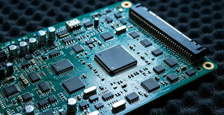
Industrial Machine-Vision Camera PCB Manufacturing: 2026 Process Guide for Step-Height, HDI and mSAP Boards
Industrial AI camera PCBs in 2026 need 12-24 layer HDI/mSAP construction with line widths down to 30µm, controlled stepped-cavity height tolerances of ±25µm, and backdrilled high-speed channels (loss ≤0.012 dB/in @ 10GHz) to hit micron-level vision accuracy without data dropouts.
Shenzhen Hongda Circuit Technology Co., Ltd. (深圳市宏达电路技术有限公司) — Engineering Note, 2026 Process Update
Why Do Industrial AI Vision Camera PCBs Need Micron-Level Precision in 2026?
Because a 1µm sensor-to-lens misalignment on the PCB can translate into a 15-40µm measurement error at the part under inspection, which exceeds the ±10µm tolerance most automotive and semiconductor QC lines demand.
Machine-vision boards are not ordinary digital boards. The image sensor, the lens barrel mount, and the FPC connector all reference the same PCB datum, so any dimensional drift in the board itself is multiplied by the optical magnification ratio of the lens — typically 3x to 8x in industrial inspection setups. On a 25mm sensor PCB, our process data shows that a board with ±50µm flatness deviation across the imaging area produces measurable focus shift at the edges of a 1/1.8″ sensor, which shows up as blurred corners in the captured frame. This is why we control warpage to ≤0.3% per IPC-TM-650 2.4.22 on all camera-class boards, not the ≤0.75% commonly accepted for consumer electronics.
The second driver is data bandwidth. A single 12MP global-shutter sensor running at 60fps generates roughly 5.2 Gbps of raw image data over MIPI CSI-2 or Coax Press lanes. At this speed, dielectric loss and impedance mismatch on the PCB directly degrade signal eye-height, which in turn raises the bit-error rate of the captured frame — not a visible image defect, but a silent data corruption that fails QC algorithms downstream. In 2026, with multi-sensor fusion (RGB + ToF + structured light) becoming standard on inspection stations, boards now carry 3-5 independent high-speed lanes simultaneously, each needing its own controlled-impedance routing and length-matching budget of ≤ ±5 mils.
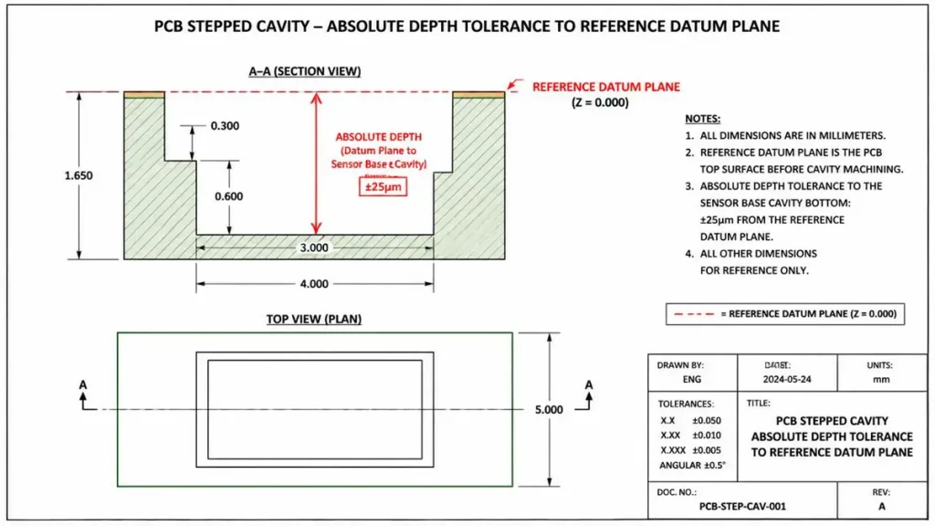
What Step-Height Tolerance Should a Stepped Cavity PCB Hold for Camera Modules?
For machine-vision camera modules with milled sensor cavities or stepped lens-mount pockets, the achievable step-height tolerance is ±25µm on a controlled-depth routing process, and ±50µm on a standard mechanical counterboring process — the difference determines whether autofocus calibration is needed per unit.
Step-height (also called cavity depth or counterbore depth) is the dimension most camera-PCB drawings get wrong, because they specify a target depth without specifying the control method behind it. In our shop, we run three distinct processes depending on tolerance requirement:
| Process | Achievable Step-Height Tolerance | Typical Cavity Depth Range | Best Use Case |
| Controlled-depth CNC routing (depth-sensing spindle) | ±25µm | 0.20mm – 3.0mm | Sensor seating pockets, lens-mount steps |
| Laser-ablated cavity (UV laser, layer-by-layer) | ±15µm | 0.05mm – 0.50mm | Micro-cavities for chip-scale sensor packages |
| Standard mechanical counterboring | ±50µm | 0.20mm – 5.0mm | Connector recesses, non-optical mechanical steps |
| Pre-laminated cavity (selective layer count) | ±one prepreg thickness (≈35µm) | Multiples of 0.1mm layer steps | Multi-depth cavities, stacked sensor boards |
The engineering tradeoff most buyers miss: tightening from ±50µm to ±25µm step-height tolerance adds roughly 12-18% to cavity-machining cost because it requires a dedicated depth-sensing spindle setup and a first-piece CMM (coordinate measuring machine) verification per panel, not per lot. We learned this the hard way on a 2024 automotive lens-mount project: the customer’s drawing called out ±30µm but their fixture only verified flatness, not absolute depth from the reference plane. The result was a batch where step-height was within tolerance individually but the reference datum had shifted 40µm across the panel, causing inconsistent focus across units even though every single measurement “passed.” Since then we require panel-level datum mapping, not single-point measurement, on every stepped-cavity camera PCB order.
Which Layer Stack-Up and HDI Structure Fit High-Resolution Vision Cameras?
Eliminating Hidden Microvia Voids in Any-Layer HDI PCBs via Staggered Layouts
Most 2026-spec industrial vision camera boards use a 12-16 layer Any-Layer HDI stack with 2-3 stacked microvia levels (≥0.1mm/0.1mm line/space) on the sensor-facing side, transitioning to mSAP 30µm lines for the high-speed serializer routing layers.
A typical stack we run for a 12MP global-shutter inspection camera looks like this: Layer 1-2 form a sequential HDI cap (microvia, 0.10mm drill, stacked over a buried via) carrying the sensor’s parallel data and clock lines at controlled 100Ω differential impedance ±10%. Layers 3-6 are mSAP-fabricated signal layers for the MIPI/CoaXPress serializer, where 30µm line width and 30µm space let us route four differential pairs through a 0.4mm pitch BGA without breaking out to an outer layer. The core layers (7-10) carry power distribution with dedicated split planes for the 1.2V sensor core rail and 3.3V I/O rail, isolated by at least 2mm clearance to suppress switching noise into the analog front end.
| Stack Parameter | Specification | Verification Method |
| Total layer count | 12-16L (camera boards), up to 24L for fused multi-sensor heads | Cross-section microscopy, 5 points/panel |
| Outer-layer line/space (mSAP) | 30µm / 30µm, down to 25µm/25µm on request | AOI + SEM sampling per IPC-A-600 Class 3 |
| Microvia diameter | 0.075mm – 0.10mm, aspect ratio ≤0.8:1 | Cross-section, void rate ≤5% |
| Differential impedance (CSI-2/CoaX lanes) | 100Ω ±10%, length-matched ±5 mil pair-to-pair | TDR (time-domain reflectometry) on coupon |
| Dielectric material (high-speed layers) | Df ≤ 0.005 @ 10GHz (low-loss FR-4 or modified-epoxy) | Df/Dk verification per IPC-TM-650 2.5.5.9 |
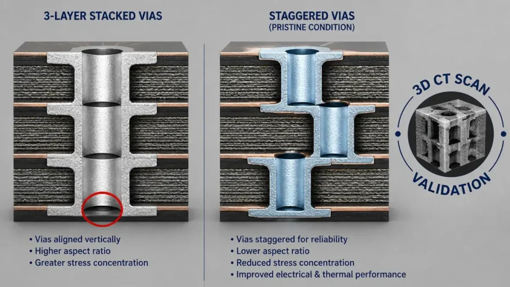
A frequent manufacturing pain point at this stage is microvia void formation when stacking 3 microvia levels directly over each other (stacked, not staggered) on boards thinner than 1.0mm. The thermal mass mismatch during the second and third copper-fill cycles causes incomplete fill at the via base roughly 8-12% of the time on a standard process, which an X-ray inspection alone will not catch because the void sits below resolution at typical 2D X-ray settings. We address this by running 3D CT (computed tomography) scanning on the first article of any stacked-microvia camera board, and by switching to staggered microvias whenever board thickness allows, which cuts the void rate to under 2% in our internal data from the last 18 months of production.
What Are the Real Manufacturing Pain Points for Industrial Vision Camera PCBs?
The four pain points that actually cause field failures are sensor-cavity copper smear during routing, ENIG nickel corrosion under the lens gasket, impedance drift from prepreg resin-flow variation across large panels, and thermal-cycling solder fatigue on the BGA under the image sensor.
Pain point 1: Copper smear inside the sensor cavity
When a cavity is routed through 2-4 layers to seat an image sensor flush against the PCB, the router bit drags a thin smear of copper across the exposed inner-layer pads at the cavity floor. On a standard 2-pass routing program this smear measures 3-8µm thick and is invisible to a 10x optical inspection, but it creates a partial short between adjacent ground and signal pads roughly 1 in 400 cavities in our process baseline. The fix is a dedicated de-smear etch step (plasma or chemical permanganate) specifically inside the cavity after routing, plus a 4-point continuity test on every cavity pad before the sensor is attached — not just a final electrical test, because by then the sensor is already bonded and the board is scrap.
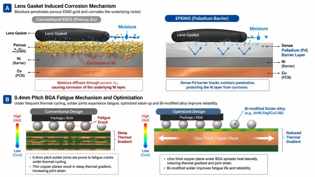
Pain point 2: ENIG corrosion under the lens-mount gasket
Industrial cameras live in environments with coolant mist, dust, and condensation. We have traced three separate field-return cases back to ENIG (electroless nickel immersion gold) surface finish corroding at the lens-mount ground ring, specifically where a rubber gasket trapped moisture against the nickel layer for extended periods. Standard ENIG (gold thickness 0.05-0.1µm, nickel 3-6µm) is porous enough that chloride ions from condensation reach the nickel layer within 400-600 hours of cyclic humidity exposure (per IPC-TM-650 2.6.3 testing we ran internally). For any camera PCB with a sealed gasket interface, we now specify ENEPIG (adding a palladium barrier layer, 0.05-0.15µm) at the gasket contact ring specifically, which extended corrosion onset past 1,500 hours in the same test condition.
Pain point 3: Impedance drift from resin-flow variation
On panels larger than 18″ x 24″, prepreg resin flow during lamination is not perfectly uniform — panels closer to the press platen edge run 0.5-1.0µm thinner dielectric after cure than panels near the center, due to slightly different pressure and heat distribution. On a 100Ω differential pair, this translates to roughly ±3-5Ω impedance variation panel-to-panel, which is within most specs individually but becomes a yield problem when a customer’s high-speed serializer link has a tight ±5Ω budget already consumed by connector and via transitions. Our solution is per-panel TDR sampling (minimum 3 coupons per panel, not 1 per lot) on any board carrying CoaXPress, MIPI, or SLVS-EC interfaces above 2.5 Gbps, with out-of-spec panels segregated before drilling rather than caught at final test.
Pain point 4: Thermal-cycling solder fatigue under the sensor BGA
Image sensors in fixed-position inspection stations cycle through ambient-to-operating temperature swings every time the line starts and stops — in a 3-shift factory this can mean 15-25 thermal cycles per day. Standard SAC305 solder under a 0.4mm-pitch sensor BGA shows measurable fatigue cracking after roughly 3,000-4,000 cycles in our accelerated thermal cycling tests (-40°C to 85°C, IPC-9701 profile), which sounds like years of service but compresses to under a year in high-duty-cycle factory automation. For sensor BGAs specifically, we route a thicker copper plane directly under the BGA footprint (2oz minimum) to spread heat laterally and reduce the local thermal gradient, plus we specify a slightly softer SAC305-with-Bi modified alloy on customer request, which extended cycle life to over 7,000 cycles in the same test in our 2025 qualification data.
How Does PCB Design Change Across Real Industrial Vision Application Scenarios?
Defect-detection cameras on fast-moving lines need backdrilled high-speed lanes for sub-millisecond latency, barcode/logistics cameras need cost-optimized 8-layer boards with relaxed impedance tolerance, and 3D-reconstruction multi-sensor heads need 16-24 layer boards with separated analog/digital grounds for laser-time-of-flight noise isolation.
Scenario A: High-speed defect detection on a production line
A typical line-scan defect-inspection camera running at 200,000 lines/sec to catch surface defects on moving sheet material (steel, glass, film) cannot tolerate signal reflection on its high-speed output lanes, because even a 50-100ps reflection delay shows up as a one-pixel-row timing error that the defect-detection algorithm misreads as a false defect. On these boards we backdrill every via on the CoaXPress or Camera Link HS transmit path to remove the unused via stub below the routing layer, holding stub length under 10 mils (0.25mm). In side-by-side testing on our backdrill line, un-backdrilled stubs of 25-30 mils on a 6 Gbps lane produced eye-diagram closure of 18-22%, while backdrilled stubs under 10 mils kept closure under 5%, directly translating to a measurably lower false-defect rate on the customer’s line.
Scenario B: Warehouse logistics barcode and dimensioning cameras
Logistics scanning cameras (barcode reading, parcel dimensioning) run at much lower data rates — typically under 1 Gbps — and tolerate a wider operating temperature range loosely controlled in a warehouse, so the economic pressure points are different. Here the engineering decision is to drop from a 12-layer HDI build to an 8-layer standard-via build wherever the design allows, which in our cost modeling reduces board fabrication cost by roughly 35-45% without a measurable impact on read-rate accuracy, since the bottleneck for barcode decode speed is almost always the sensor and optics, not the PCB signal integrity margin at sub-1Gbps rates.
Scenario C: 3D reconstruction with fused ToF, structured light, and RGB sensors
Multi-modal 3D reconstruction heads (combining a Time-of-Flight depth sensor, a structured-light projector driver, and an RGB image sensor on one PCB) face a specific noise problem: the ToF sensor’s laser driver switches current at 10-20MHz with switching edges that radiate broadband noise directly into the adjacent RGB sensor’s analog front end if the two are not properly separated. Our solution on these boards is a split-ground design — physically separate analog and digital ground planes connected only through a single star-point near the connector — combined with a guard-ring of stitching vias (spaced ≤2mm) around the laser driver section. In a 2025 qualification project for a warehouse robotics customer, this design reduced measured RGB sensor noise floor by approximately 6dB compared to the customer’s previous single-ground-plane design, which directly improved low-light image quality used for object recognition.
What Testing and Reliability Standards Apply to Industrial Camera PCBs in 2026?
Industrial vision camera boards in 2026 are typically qualified to IPC-6012 Class 3 (or 3/A for harsh environments), IPC-TM-650 2.4.22 warpage ≤0.3%, AOI + 3D CT scanning on stacked microvias, and a minimum 1,000-hour humidity/thermal-cycling reliability test before release to mass production.
Beyond standard electrical test (flying probe or bed-of-nails at 100% coverage), camera-class boards in our 2026 process flow add three inspection gates that general digital boards skip: a dedicated cavity-floor continuity check after routing (catching the copper-smear issue above before sensor attach), 3D CT sampling on stacked-microvia regions at a minimum 1 panel per lot, and a panel-level flatness map (not single-point) recorded against the IPC-TM-650 2.4.22 ≤0.3% warpage limit, because flatness measured at the panel center can pass while the imaging area at the panel edge fails.
| Test | Standard / Method | Acceptance Criterion |
| Warpage / flatness | IPC-TM-650 2.4.22, panel-mapped | ≤0.3% over imaging area |
| Microvia void inspection | 3D CT (computed tomography) | Void rate ≤2% per via, no voids >25% of via volume |
| Impedance verification | TDR, 3 coupons/panel minimum | 100Ω ±10%, pair skew ≤5 mil |
| Thermal cycling | IPC-9701, -40°C to 85°C | Pass 1,000 cycles, no BGA crack >25% of joint |
| Humidity / corrosion (ENEPIG) | IPC-TM-650 2.6.3, 85°C/85%RH | No visible corrosion at 1,500 hours |
How Should Buyers Specify Step-Height and Tolerance Requirements on a PCB Drawing?
Specify step-height with a clear reference datum (not just a target depth), state the verification method required (panel-mapped CMM vs. single-point), and separate the optical-critical cavity tolerance from non-optical mechanical steps so the fab does not apply the same ±50µm default to a feature that actually needs ±25µm.
Most quotation delays we see on camera-PCB RFQs come from an incomplete cavity callout. A drawing that says “cavity depth 0.5mm ±0.05mm” without specifying the reference plane leaves the fab guessing whether that’s measured from the top copper, the board’s nominal finished thickness, or the bottom of the cavity relative to the opposite surface — each interpretation can differ by 30-60µm on a multilayer board with normal lamination press-fit tolerance. Our DFM checklist for new camera-board customers always asks for: (1) the exact reference surface for the depth dimension, (2) whether the tolerance is for an individual cavity or must hold true across the full panel (datum consistency), and (3) which cavities are optically critical (need ±25µm + panel-mapped CMM) versus purely mechanical (the standard ±50µm counterboring tolerance is fine and cheaper).
Summary: Turning 2026 Process Capability Into a Reliable Camera PCB
Industrial AI vision camera PCBs in 2026 succeed or fail on details that don’t show up in a basic spec sheet: which step-height process actually holds ±25µm versus ±50µm, whether microvias are staggered or stacked, whether ENIG or ENEPIG survives the gasket environment, and whether impedance was verified per-panel or per-lot. At Shenzhen Hongda Circuit Technology Co., Ltd., these are the exact checkpoints we run on every industrial vision camera PCB order, from DFM review through 3D CT inspection and thermal-cycling qualification.
For DFM review, prototype runs, or volume production of HDI/mSAP industrial camera PCBs, our engineering team can walk through your cavity datum, stack-up, and impedance budget before quotation.
FAQ
What step-height tolerance can a PCB factory hold for a camera sensor cavity?
A controlled-depth CNC routing process holds ±25µm; standard mechanical counterboring holds ±50µm; laser-ablated micro-cavities can hold ±15µm for very shallow depths under 0.5mm.
How many layers does a typical industrial vision camera PCB use in 2026?
Most single-sensor inspection cameras use 12-16 layer Any-Layer HDI stacks; multi-sensor fusion heads (RGB + ToF + structured light) commonly go to 16-24 layers to separate analog and digital grounds.
Why does backdrilling matter for machine-vision camera PCBs?
Backdrilling removes the unused via stub on high-speed transmit lanes; un-backdrilled stubs over 25 mils caused 18-22% eye-diagram closure in internal testing at 6 Gbps, while stubs under 10 mils kept closure under 5%.
Is ENIG or ENEPIG better for camera PCBs with a sealed lens gasket?
ENEPIG is preferred at the gasket contact ring because its palladium barrier layer delayed corrosion onset to over 1,500 hours in 85°C/85%RH testing, versus 400-600 hours for standard ENIG in the same condition.
What causes false defect detections on high-speed line-scan camera PCBs?
Signal reflection from un-backdrilled via stubs or impedance mismatch can create timing errors as small as 50-100ps, which a line-scan defect algorithm can misread as a one-pixel-row false defect.
How is microvia void rate controlled on stacked-microvia camera boards?
3D CT (computed tomography) scanning on the first article catches sub-surface voids that 2D X-ray misses; switching from stacked to staggered microvias where board thickness allows reduced void rate from 8-12% to under 2% in internal data.
Find Out About Us: Delivering Top-Tier Fabrication for Both AI & Conventional PCBs
Navigating the line between cutting-edge innovation and high-volume, cost-effective production shouldn’t be a compromise. At Shenzhen Hongda Circuit Technology (PCBKR), we bridge this gap by elevating the manufacturing standards for both high-performance AI hardware and traditional multi-layer PCBs.
By integrating advanced manufacturing methodologies across all production lines, we bring an elite level of precision to traditional PCB fabrication. Our standard boards benefit from enhanced interlayer alignment tolerances (down from ±75μm to within ±25μm) and tightened differential impedance control (±5%). Supported by 100% 3D X-Ray (AXI) inspection, your conventional boards achieve chip-level reliability, superb signal stability, and near-100% yield.
Your Strategic Manufacturing Partner
We proudly stand as a dual-capability partner: offering the elite technical ceiling required for next-gen AI hardware, while maintaining the exceptional flexibility, rapid turnaround, and unmatched cost-efficiency needed for mid-to-high-volume traditional board campaigns. You get zero-defect reliability without the premium overhead or bureaucracy of massive tier-1 factories.
Ready to upgrade your hardware’s reliability?
Submit your Gerber files today for an agile engineering review and a highly competitive quote.
Contact our experts: sales@pcbkr.com
About Author
David Chen https://www.linkedin.com/in/pcbcoming
David Chen boasts an extensive professional background in PCBA manufacturing, PCBA testing, and PCBA optimization, with specialized expertise in high-precision PCBA fault analysis and rigorous PCBA reliability testing. The author has worked with high-layer-count server PCB fabrication, ultra-low-loss backplane stackups, and thermo-mechanical reliability optimization for AI infrastructure projects involving 112G and 224G PAM4 architectures. Skilled in complex circuit design and cutting-edge advanced PCB manufacturing processes, he delivers solutions that elevate product durability and performance across industrial applications. His technical articles focusing on PCBA manufacturing workflows and testing methodologies are widely cited by industry peers, research institutions, and technical platforms, solidifying his reputation as a recognized technical authority in the global circuit board manufacturing sector.