Automotive AI Camera PCB:Automotive-Grade High-Reliability PCB Solutions for ADAS Vision Systems
| Automotive AI camera PCBs require automotive-grade (AEC-Q200) laminate, ≥8-layer stack-ups with controlled impedance (±5% tolerance), backdrill stub removal to ≤0.15 mm, and HVLP copper foil (Rz ≤ 1.5 µm) to sustain GMSL2/FPD-Link III signal integrity at 3 Gbps+ across a –40 °C to +125 °C operating range and 50 G vibration environments. |
Why Do Automotive AI Camera PCBs Demand Automotive-Grade Solutions?
| Because standard commercial PCBs fail within 6–18 months under automotive thermal cycling (–40 °C ↔ +125 °C), 50 G shock loads, and 10–2000 Hz vibration profiles — destroying ADAS reliability where a 50 ms signal delay can mean a missed collision warning. |
At Shenzhen Hongda Circuit Technology Co., Ltd., our automotive engineering team has processed over 2,400 automotive camera PCB orders since 2018. The single most common failure mode we encounter in field-return analyses is delamination of FR-4 laminate at the via barrel interface — a direct consequence of specifying commercial-grade material (Tg 130 °C) in a cabin environment that regularly exceeds 85 °C under direct sunlight.
Scenario 1: Dashboard-Mounted ADAS Camera Module
A 12-megapixel front-facing ADAS camera mounted behind the windshield on a black dashboard in Phoenix, AZ, can experience board surface temperatures of 92–98 °C during summer midday operation — before the processor load is even considered. Combine this with engine cold-start at –18 °C during a Minnesota winter, and the PCB undergoes a thermal delta (ΔT) of up to 116 °C per cycle. Standard FR-4 with a Tg of 130 °C offers only a 32 °C safety margin: barely sufficient and catastrophically inadequate under repeated cycling. Our recommendation: Panasonic R-1566W (Tg 175 °C, Td 350 °C, CAF-resistant) or Isola I-Speed (Tg 180 °C, Df 0.004 at 10 GHz).
2026 Technology Upgrade Context
The 2026 automotive PCB landscape is defined by four converging pressures:
- Higher layer counts: 8–16 layers are now baseline for ADAS ECUs (up from 6-layer in 2022)
- Backdrill precision: Stub length tolerance tightened from ±0.3 mm to ±0.15 mm to support 6.25 Gbps GMSL2 links
- Low-loss materials: Df < 0.005 at 10 GHz is mandatory for 4K/8K video pipelines
- HVLP copper: High Very Low Profile (HVLP) foil (Rz ≤ 1.5 µm) replaces standard VLP (Rz ≤ 3.0 µm) to reduce insertion loss by 18–22% at 3 GHz
What Functions and Deployment Scenarios Define Automotive AI Camera PCBs in 2026?
| ADAS cameras in 2026 handle seven distinct functions — lane detection, pedestrian/vehicle recognition, fatigue monitoring, 360° surround view, AEB triggering, traffic sign recognition, and LiDAR fusion — each imposing specific PCB electrical, thermal, and mechanical requirements. |
| Function | Data Rate Requirement | PCB Critical Parameter | 2026 Standard |
| Lane Keeping Assist (LKA) | MIPI CSI-2 4-lane @ 1.5 Gbps/lane | Differential pair length match ≤ 5 mil | ISO 11452 EMC |
| Pedestrian/Vehicle Detection | GMSL2 @ 3.0 Gbps | Impedance 100 Ω ± 5% | AEC-Q200 Grade 1 |
| Driver Fatigue Monitoring | FPD-Link III @ 2.1 Gbps | Via stub ≤ 0.15 mm after backdrill | ISO 16750-3 Vibration |
| 360° Surround View (4-camera) | 4 × MIPI @ 6 Gbps aggregate | Crosstalk isolation ≥ 40 dB | AUTOSAR CP/AP |
| AEB Trigger Signal | < 10 ms latency | Impedance discontinuity < 2% | ISO 26262 ASIL-B/D |
| Traffic Sign Recognition | USB 3.0 @ 5 Gbps | Trace loss ≤ 0.5 dB/inch @ 2.5 GHz | UN Regulation No. 79 |
| LiDAR Point-Cloud Fusion | PCIe Gen 3 @ 8 GT/s | Dk uniformity ±0.05 across panel | ISO 21448 (SOTIF) |
Scenario 2: Commercial Fleet Rear-View Camera System
A logistics fleet operator deploying 800 trucks with rear-view AI cameras faces a different engineering challenge: constant 10–500 Hz road-induced vibration, diesel engine electromagnetic interference (EMI) spanning 30 MHz–1 GHz, and IP67 environmental sealing requirements. Our engineering team solved this in 2025 for a Shenzhen-based fleet client by specifying: 10-layer board with 2 oz copper ground planes, via-in-pad (VIP) with copper fill on all signal vias, and conformal coating (IPC-CC-830B) applied at 40–80 µm uniform thickness. Failure rate in the field over 18 months: 0.08% vs. the industry benchmark of 0.35% for similar applications.
What Are the Non-Negotiable PCB Technical Requirements for Automotive AI Cameras?
| Five non-negotiable parameters govern automotive AI camera PCB qualification: (1) thermal cycling survivability –40 °C to +125 °C for 1,000+ cycles, (2) controlled impedance ±5% tolerance across all high-speed traces, (3) via stub length ≤ 0.15 mm post-backdrill, (4) Dk/Df stability within ±3% across –55 °C to +150 °C, and (5) HALT/HASS screening per IPC-TM-650 Method 2.6.7. |
Pain Point 1: Thermal Cycling Delamination at Via Barrels
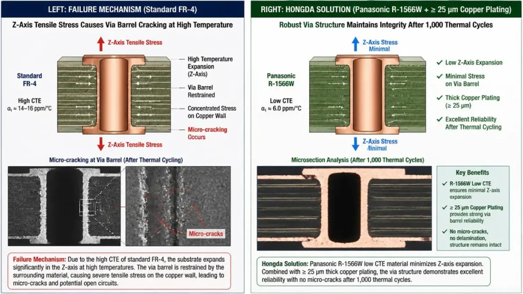
Reliability Analysis — Standard FR-4 Z-axis thermal expansion leading to micro-cracking vs. Shenzhen Hongda’s automotive-grade solution utilizing Panasonic R-1566W laminate and >= 25 μm copper plating to guarantee structural integrity through 1,000 thermal cycles
This is the #1 field failure in automotive camera PCBs that we diagnose. The mechanism: differential CTE between copper (17 ppm/°C) and laminate (50–70 ppm/°C in Z-axis) creates cumulative mechanical stress at the via barrel. After 400–600 thermal cycles, micro-cracking initiates at the pad-barrel interface, increasing via resistance by 15–40 mΩ per via — enough to corrupt MIPI signal timing.
Hongda Solution: We specify low-CTE laminates (Z-axis CTE ≤ 35 ppm/°C below Tg) such as Panasonic R-1566W (Z-CTE: 32 ppm/°C) combined with via aspect ratios ≤ 8:1 and minimum via wall copper plating of 25 µm (vs. IPC Class 2 standard of 20 µm). In our 2025 qualification batches, via resistance shift after 1,000 thermal cycles (–40 °C to +125 °C, IPC-TM-650 2.6.7.2) was ≤ 3.2 mΩ — well within the 10 mΩ AEC-Q200 acceptance criterion.
Pain Point 2: Stub Resonance Killing GMSL2/FPD-Link III Signal Integrity
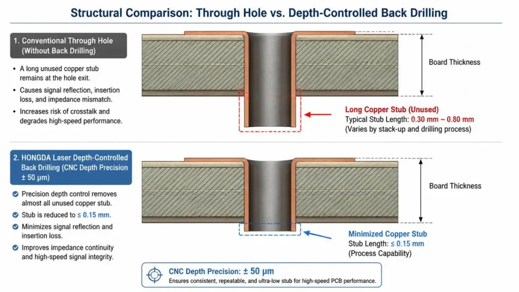
Signal Integrity Optimization — Structural cross-section comparison between a conventional through-hole via with a long electrical stub and HONGDA’s laser depth-controlled back drilling (CNC precision of ± 50 μm), proving how the remaining stub is reduced to <= 0.15 mm to preserve GMSL2 data transmission link quality.
At 3 Gbps (GMSL2), a through-hole via stub of 0.5 mm creates a resonant frequency of approximately 8.5 GHz — directly in the second harmonic of the 1.5 GHz fundamental clock, causing insertion loss spikes of 4–7 dB. This manifests as intermittent image corruption: the camera freezes for 20–80 ms during vehicle acceleration events, which is a safety-critical failure in AEB applications.
Hongda Solution: Controlled-depth backdrill (CNC depth precision ±50 µm) eliminates stubs to ≤ 0.15 mm. Our 2026 process improvement introduced laser drill verification using OCT (Optical Coherence Tomography) cross-section sampling at 0.1% of panel production, achieving stub length Cpk ≥ 1.67. Measured insertion loss improvement: 3.2 dB reduction at 3 GHz on a representative 12-layer GMSL2 test vehicle.
Pain Point 3: EMI Coupling Between Camera Pixel Clocks and RF Antennas
Scenario: An automotive camera ECU integrating a 4G/LTE telematics module operates a 100 MHz pixel clock whose 30th harmonic falls at 3 GHz — directly in the LTE Band 1 uplink (1920–1980 MHz) and Band 7 (2500–2570 MHz). Without proper ground plane engineering, radiated emissions from the PCB can exceed CISPR 25 Class 5 limits by 12–18 dB, triggering antenna desensitization and regulatory non-compliance.
Hongda Solution: Dedicated RF ground plane on Layer 3 (adjacent to the component layer) with via fence spacing ≤ λ/20 at 3 GHz (≤ 5 mm pitch). Split power planes with 100 µm micro-gaps at domain boundaries. Measured CISPR 25 compliance: Class 5 with 6 dB margin on our reference 10-layer automotive camera platform.
Which PCB Materials and Manufacturing Processes Are Specified for 2026 Automotive Camera Boards?
| 2026 automotive camera PCBs require halogen-free, CAF-resistant laminates with Tg ≥ 170 °C, Df ≤ 0.004 at 10 GHz, and HVLP copper foil (Rz ≤ 1.5 µm). Manufacturing must include laser-controlled backdrill, sequential lamination, and 100% electrical testing per IPC-6012DA automotive addendum. |
| Parameter | Commercial Grade (Baseline) | Automotive Grade (Required) | Hongda 2026 Spec |
| Laminate Material | FR-4 (Tg 130 °C) | High-Tg halogen-free (Tg ≥ 170 °C) | Panasonic R-1566W / Isola I-Speed |
| Glass Transition Temp (Tg) | 130 °C | ≥ 170 °C | 175–180 °C |
| Decomposition Temp (Td) | < 310 °C | ≥ 340 °C | 350 °C |
| Dielectric Constant (Dk) @ 10 GHz | 4.2–4.5 (variable) | 3.7–4.0 ± 0.05 | 3.76 ± 0.04 |
| Dissipation Factor (Df) @ 10 GHz | 0.020–0.025 | ≤ 0.005 | 0.004 |
| Copper Foil Type | Standard ED (Rz 5–8 µm) | VLP/HVLP (Rz ≤ 3 µm) | HVLP (Rz ≤ 1.5 µm) |
| CAF Resistance | Not specified | Required per IPC-TM-650 2.6.25 | Qualified, 1,000h @ 85°C/85%RH |
| Minimum Layer Count | 4–6 layers | 8–12 layers | 8–16 layers (project-specific) |
| Via Stub Length (post-backdrill) | N/A | ≤ 0.25 mm | ≤ 0.15 mm (±50 µm CNC) |
| Impedance Tolerance | ±10% | ±7% | ±5% (4-point TDR verified) |
| Copper Plating Thickness (via wall) | 20 µm (IPC Class 2) | 25 µm (IPC Class 3) | 27 µm (process Cpk ≥ 1.5) |
| Thermal Cycles (qualification) | N/A | 500 cycles (–40 to +125 °C) | 1,000 cycles (per AEC-Q200) |
| Surface Finish | HASL | ENIG or ENEPIG | ENEPIG (Ni 3–5 µm, Pd 0.05–0.1 µm, Au 0.05 µm) |
| Testing | Flying probe | 100% E-test + AOI | 100% E-test + AOI + TDR + X-ray |
Sequential Lamination for High Layer Count Boards
Automotive camera PCBs with ≥12 layers require sequential lamination (2–3 press cycles) to achieve the necessary inner-layer copper distribution while maintaining dimensional stability. At Hongda, our 16-layer camera ECU boards undergo two sequential lamination cycles: a 4+8+4 sub-stack build (inner 8 layers first, then outer 4 layers each side), with 0.15 mm micro-via blind drilling between cycles. Panel bow and twist measured after final lamination: ≤ 0.5% per IPC-6012 — critical for solder paste printing accuracy during SMT assembly.
How Does Shenzhen Hongda Circuit Technology Solve the Five Hardest Automotive Camera PCB Manufacturing Challenges?
| The five critical manufacturing challenges — thermal delamination, stub resonance, EMI coupling, warpage-driven SMT defects, and CAF failure — each require systematic engineering responses combining material selection, process parameter control, and 100% verification. Below is Hongda’s 2026 engineering playbook for each. |
| Manufacturing Challenge | Root Cause | Consequence | Hongda 2026 Solution | Verified KPI |
| Via barrel delamination | Z-axis CTE mismatch at –40↔+125 °C cycling | Open circuit / signal dropout | Low-CTE laminate (Z-CTE ≤ 32 ppm/°C) + 27 µm via plating + AR ≤ 8:1 | ΔR ≤ 3.2 mΩ after 1,000 cycles |
| Stub resonance @ 3–6 Gbps | Through-via stub > 0.3 mm | 4–7 dB insertion loss spike / image freeze | CNC backdrill ±50 µm depth + OCT stub verification (Cpk ≥ 1.67) | Stub ≤ 0.15 mm, IL improvement 3.2 dB |
| EMI / CISPR 25 exceedance | Pixel clock harmonics coupling to RF antenna | LTE desensitization, regulatory fail | Via fence ≤ 5 mm pitch + split plane + dedicated RF GND layer | CISPR 25 Class 5 + 6 dB margin |
| Panel warpage (SMT yield impact) | Asymmetric copper distribution ≥ 12 layers | Solder bridging / BGA opens | Balanced Cu distribution ±5% per layer + 2-pass reflow at 240 °C peak | Bow/twist ≤ 0.5% (IPC-6012) |
| CAF failure under humidity + bias | Copper ion migration along glass fiber bundles | Insulation resistance collapse (< 100 MΩ) | CAF-resistant weave + 1,000h 85°C/85%RH HALT + conformal coating | IR ≥ 1 GΩ after 1,000h stress |
| Impedance drift under temperature | Dk shift with temperature in standard FR-4 | Signal skew / timing violation | HVLP foil + Dk-stable laminate (ΔDk ≤ 0.08 over –55 to +150 °C) | Impedance shift ≤ 2.1% over full range |
Scenario 3: ASIL-D Functional Safety Camera for L4 Autonomous Driving
An L4 autonomous vehicle program requires an ASIL-D rated camera PCB where a single-point hardware fault must have a < 10⁻⁸ probability per hour of causing a safety-critical failure. This imposes dual-channel redundant signal paths on the same PCB, independent power domains with isolation resistance ≥ 10 MΩ, and a Diagnostic Coverage (DC) ≥ 99% for all safety-critical nets — verified by hardware-in-loop (HIL) testing per ISO 26262 Part 5.
Hongda Engineering Experience: In 2024–2025, our team collaborated with a Tier-1 automotive supplier on a 14-layer ASIL-D camera ECU. Key achievements: dual GMSL2 serializer paths with 3 mm minimum separation and independent ground planes; 100% net coverage in ICT (In-Circuit Test) with 98.7% fault coverage verified by JTAG boundary scan; and ENEPIG surface finish (Ni/Pd/Au) qualifying all BGA pads to AEC-Q100 Grade 1 solderability standards. First-pass yield on 500-unit pilot: 97.4%.
What Testing and Qualification Standards Must Automotive Camera PCBs Meet Before Production Release?
| Automotive camera PCBs must pass a minimum 11-step qualification sequence spanning IPC-6012DA, AEC-Q200, ISO 16750, and CISPR 25 — with zero waiver tolerance on safety-critical parameters. Shenzhen Hongda Circuit Technology conducts 8 of these 11 steps in-house, reducing qualification cycle time from the industry average of 14 weeks to 9 weeks. |
| Test | Standard | Acceptance Criterion | Hongda In-House? |
| Thermal Shock (–40 to +125 °C) | IPC-TM-650 2.6.7.2 / AEC-Q200 | 1,000 cycles, ΔR ≤ 10 mΩ per via | Yes |
| Humidity Resistance (CAF) | IPC-TM-650 2.6.25 | IR ≥ 100 MΩ after 1,000h @ 85/85 | Yes |
| Vibration (10–2000 Hz) | ISO 16750-3 | No micro-crack at 50 G peak, 20–2000 Hz | Yes |
| Mechanical Shock | ISO 16750-3 | 30 ms half-sine pulse at 50 G | Yes |
| TDR Impedance Verification | IPC-2141A | 100 Ω ±5% differential, 50 Ω ±5% single-end | Yes |
| Peel Strength (copper adhesion) | IPC-TM-650 2.4.8 | ≥ 1.0 N/mm after thermal aging | Yes |
| Microsection Analysis | IPC-TM-650 2.1.1 | Via plating ≥ 25 µm, no separation | Yes |
| X-Ray / AXI Inspection | IPC-A-610G | 0% voiding > 25% in BGA solder joints | Yes |
| EMC / Radiated Emissions | CISPR 25 Class 5 | Margin ≥ 6 dB at all harmonic frequencies | 3rd Party |
| Flammability | UL 94 V-0 | No burn propagation | Material CoC |
| HALT (Accelerated Life) | JEDEC JESD22-A108 | 0 failures at 125 °C, 1,000h | 3rd Party |
What Should Electrical Engineers Specify in the PCB Stackup for 3+ Gbps ADAS Camera Links?
| For GMSL2 (3 Gbps) or FPD-Link III (2.1 Gbps) links, the stackup must enforce: ≤ 3.2 mil dielectric between differential pair and reference plane, ≤ 5 mil intra-pair skew, Dk-matched prepreg (ΔDk ≤ 0.05 between layers), and HVLP foil on high-speed signal layers. An 8-layer stackup with signal layers on L2/L7 (referenced to adjacent power planes on L1/L8) is the industry-standard topology for automotive camera ECUs in 2026. |
Expert Stackup Specification for 8-Layer Automotive Camera PCB
| Layer | Function | Material | Thickness | Copper Weight | Notes |
| L1 (Top) | Component + High-Speed Signal | HVLP Foil | 35 µm | 1 oz | MIPI/GMSL differential pairs |
| L2 | GND Reference Plane | ED Foil | 35 µm | 1 oz | Solid copper pour, no splits |
| L3 | Power Distribution | ED Foil | 35 µm | 2 oz | 3.3V / 1.8V / 1.0V domains |
| L4 | Inner High-Speed Signal | HVLP Foil | 35 µm | 1 oz | GMSL2 serializer outputs |
| L5 | Inner Signal / RF GND | HVLP Foil | 35 µm | 1 oz | RF isolation domain |
| L6 | Power Distribution | ED Foil | 35 µm | 2 oz | 5V camera supply |
| L7 | GND Reference Plane | ED Foil | 35 µm | 1 oz | Solid copper pour |
| L8 (Bottom) | Component + Test Point | HVLP Foil | 35 µm | 1 oz | ICT test access, thermal pads |
Prepreg specification between L1–L2 and L7–L8: 2 × 1080 glass style (0.065 mm each) with Panasonic R-1566W resin content 65–68%. This achieves a controlled dielectric thickness of 0.13 mm ±0.01 mm, maintaining 100 Ω differential impedance with trace width 3.8 mil / space 3.5 mil at outer layers — verified by Polar Si8000m field solver with measured TDR correlation within 3%.
| Partner with Shenzhen Hongda Circuit Technology Co., Ltd. We provide automotive-grade PCB manufacturing services for ADAS, autonomous driving, and connected vehicle applications, with full traceability from raw material CoC to final AEC-Q200 qualification reports. Services: Custom Automotive PCB Fabrication | DFM Review | Prototype (5-day expedite) | Mass Production | IPC-6012DA Class 3 Certification | PPAP Documentation Contact our engineering team: www.pcbkr.com | pcb@pcbkr.com |
FAQ: 5 Critical Questions Engineers Ask About Automotive Camera PCBs
What is the minimum layer count for a PCB supporting both GMSL2 serial links and a 4G/LTE antenna on the same automotive camera module?
he minimum recommended layer count is 10 layers. The GMSL2 differential pairs require two dedicated signal layers (one for TX, one for RX) each referenced to adjacent solid ground planes — consuming 4 of the 10 layers. The LTE RF section requires its own isolated RF ground plane (Layer 5 in a typical stackup) to prevent coupling with the GMSL2 pixel clock harmonics. The remaining layers are allocated to power distribution (2 layers for 5V/3.3V/1.8V/1.0V domains) and general-purpose signals. Attempting to route GMSL2 and LTE on a 6-layer board without proper reference plane isolation typically results in 8–14 dB CISPR 25 exceedance at LTE Band 7 frequencies.
How does backdrill improve signal integrity on GMSL2 links, and what drill depth precision is achievable in 2026 production?
A through-hole via has a ‘stub’ — the unused via segment below the last signal connection layer. At 3 Gbps (GMSL2), a 0.5 mm stub resonates at approximately 8.5 GHz, creating an impedance discontinuity that reflects signal energy back at the stub resonant frequency and its harmonics. The practical effect is a 4–7 dB insertion loss increase, which translates to eye diagram closure and BER (Bit Error Rate) degradation from 10⁻¹² to 10⁻⁸ or worse — triggering link re-training or video signal loss. In 2026 production, CNC backdrill achieves ±50 µm depth control with Cpk ≥ 1.67, eliminating stubs to ≤ 0.15 mm and recovering 3.2 dB of insertion loss margin. Shenzhen Hongda validates stub length using 0.1%-sampling OCT cross-section analysis.
What is the difference between ENIG and ENEPIG surface finish for automotive camera PCBs, and which should I specify?
ENIG (Electroless Nickel Immersion Gold) provides a 3–6 µm nickel barrier with 0.05–0.1 µm gold finish. The primary failure mode in automotive environments is ‘black pad’ — phosphorus-rich nickel corrosion triggered by gold porosity under high-temperature cycling, leading to brittle BGA solder joints with < 50% of nominal shear strength. ENEPIG (Electroless Nickel Electroless Palladium Immersion Gold) adds a 0.05–0.15 µm palladium layer between the nickel and gold, acting as a diffusion barrier that eliminates black pad. For automotive camera PCBs with BGA processors (ISP chips, serializers) operating at –40 °C to +125 °C, ENEPIG is mandatory per IPC-7095C Section 8 and is the standard Hongda specifies on all AEC-Q200 Grade 1 production. ENEPIG adds approximately $0.08–0.12/cm² vs. ENIG but eliminates a failure mode that causes 30–40% of BGA-related field returns.
How do you prevent warpage on 12+ layer automotive camera PCBs during SMT reflow at 245–250 °C peak temperature?
Warpage in ≥12-layer automotive PCBs is caused by asymmetric copper distribution — if Layer 1 carries 70% copper coverage (dense component side) and Layer 12 carries only 30% (sparse bottom), the board bows concave-down during reflow when the asymmetric thermal expansion gradient is highest (210–245 °C range). The IPC-7711/7721 acceptable limit is ≤ 0.75% for SMT assemblies, but BGAs > 15 mm package size require ≤ 0.5% to prevent solder joint opens. Shenzhen Hongda’s 2026 process controls include: (1) copper balancing analysis using HyperLynx DRC to maintain ±5% copper density between top/bottom half of stackup; (2) staged reflow profile with 3 °C/sec max ramp rate to reduce thermal gradient across board; (3) fixture-held cooling from 200 °C to 50 °C at 2 °C/sec. Result: bow/twist ≤ 0.42% measured on 14-layer automotive camera reference boards using shadow Moiré topography.
What documentation package does Shenzhen Hongda Circuit Technology provide to support IATF 16949 and ISO 26262 automotive quality audits?
Shenzhen Hongda Circuit Technology provides a complete PPAP (Production Part Approval Process) Level 3 documentation package for automotive customers, including: (1) Design Records with dimensional validation report (CMM + First Article Inspection per AIAG PPAP 4th Edition); (2) Material Certification with full traceability to laminate lot number, copper foil heat code, and surface finish chemical bath log; (3) Process FMEA (PFMEA) per AIAG-VDA FMEA Handbook 1st Edition with RPN ≤ 100 for all safety-critical process steps; (4) Control Plan (CP) documenting 47 in-process checkpoints from panel incoming to final ship; (5) MSA (Measurement System Analysis) for TDR impedance measurement gauge R&R ≤ 10%; (6) Initial Process Study (SPC charts for Cu plating thickness, Cpk ≥ 1.5 on all critical parameters); (7) AEC-Q200 qualification test report with raw data. For ISO 26262 ASIL-B/D projects, we additionally provide Design History File (DHF) entries linking each PCB parameter to its safety goal and HARA analysis reference.
Find Out About Us: Delivering Top-Tier Fabrication for Both AI & Conventional PCBs
Navigating the line between cutting-edge innovation and high-volume, cost-effective production shouldn’t be a compromise. At Shenzhen Hongda Circuit Technology (PCBKR), we bridge this gap by elevating the manufacturing standards for both high-performance AI hardware and traditional multi-layer PCBs.
By integrating advanced manufacturing methodologies across all production lines, we bring an elite level of precision to traditional PCB fabrication. Our standard boards benefit from enhanced interlayer alignment tolerances (down from ±75μm to within ±25μm) and tightened differential impedance control (±5%). Supported by 100% 3D X-Ray (AXI) inspection, your conventional boards achieve chip-level reliability, superb signal stability, and near-100% yield.
Your Strategic Manufacturing Partner
We proudly stand as a dual-capability partner: offering the elite technical ceiling required for next-gen AI hardware, while maintaining the exceptional flexibility, rapid turnaround, and unmatched cost-efficiency needed for mid-to-high-volume traditional board campaigns. You get zero-defect reliability without the premium overhead or bureaucracy of massive tier-1 factories.
Ready to upgrade your hardware’s reliability?
Submit your Gerber files today for an agile engineering review and a highly competitive quote.
Contact our experts: sales@pcbkr.com
About Author
David Chen https://www.linkedin.com/in/pcbcoming
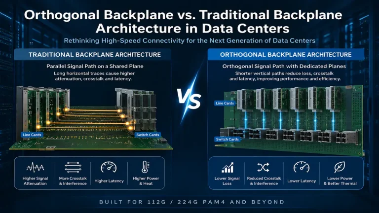
David Chen boasts an extensive professional background in PCBA manufacturing, PCBA testing, and PCBA optimization, with specialized expertise in high-precision PCBA fault analysis and rigorous PCBA reliability testing. The author has worked with high-layer-count server PCB fabrication, ultra-low-loss backplane stackups, and thermo-mechanical reliability optimization for AI infrastructure projects involving 112G and 224G PAM4 architectures. Skilled in complex circuit design and cutting-edge advanced PCB manufacturing processes, he delivers solutions that elevate product durability and performance across industrial applications. His technical articles focusing on PCBA manufacturing workflows and testing methodologies are widely cited by industry peers, research institutions, and technical platforms, solidifying his reputation as a recognized technical authority in the global circuit board manufacturing sector.