How to Audit & Qualify a Controlled Impedance PCB Manufacturer for 112G/224G Applications
In the era of 112G/224G PAM4 signaling and AI server infrastructure, selecting the wrong controlled impedance PCB manufacturer doesn’t just lead to signal integrity (SI) failures—it triggers costly respins, delayed time-to-market, and supply chain disruptions that can derail entire product launches.
If you’re a procurement or hardware engineering leader sourcing high-speed PCBs, you’ve likely encountered this frustrating scenario: the sample panels pass TDR testing with flying colors, but batch production yields boards with impedance drift that causes system-level compliance failures. The root cause? Most teams evaluate manufacturers based on static datasheets rather than statistical process control.
This guide dismantles that approach. Below, you’ll find a comprehensive framework for evaluating, auditing, and selecting a controlled impedance PCB manufacturer with genuine high-precision capability—covering engineering competence, equipment benchmarks, and a field-ready audit checklist.
1. The Blind Spots of Traditional Evaluation: Why You Can’t Rely on Datasheets Alone
Marketing brochures promise the world. Here’s what they typically leave out.
Blind Spot #1: Static Tolerance vs. Statistical Process Control
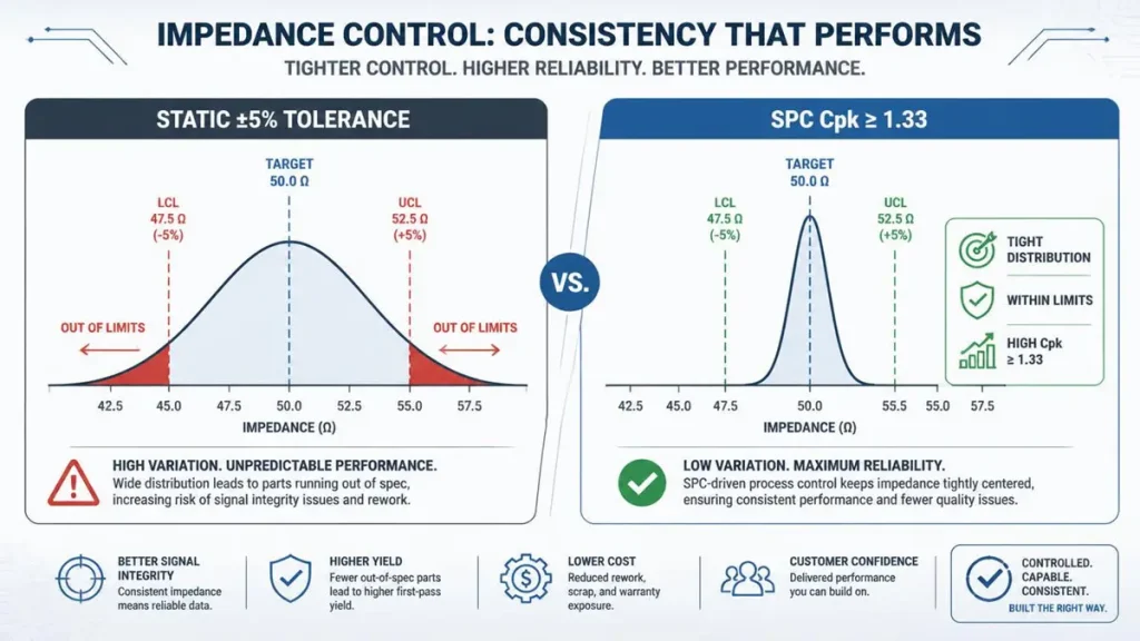
Static ±5% Impedance Tolerance vs. SPC Cpk ≥ 1.33 Comparison
A manufacturer claiming ±5% impedance tolerance is not the same as one that reliably achieves it across thousands of panels. Static tolerance is a single-point measurement; process capability is a statistical reality.
What to demand: A qualified controlled impedance PCB manufacturer must provide real-time SPC data demonstrating Cpk ≥ 1.33 for critical impedance traces. Cpk (process capability index) measures how consistently a process stays within specification limits. Without it, you’re buying a lottery ticket, not a manufacturing process.
Red flag: If a factory cannot produce Cpk trend charts for impedance over the last 90 days of production, their “±5%” claim is unverified marketing.
Blind Spot #2: Catalog Stackups vs. In-House Dk/Df Characterization
Premium manufacturers don’t rely on laminate suppliers’ nominal dielectric constant (Dk) and dissipation factor (Df) values. Why? Because resin content, glass weave style, and copper roughness all shift actual electromagnetic performance.
What to demand: The factory maintains a high-frequency material characterization database based on their actual inventory—measured via split-post dielectric resonator (SPDR) or differential phase-length methods at operational frequencies (e.g., 28 GHz, 56 GHz). This is especially critical for ultra-low-loss materials like Megtron 6/7 and Rogers RO4000 series.
Blind Spot #3: Ignoring Trapezoidal Trace Geometry & Etch Compensation
Chemical etching doesn’t produce rectangular traces. It creates trapezoidal profiles with undercut (side-etching) that narrows the trace top compared to the base. At 3-mil line widths, this geometry shift can alter impedance by 3–7 Ω.
What to demand: The CAM engineering team maintains a dynamic compensation database that adjusts trace width pre-compensation based on:
- Copper foil weight (0.5 oz vs. 1 oz vs. 2 oz)
- Layer position (outer vs. inner layers experience different etch rates)
- Line width/spacing density
Without this, even perfect laminate Dk data won’t save your impedance budget.
2. 2026 Manufacturing Capability Benchmarks for High-Precision Impedance PCBs
When auditing a controlled impedance PCB manufacturer for 112G/224G applications, verify that their hardware and process portfolio meets these benchmarks:
Exposure & Registration: LDI for Sub-25μm Layer-to-Layer Alignment
Laser Direct Imaging (LDI)—such as SCREEN Ledia systems—eliminates phototool variability and achieves ±25 μm layer-to-layer registration accuracy. This is non-negotiable for 3-mil (75 μm) trace widths where even minor misalignment shifts reference plane coupling and alters impedance.
Drilling & Microvia Technology
- Laser drilling with ±25 μm positional accuracy for blind and buried vias
- 3D X-Ray (AXI) for 100% inspection of blind/buried via integrity—voids and misregistration in microvias create impedance discontinuities that TDR will catch too late
Fine Line & mSAP Process Capability
Traditional subtractive etching hits its limit around 30 μm line/space. For 20 μm/20 μm (0.8 mil/0.8 mil) and below, the factory must offer modified Semi-Additive Process (mSAP). mSAP enables ultra-fine impedance control by electroplating traces to precise height and width before flash-etching, minimizing undercut variability.
AI-Powered Process Control
Leading manufacturers now deploy AI-driven real-time monitoring of etch bath chemistry, conveyor speed, and impedance drift trends. The system auto-calibrates parameters before panels exceed tolerance—shifting quality control from reactive inspection to predictive intervention.
3. Factory Audit Checklist: How to Audit a Controlled Impedance PCB Manufacturer
Use this checklist during your on-site or virtual audit. Score each control point as Critical, Major, or Minor.
Control Point 1: TDR Testing Infrastructure & Coupon Design

Precision TDR Impedance Testing on PCB Micro-Coupons
| Audit Item | Pass Criteria | Risk if Failed |
|---|---|---|
| Test coverage | 100% panel TDR testing, not lot sampling | Escaped defects in untested panels |
| Coupon design | Includes 50Ω single-ended, 85Ω/100Ω differential, and length-matched structures | Inability to correlate production data to design intent |
| Equipment calibration | TDR probes calibrated to NIST-traceable standards within 30 days | Systematic measurement bias |
| Data archiving | Test reports traceable to panel serial number for ≥7 years | No root-cause capability for field failures |
Action: Ask to see a TDR test report from a panel produced 6 months ago. Verify the serial number traceability.
Control Point 2: High-Frequency Material Storage & Lamination Management
- Moisture control: Megtron 6/7, Rogers, and other ultra-low-loss prepregs must be stored in humidity-controlled dry rooms (<20% RH) and vacuum-desiccated before lay-up. Moisture absorption shifts Dk and creates voids during lamination.
- Fiber weave effect mitigation: Verify the factory uses spread-glass or non-woven aramid reinforcements for critical layers—or employs rotated ply layups (e.g., 0°/45°/90°) to average out glass weave dielectric variation.
- Prepreg ply control: The work instruction must specify prepreg sheet count per dielectric layer, not just finished thickness. Two sheets of 2116 vs. one sheet of 1080 have identical thickness but wildly different resin content and Dk.
Control Point 3: Copper Foil Roughness Control
At 112G/224G, skin effect drives current into the copper-to-dielectric interface. Excessive roughness amplifies conductor loss.
Verify the factory:
- Stocks and processes HVLP (Hyper Very Low Profile) or VLP copper foil with Rz < 2 μm
- Has a incoming inspection protocol for foil roughness (profilometer data)
- Can correlate roughness metrics to insertion loss measurements
Quality System Certification Depth
Don’t accept certificates at face value. Verify the scope of certification covers PCB fabrication, not just generic “electronic manufacturing.”
| Certification | Relevance to Impedance Control |
|---|---|
| ISO 9001:2015 | Baseline quality management system |
| IPC-6012 Class 3/3A | Performance and verification requirements for high-reliability boards |
| IATF 16949 | Statistical process control discipline (automotive-grade rigor) |
| AS9100D | Aerospace traceability and configuration management |
| ITAR | Required for defense/aerospace controlled impedance designs |
4. Early Supplier Involvement: The DFM 5-Step Collaboration Flow
A world-class controlled impedance PCB manufacturer doesn’t just take your Gerber files and build to print. They engage in early supplier involvement (ESI) to validate your design against their process reality.
Step 1: EDA File Intake & Constraint Rule Validation
The engineering team ingests your native files (Altium, Allegro, Xpedition) and cross-checks your design constraints against IPC-2221/2222 and their internal design for manufacturability (DFM) rules.
Step 2: 3D Trapezoidal Modeling with Polar Si9000
Using field solver tools like Polar Si9000 or similar, the factory models your traces as trapezoids—not ideal rectangles—incorporating actual measured Dk/Df and surface roughness correction factors.
Step 3: High-Speed Constraint Verification
For DDR5, PCIe Gen 5/6, and 112G PAM4 interfaces, the DFM report must explicitly verify:
- Length matching: ±5 mils for differential pairs
- Phase matching: <1 ps intra-pair skew
- Via stub management: Backdrilling depth and residual stub length per IPC-6012
Step 4: Manufacturer-Validated Stackup Proposal
You receive a formal stackup document with:
- Exact material callouts (supplier, grade, resin content)
- Calculated single-ended and differential impedance with tolerance bands
- Copper weight and finished trace geometry targets
Step 5: First Article Qualification (FAQ) & TDR Archive
A small pilot lot is fabricated, 100% TDR tested, and the data is archived as the golden reference for subsequent production lots. Any drift in future batches is flagged against this baseline.
5. Cost vs. Tolerance: How Procurement Should Structure the RFQ
Impedance tolerance is not a binary decision. It should be tiered based on signal speed and system risk.
Table 1: Impedance Tolerance Tiers & TCO Impact
| Tolerance Tier | Typical Cost Premium | Suitable Applications | System Risk if Relaxed |
|---|---|---|---|
| ±10% | Baseline | ≤5 Gbps consumer/industrial | Moderate SI degradation, acceptable for non-critical nets |
| ±5% | +15–25% | 10–56 Gbps (PCIe Gen 5, 5G Sub-6, 25G/56G Ethernet) | Manageable with adequate design margin |
| ±3% | +40–60% | AI servers, 112G/224G PAM4 backplanes, radar | Direct link to bit-error-rate (BER) failures; non-negotiable |
Hybrid Specification Strategy
You don’t need ±3% on every trace. Implement a hybrid specification on the same fabrication drawing:
- Critical high-speed nets (112G PAM4, DDR5 data): ±3%
- Secondary signals (control lines, power management): ±5%
- DC power and slow-speed I/O: ±10%
This approach optimizes total cost of ownership (TCO) without compromising system performance.
6. Why Choose Shenzhen Hongda Circuit Technology ?
When your project demands more than a generic controlled impedance PCB manufacturer, Shenzhen Hongda Circuit Technology delivers engineering-backed precision.
Technical Capabilities
- Layer count: 2 to 40+ layers, including 104-layer backplane fabrication
- Impedance tolerance: Standard ±5%, with ±3% available for ultra-high-speed applications
- Process capability: Cpk ≥ 1.33 on all controlled impedance lots, backed by real-time SPC
- Inspection: 100% panel TDR testing plus 3D X-Ray (AXI) for blind/buried via integrity
Speed & Responsiveness
- 30-minute preliminary review after Gerber and impedance requirements submission
- 24-hour complete DFM assessment with manufacturer-validated stackup proposal
Ready to eliminate impedance guesswork from your supply chain? Contact our engineering team to submit your design files for a free DFM and stackup validation review.
7. Frequently Asked Questions (FAQ)
If we don’t specify materials during the design phase, how will the factory handle impedance calculation?
A qualified controlled impedance PCB manufacturer will not guess. They will either (1) propose a material set from their characterized database with measured Dk/Df values, or (2) request that you approve their proposed laminate before proceeding. Never accept impedance calculations based on catalog Dk values alone.
How does the factory ensure batch-to-batch impedance consistency?
Through three mechanisms: (1) incoming material lot qualification (Dk/Df verification per batch), (2) SPC trending of impedance data with automatic process adjustment triggers, and (3) golden coupon comparison between production lots and the qualified first article.
What special requirements apply to rigid-flex impedance control?
What special requirements apply to rigid-flex impedance control? A: Rigid-flex introduces additional variables: adhesive layer Dk variation, copper buckling during flex bending, and differential impedance shifts at the rigid-to-flex transition zones. Select a manufacturer with dedicated rigid-flex impedance modeling experience, dynamic flex bend-radius testing, and transition zone coupon designs in their TDR protocol.
About Author
David Chen https://www.linkedin.com/in/pcbcoming
David Chen boasts an extensive professional background in PCBA manufacturing, PCBA testing, and PCBA optimization, with specialized expertise in high-precision PCBA fault analysis and rigorous PCBA reliability testing. The author has worked with high-layer-count server PCB fabrication, ultra-low-loss backplane stackups, and thermo-mechanical reliability optimization for AI infrastructure projects involving 112G and 224G PAM4 architectures. Skilled in complex circuit design and cutting-edge advanced PCB manufacturing processes, he delivers solutions that elevate product durability and performance across industrial applications. His technical articles focusing on PCBA manufacturing workflows and testing methodologies are widely cited by industry peers, research institutions, and technical platforms, solidifying his reputation as a recognized technical authority in the global circuit board manufacturing sector.