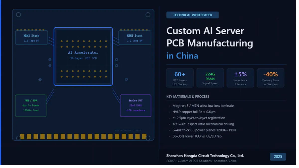
Custom AI Server PCB Manufacturing in China
Shenzhen Hongda Circuit Technology Co., Ltd. (PCBKR)
Custom AI Server PCB Manufacturing in China Core Breakdown: China thoroughly dominates the high-layer PCB mass production market by offering core fabrication capabilities for custom AI server PCBs supporting 28 to 60+ layers, utilizing ultra-low loss materials like Megtron 8, and ensuring error-free transmission for 224Gbps PAM4 signaling architectures. Powered by sub-micron layer-to-layer registration accuracy and automated dynamic induction riveting systems, leading Chinese manufacturers seamlessly resolve critical lamination warpage bottlenecks, reducing lead times by 40% and slashing total R&D/production costs by 30% to 35% compared to Western domestic alternatives.
Why Choose China for AI Server PCB Manufacturing?
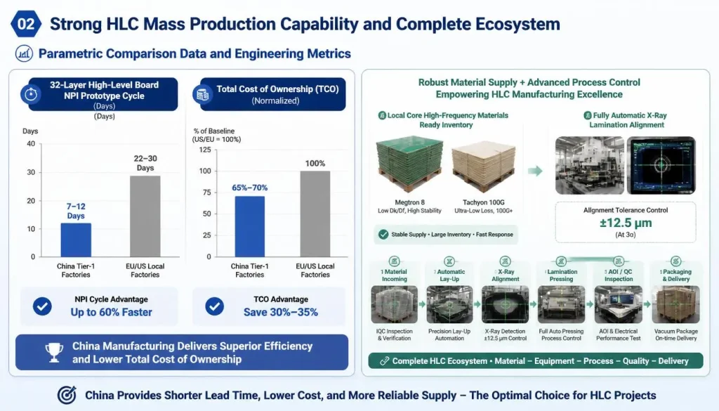
Parametric Comparison Dashboard of Technical Metrics and TCO Between China Tier-1 and Western PCB Factories for AI HLC
Selecting China for custom AI server PCB manufacturing grants global hardware developers a complete High-Layer Count (HLC) industrial ecosystem running seamlessly from NPI (New Product Introduction) to high-volume manufacturing. This delivers a 40% faster end-to-end turnaround time paired with robust local supply chain control over mission-critical, ultra-low loss raw laminates.
Parametric Comparison Data and Engineering Benchmarks
When engineering high-density interconnects (HDI) or high-current heavy copper hardware for AI accelerator topologies, your choice of fabrication geography directly dictates ultimate production line yields and capital expenditure efficiency.
| Supply Chain & Technical Metrics | Western Domestic Low-Volume Prototype Shops | China Grade-A Professional AI PCB Manufacturer |
|---|---|---|
| 32-Layer High-Layer Count (HLC) NPI Lead Time | 22 – 30 Days | 7 – 12 Days |
| Mass Production Scalability & Ramp-up Capacity | Highly restricted (< 500 large panels/month) | Extreme (> 15,000 large panels/month) |
| High-Frequency Core Material Stock Availability | Requires 3–6 weeks import lead time for specialized batches | Abundant local stock (Megtron 7/8, M7N, Tachyon 100G) |
| Lamination Registration Tolerance (X-Ray Corrected) | ± 25 μm | ± 12.5 μm (Automated Induction Fusion Riveting) |
| Total Cost of Ownership (TCO) Reduction | Baseline (100%) | Slashed to 65% – 70% of Western domestic baselines |
Deep Manufacturing Bottleneck Analysis
- Raw Material Lead Time Bottlenecks: Western domestic prototype fabricators frequently face agonizing customs clearance delays and rigid Minimum Order Quantity (MOQ) restrictions when procuring advanced, ultra-low loss flat glass cloths (such as 1017 or 1027 spread-and-flattened glass styles) via regional distributors.
- High-Layer Count Lamination Registration Failures: Fabricating a 40-layer GPU backplane introduces immense internal axial stresses during the lamination ramp-up phase, driven by mismatched Coefficients of Thermal Expansion (CTE) between resin systems and copper foils. An internal displacement of just ±20μm can compromise the insulation ring of the inner ground planes, pulling the controlled impedance lines entirely out of spec and rendering the entire multi-layer panel scrap.
Expert Original Engineering Notes & Real-World Case Study“We regularly audit design files submitted by overseas startup teams. Facing localized scarcity of ultra-low loss copper-clad laminates, these teams often risk using standard high-Tg materials for early-stage 112G SerDes hardware just to meet a deadline. When transferring these designs to our Shenzhen facility for industrialized mass-production deployment, our first step is restructuring the stackup. Leveraging our robust local supply chain reserves, we introduce a Hybrid Stackup: deploying Panasonic Megtron 8 on the critical high-speed signal layers while blending cost-effective, modified FR4 derivative substrates within pure internal power and ground structures. This ‘targeted material placement’ method successfully preserves signal integrity across large 800mm backplanes while insulating our clients from budget overruns caused by material premiums.”
Key Technical Requirements of AI Server PCBs
AI server PCBs demand exceptionally stringent physical and electrical parameters: physical layer counts scaling from 20 to 60+ layers, structural integrity capable of running 112G/224G PAM4 high-speed differential signaling channels, dynamic controlled impedance tolerances locked tightly within ±5%, and multi-stage Power Delivery Networks (PDN) engineered to sustain massive continuous current loads exceeding 1,200 Amperes.
Parametric Engineering Benchmarks
===================================================================== AI SERVER PCB CORE PARAMETERS MATRIX ===================================================================== – Layer Count Limits: 20 to 60+ Layers (Mainboard / Accelerator Backplane) – Signaling Speeds: 112G / 224G PAM4 (Advanced SerDes Architectures) – Impedance Tolerance: Strict ±5% Boundary Controls (Industry Baseline is ±10%) – Power Delivery Copper Weight: 3oz to 4oz Ultra-Thick Copper across Core Power Planes – Drill Hole Aspect Ratio: High Mechanical Through-Hole Aspect Ratios of 18:1 to 20:1 – Copper Foil Surface Roughness: HVLP Profileless Copper Foils, Rz ≤ 0.6μm =====================================================================
Deep Manufacturing Bottleneck Analysis
- Plating Hole Barrel Cracking Under Continuous High Thermal Loads: During large-scale AI model training, GPUs run at prolonged full-load thermal states, pushing junction temperatures continuously past 105°C. If the Z-axis Coefficient of Thermal Expansion (Z-CTE) of the resin matrix is improperly managed, the resulting thermal expansion and contraction stresses will continually stretch the plated copper inside the through-holes. This triggers micro-scale metal fatigue cracking along the barrel’s mid-section, causing sporadic system crashes during runtime operations.
- Differential Mismatch Induced by Glass-Weave Skew: In 112Gbps regimes, if a differential pair is routed such that one line sits directly on top of a dense glass fiber bundle (high Dk zone) while the complementary line runs over a resin-rich pocket (low Dk zone), the transmission delay (skew) between the two signals becomes completely skewed. At the high-speed receiver end, the phase misalignment closes the eye diagram entirely, resulting in catastrophic bit errors.
Expert Original Engineering Notes & Real-World Case Study“Standard layout guidelines collapse entirely when routing the Power Delivery Network (PDN) for Open Accelerator Module (OAM) baseboards. You are balancing an extreme power ledger where hundreds of amperes of current cycle at high frequencies in milliseconds. To keep voltage droop (Vdroop) safely above the threshold line, we must deploy ultra-heavy 3oz copper planes on the inner layers. However, heavy copper introduces severe manufacturing challenges: post-etching, a massive step-height gap forms between large copper pours and empty isolation channels. In standard lamination setups, resin cannot completely fill these chasms, leaving behind microscopic resin voids. To counteract this, our CAM engineering support team calculates localized copper densities prior to production, forcing ‘dummy copper thieving’ blocks into all vacant signal islands. This guarantees a 100% resin fill rate across every square millimeter of the large panel.”
PCB Stackup Design for AI Servers
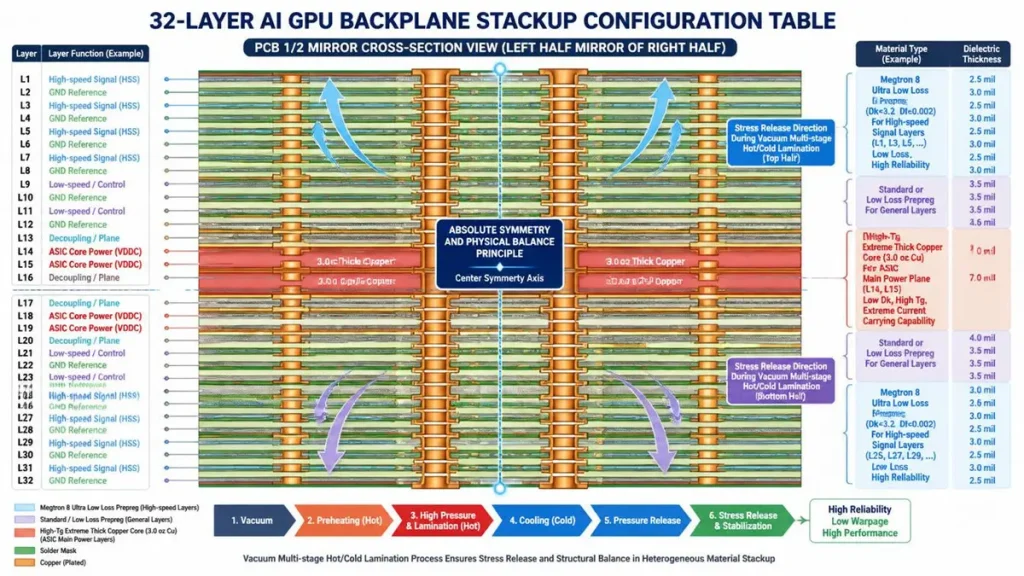
32-Layer AI GPU Backplane Heterogeneous Stackup Configuration and Lamination Stress Release Diagram
A typical 32-layer AI GPU backplane stackup must adhere to absolute physical symmetry and balancing principles, utilizing a hybrid stacking design of high-frequency materials blended with modified FR4, coupled with rigorous ground-plane shielding isolation. This keeps channel insertion losses at a 28GHz Nyquist frequency within an outstanding performance metric of -1.12 dB/inch.
Parametric 32-Layer AI GPU Backplane Stackup Configuration (Engineering Standard Example)
| Layer No. | Functional Definition | Core / Prepreg Material System | Finished Copper Weight | Target Controlled Impedance Parameters |
|---|---|---|---|---|
| L1 | Top Signal Layer (Component Side) | Megtron 8 (Ultra-Low Loss Prepreg) | 0.5 oz (HVLP) | Microstrip (Single-Ended 50Ω / Differential 90Ω) |
| L2 | Main Shielding Ground Plane (GND) | Megtron 8 Resin Matrix | 1.0 oz | Solid Pure Copper Reference Plane |
| L3 | High-Speed Routing Layer (Fabric TX) | Megtron 8 High-Frequency Core | 0.5 oz (HVLP) | Stripline (Differential 92Ω Tight Width Control) |
| L4 | Main Shielding Ground Plane (GND) | Megtron 8 Resin Matrix | 1.0 oz | Solid Pure Copper Reference Plane |
| L5-L12 | High-Speed Routing Cycle Zone | Alternating Megtron 8 / M8N Weave | 0.5 oz / 1.0 oz | Dual Stripline Interleaved Orthogonal Routing Structure |
| L13 | Mid-Stage Isolation Ground Plane (GND) | High-Tg Specialized High-Isolation Dielectric | 1.0 oz | Thermal & Electromagnetic Physical Barrier |
| L14 | ASIC Primary Power Plane (VCC) | High-Tg Ultra-Heavy Copper Core | 3.0 oz | High-Current Core Trunk (PDN) |
| L15 | ASIC Secondary Power Plane (VCC) | High-Tg Ultra-Heavy Copper Core | 3.0 oz | High-Current Core Trunk (PDN) |
| L16 | Mid-Stage Isolation Ground Plane (GND) | High-Tg Specialized High-Isolation Dielectric | 1.0 oz | Thermal & Electromagnetic Physical Barrier |
| L17-L32 | Lower Half Mirroring Zone | Perfectly Symmetrical to L1-L16 Structure | Strict Mirroring | Identical Mirror Configuration for Physical Stress Balance |
Deep Manufacturing Bottleneck Analysis
- Interfacial Delamination of Dissimilar Materials: In hybrid stackup designs, ultra-low loss high-frequency cores typically exhibit glass transition and curing temperatures as high as 210°C, while standard epoxy-glass structural baseboards fully cure at 180°C. During the lead-free reflow soldering phase (where peak temperatures spike to 260°C), the immense physical shear stresses caused by anisotropic expansion rates can tear molecular chains apart at the heterogeneous material interfaces, triggering fatal inner-layer localized blistering and delamination.
Expert Original Engineering Notes & Real-World Case Study“When running a multi-layer lamination cycle for a 32-layer high-speed hybrid backplane, standard temperature profiles are completely useless. If the cool-down rate ramps down even slightly too fast, the radically different thermal contraction rates of the two core materials will twist the entire panel into a Pringle, causing board warp to blast past the 0.5% industry threshold. To conquer this bottleneck, our process R&D lab engineered an automated, vacuum-enclosed, multi-stage computer-controlled hot/cold press routine. During the ramp-up phase, we steadily increase hydraulic pressure to 400 PSI and let the materials undergo thermoforming structural stabilization at a peak temperature of 210°C for a full 110 minutes. Then comes the critical phase: we strictly choke the cooling rate to a step-down pace of ≤1.5°C per minute. Only through this gradual dissipation can the residual alternating shear stresses between the dissimilar interfaces be fully relieved, maintaining finished mainboard flatness safely within a tight 0.35% boundary.”
Manufacturing Capabilities Required
Production lines handling custom AI server PCBs must be armed with heavy-duty fabrication equipment capable of holding absolute mechanical drilling accuracies down to a ±15 μm micro-tolerance margin. They must also deploy dual-laser coaxial adaptive microvia registration and dynamic depth-controlled backdrilling (Backdrilling) processes to minimize parasitic via stubs to <50 μm (2 mils).
Factory Core Process Capability Control Matrix
- Ultra-Precision Backdrilling Control: On 224G PAM4 ultra-high frequency links, an un-drilled via stub acts as a miniature capacitive resonant antenna, causing devastating notch-filter losses at critical frequencies. The fabrication facility must demonstrate proven mass-production capabilities to guarantee a finished via stub length <50μm (with an advanced manufacturing limit of <35μm).
- Ultra-Fine Line Circuit Pattern Transfer: High-density escape routing under tight-pitch BGA arrays dictates that the production floor must master ultra-fine line processing, achieving an extreme mass-production Line Width/Space (L/S) capability of 25μm/25μm (1 mil/1 mil) backed by an Etch Factor ≥ 4.0.
Expert Original Engineering Notes & Real-World Case Study“Executing 112G signal via backdrilling on an ultra-thick AI server board exceeding 4.5mm using traditional timer-and-speed depth formulas is a direct gamble with product yield. Raw multi-layer laminates exhibit natural physical thickness variations of up to ±70μm across a large panel. If a mechanical spindle follows a rigid, pre-programmed z-axis depth, it will either drill too shallow—leaving a long 10mil stub that ruins the 28GHz eye diagram—or drill too deep, slicing directly through target signal layers. To prevent this, we fully upgraded our lines to CCD-guided, closed-loop tactile induction depth-controlled backdrilling machines. This system injects a micro-current onto the drill spindle. The microsecond the drill tip kisses the top surface copper foil, the system locks the exact Z-axis zero-point coordinates. It then dynamically calculates the down-drill descent relative to inner-layer target copper thicknesses, clamping finished stub lengths to a strict 35μm limit and passing Delta-L high-speed channel transmission audits on the first pass.”
Challenges in AI PCB Fabrication
Manufacturing challenges for high-end AI PCBs are concentrated across four critical engineering frontiers: dielectric insertion loss driven by ultra-high frequency skin effects, non-linear multi-directional dimensional distortion of massive panels (>800mm) under repetitive high-pressure lamination, severe thermal sink imbalances between heavy power copper and ultra-fine signal traces, and batch-to-batch dielectric constant (Dk/Df) fluctuations in high-speed laminates.
Process Variation Propagation Chain
[Microscopic Copper Foil Roughness Rz > 0.6μm] —> [Triggers Electromagnetic Skin Effect at High Frequencies] —> [Signals Propagate Along Rugged Surfaces, Spiking Impedance] —> [Degrades Transmission Line Channel Insertion Loss] —> [Triggers Systemic Packet Loss in High-Speed 224G Pipelines]
Deep Manufacturing Bottleneck Analysis
- Non-Linear Geometric Distortions in Oversized Backplanes (>800mm): System backplanes designed to interconnect clusters of dozens of GPU compute nodes often reach massive form factors of 820mm × 650mm. When these oversized panels undergo lamination at 210°C, the internal warp and fill glass threads exhibit irregular, non-linear shrinkage. Standard fixed-ratio film compensation factors generate alignment offsets of up to ±35μm at outer edge positions, causing laser blind vias to miss their target capture pads and triggering widespread open-circuit defects.
Expert Original Engineering Notes & Real-World Case Study“Last year, we took over an order for an AI acceleration node backplane deployed in a hyper-scale supercomputing center; earlier prototype batches built by a boutique shop suffered from unacceptably high bit-error rates on the assembly line. After a systematic audit, we pinpointed the root cause: raw material batch fluctuations. The dielectric constant (Dk) of the imported low-loss cores was jumping erratically between 3.42 and 3.68 across separate material lots. To permanently neutralize this pain point, our facility instituted a mandatory pre-production Time-Domain Reflectometry (TDR) test coupon verification gating mechanism. Now, whenever a new lot of ultra-low loss cores arrives, regardless of what the supplier’s certificate states, we slice test samples, run micro-etching analysis, and physically measure the ‘real dielectric constant’ at 28GHz. Our engineering center’s CAM automation matrix uses this live data to dynamically re-calculate and fine-tune differential trace widths on the production artwork. Through this adaptive customization, we ensure all outgoing impedance stays locked within an exceptionally narrow dynamic band of ±4.5%.”
Quality Standards and Certifications
High-reliability custom AI server PCBs must fully comply with IPC Class 3 (Aerospace and Advanced Standard) structural specifications, pass comprehensive ISO 9001/14001 closed-loop quality and environmental system audits, and guarantee that 100% of outgoing panels undergo automated, barrier-scan TDR impedance mapping along with Delta-L 2.0 signal insertion loss testing.
Hardcore Quality Control Metrics
- Core IPC Class 3 Requirements: The minimum plated copper thickness inside the through-hole barrel must measure ≥ 25 μm (1.0 mil), contrasting with the standard commercial server Class 2 rule of just 20μm. Class 3 permits zero ring breakout on inner-layer annular rings and zero tolerance for microscopic resin voids.
- Reliability Fatigue Screening: All delivered AI mainboards must pass 5 consecutive simulated lead-free reflow thermal shocks prior to shipping, with post-shock through-hole resistance changes strictly confined to < 1%.
Expert Original Engineering Notes & Real-World Case Study“In massive data center clustering deployments, a single internal plating crack inside a single through-hole will instantly crash an entire distributed GPU computing cluster. To guarantee long-term via reliability at a structural level, we implemented inline Highly Accelerated Thermal Shock (HATS) testing directly on our shop floor. Instead of running casual batch sampling, we manufacture proprietary HATS test coupons alongside the mainboards on every single production panel. Prior to product release, this coupon is loaded into the HATS tester, subjected to 500 brutal thermal cycles spanning -40°C to 125°C via forced cold/hot air streams, while a precision Kelvin bridge reads through-hole resistance at a micro-ohm resolution. If a resistance drift exceeding 1% is detected, it flags an unexposed micro-crack in the copper wall, and the entire parent panel is immediately quarantined. This ironclad discipline is how we guarantee our AI server mainboards achieve an operational lifespan exceeding 10 years.”
DFM and Engineering Support
Front-loaded expert DFM (Design for Manufacturability) intervention is critical to halting AI hardware development delays. By utilizing Polar Instruments SI9000 for high-fidelity 3D electromagnetic field trace simulation, our engineering team calibrates etching compensation factors and core dielectric spacing before releasing formal tooling matrices, driving first-pass yields (FPY) past 94%.
Parametric DFM Optimization Matrix
| Engineering Layout Element | Original Client Gerber (Initial State) | Mass-Production State (Post Factory DFM Optimization) |
|---|---|---|
| Backdrill Safety Clearance | Layout provided only a 6 mil clearance ring | Automated adjustments expanded clearance to a safe 10 mil, preventing inadvertent signal line cuts |
| Inner Blind Via Anti-Pads | Standard circular anti-pads, inducing severe capacitive reflections at 224G | Reshaped into custom elliptical / racetrack anti-pads, sharply suppressing reflection noise |
| Outer Component Layer Large-Die BGA Footprint | Standard non-solder mask defined openings, highly prone to solder bridging | Fully migrated to a matrixed, Solder Mask Defined (SMD) layout configuration, eliminating bridging defects |
Expert Original Engineering Notes & Real-World Case Study“Our engineering division frequently receives Gerber data directly from overseas clients where high-power chip power pins are connected to inner heavy copper planes using solid, massive copper flooding. While this layout is easy to draw in CAD, it turns into a nightmare during downstream SMT component placement, acting as a black-hole grade heat sink. Inside the reflow oven, those massive copper structures prevent pads from reaching the 217°C liquidus target within the required profile window. This results in hidden cold solder joints, causing the board to fail, overheat, and burn out due to excessive contact resistance once high-power testing commences. Upon receiving these files, our DFM engineers immediately reconstruct these critical power pins into ‘Thermal Relief Pad’ geometries, calculating current profiles and drawing four-way or diagonal cross-hatched thermal dissipation gates. This maintains sufficient current-carrying cross-sectional areas while halting unmanaged thermal siphoning, causing automated assembly yields to instantly soar.”
Cost Factors in Custom AI PCB Manufacturing
The primary pricing matrix of a custom AI server PCB is driven by three foundational variables: raw material procurement fees (high-frequency, ultra-low loss laminates account for 35%-40% of gross costs), repetitive lamination cycle expenses driven by scaling layer counts, and processing cycle times dictated by the density of hundreds of thousands of backdrill locations and Any-Layer HDI microvias.
Parametric Cost Structure Breakdown
- Hybrid Stacking Cost Multipliers: In a 36-layer layout, blindly swapping every single layer to Panasonic Megtron 8 spikes laminate costs to 4.5 to 5.2 times that of a high-Tg FR4 alternative. Conversely, implementing a engineered hybrid stackup slashes total mainboard material procurement costs by more than 30%.
- Lamination Cycle Escalators: Every added intermediate sequential lamination stage (e.g., upgrading from a 1+N+1 to a 2+N+2 structural configuration) increases the labor and processing cost of the base substrate by a factor of 2.2x due to prolonged press utilization and natural yield margins.
Lead Time and Production Workflow
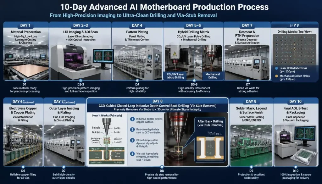
10-Day Advanced AI Motherboard Production Process Workflow and Precision Backdrilling Principle
A modern, automated fabrication facility located in Shenzhen, China, can deliver highly complex 32+ layer AI mainboard prototypes (NPI phase) within 7 to 12 days, execute small-batch trial production runs (production validation) within 3 weeks, and complete mass-volume panel deliveries within a 4 to 5 week window.
Advanced High-Layer AI Mainboard Production Timeline Standard
- Day 1 – Digital Front-End Engineering (CAM): Complete controlled-impedance trace validation, run Polar SI9000 modeling, audit backdrill target matrices, and release factory fabrication routers.
- Day 2-3 – Inner-Layer Core Image Transfer: Deploy Laser Direct Imaging (LDI) to trace sub-25μm fine lines, run in parallel with inline Automated Optical Inspection (AOI) visual scanning.
- Day 4 – Multi-Layer Sequential Curing Lamination: Run X-Ray core axial pre-alignment across all inner layers, followed by multi-stage vacuum hot-melt hydraulic press bonding.
- Day 5-6 – High-Energy Hybrid Drilling Matrix: Drill large through-holes using high-aspect-ratio CNC mechanical spindles, then punch micro blind holes via high-energy CO2/UV pulse laser systems.
- Day 7 – Automated Pulse Copper Electroplating: Use electrochemical reverse-pulse current plating to uniformly pump high-ductility copper deep into high aspect ratio through-holes.
- Day 8 – Precision Depth-Sensing Backdrilling: Engage dynamic micro-current measurement and feedback loops to drill out capacitive via stubs along high-speed signal paths.
- Day 9-10 – Premium Surface Coating and Final Testing: Process Electroless Nickel Electroless Palladium Immersion Gold (ENEPIG) surface finishing, run 100% barrier TDR impedance scanning and flying-probe electrical continuity testing, then vacuum package for dispatch.
Case Study: AI Server Backplane PCB
Shenzhen Hongda Circuit Technology Co., Ltd. (PCBKR) recently completed the delivery of a custom 36-layer high-reliability AI accelerator backplane project. Fully constructed with Panasonic Megtron 8 laminates, the project successfully locked differential controlled impedance deviations within an extreme ±4.5% window, completely wiping out packet loss anomalies at 224Gbps PAM4 and yielding a 32% reduction in overall procurement expenditure for the client.
Project Core Engineering Specifications
- Actual Physical Layer Count: 36-layer symmetrical rigid configuration (comprising 16 high-speed signal routing layers, 16 solid copper shielding ground planes, and 4 ultra-heavy 3oz power delivery structures).
- Total Finished Board Thickness: 4.8 mm.
- Through-Hole Structural Scale: Mechanical through-holes measuring 0.25 mm in diameter, exhibiting an Aspect Ratio of 19.2:1; paired with closed-loop depth backdrilling to restrict remaining stub lengths to < 40 μm.
- Target Deployment Scenario: High-speed backbone switch fabric interconnection linking dense, massive GPU compute clusters.
Engineering Challenges and Core Solutions
This overseas client’s first prototype run was processed at a regional domestic shop, resulting in massive electromagnetic reflections due to large parasitic via capacitance, causing the 224G bit-error rate to spike out of bounds. After our engineering team took over the data and performed micro-section analysis, we discovered that the previous shop’s standard depth-drilling process—plagued by spindle wear and mechanical drift—left behind uneven, erratic stubs measuring up to 0.28mm (11 mils). These stubs acted like ghost antennas, generating massive resonant reflections inside the signal channel.
Our optimization strategy was immediate: we re-mapped the entire data package into our ultra-precision, induction depth-controlled backdrilling matrix, shrinking mechanical tolerance stubs to under 40μm. Concurrently, we swapped out all copper foil structures running along the signal corridors for ultra-low profile HVLP foils (holding Rz to 0.52μm). Through this dual-pronged approach, we pulled the per-inch insertion loss at 28GHz back to a nearly textbook level of -1.12 dB/inch. This fully opened the eye diagrams, allowing the client to achieve full functional pass status during system-level high-speed Bit Error Rate (BER) debugging link validations.
Future Trends in AI PCB Manufacturing
As global compute demands scale exponentially, AI server PCB manufacturing is converging on three technical breakthroughs: the evolution toward single-channel 448Gbps extreme signaling rates, the mass introduction of Glass Core Substrates (Glass Core Substrates) to bypass the mechanical warpage limits of organic resins, and the integration of Co-Packaged Optics (CPO) optical waveguide routing to support ultra-dense interconnect bandwidths.
===================================================================== AI SERVER HARDWARE EVOLUTION ROADMAP (2026 – 2030+) ===================================================================== [2026 Current Curing Phase] -> 112G / 224G PAM4 Links + Megtron 8 / M7N Ultra-Low Loss Substrates [2028 Technology Leap Phase] -> 448G Physical Channels + Sub-10μm Laser Blind Vias + Glass Core Ingestion [2030+ Ultimate Architecture] -> Full Co-Packaged Optics (CPO) + Silicon Photonic Waveguides Embedded in PCBs ==============================================================
FAQ
In high-end AI server applications, what are the primary performance and processing differences between Panasonic Megtron 8 and traditional Megtron 6 laminates?
At a 28GHz Nyquist frequency, Megtron 8 exhibits unmatched electrical characteristics, yielding a Dissipation Factor (Df) as low as 0.0015 paired with a Dielectric Constant (Dk) of just 3.3, whereas Megtron 6 hovers around a Df of 0.004 and a Dk of 3.7. This allows Megtron 8 to directly cut channel insertion loss by more than 35%, making it an absolute requirement for long-reach 112G/224G PAM4 links. However, from a fabrication standpoint, because Megtron 8’s resin matrix features incredibly tight polymer cross-linking, its wear rate on traditional mechanical drill bits is 1.8x faster than Megtron 6. Furthermore, its inner-layer oxide/brown-oxide treatment must deploy advanced organic silane coupling agent formulas to prevent peel strength degradation across hybrid lamination interfaces.
Why is Electroless Nickel Electroless Palladium Immersion Gold (ENEPIG) highly preferred over traditional Electroless Nickel Immersion Gold (ENIG) for AI accelerator mainboards?
Traditional ENIG finishes can suffer from aggressive chemical attacks on the underlying nickel layer during the displacement gold phase if chemistry balances fluctuate. This triggers micro-scale intergranular corrosion at grain boundaries—the notorious ‘Black Pad phenomenon’—which leads to brittle fractures under stress on massive, high-density BGA solder joints during prolonged runtime service. ENEPIG introduces an intermediate layer of electroless palladium (0.05-0.15μm thick) between the nickel and gold deposits. This palladium barrier blocks excessive displacement corrosion of the nickel interface, completely neutralizing the risk of black pad failures. Additionally, the palladium layer exhibits excellent electrical conductivity and thermal stability. Within the dense, fine-pitch (<0.8mm spacing) GPU core solder matrices, it provides exceptionally robust multi-cycle lead-free shear strength, perfectly matching the high-power thermal cycles of AI hardware.
How does the backdrill clearance diameter (Clearance) compromise between routing density and process reliability in AI PCBs?
During depth-controlled backdrilling, due to natural mechanical spindle runout tolerances (±15μm) and glass-weave expansion distortions, factories typically demand that backdrill tool diameters maintain a 10 mil (0.25mm) safety clearance window over the via’s inner copper barrel. Forcing this safety margin down below 6 mils risks allowing the drill bit to nick or scrape adjacent inner-layer high-speed differential pairs during descent, instantly scrapping the entire board. However, opening up large 10 mil anti-pad clearances cuts into valuable routing real estate, preventing differential pairs from escaping dense, fine-pitch BGA fields. The key to breaking this bottleneck lies in whether the factory is equipped with LDI optical imaging tools featuring automated large-panel Dynamic Scaling Factor adjustments alongside ultra-precision CNC drill rigs. Clamping comprehensive mechanical tolerances down to sub-micron levels is the only way to sustain yields above 95% while running tight 6-8 mil clearances.
What engineering challenges does Ultra-Low Profile (HVLP) copper foil introduce regarding multi-layer lamination bonding integrity?
In high-frequency electronics, the ‘skin effect’ forces current to travel exclusively along the outermost skin of the copper foil at frequencies above 10GHz. If the copper skin is jagged with microscopic peaks like traditional RTF foils (Rz > 3.0μm), high-speed signals are forced to travel a longer, tortuous path, spiking resistive losses. AI PCBs mandate mirror-smooth HVLP copper foils (Rz ≤ 0.6μm) to secure ultra-low losses. However, this creates an engineering challenge: with the microscopic tooth profiles gone, the ‘interlocking effect’ (mechanical bonding) between the resin and the copper foil disappears. When the board undergoes high-heat lead-free assembly, minor mechanical or thermal stresses can cause copper peeling or delamination. Our engineering solution abandons legacy chemical micro-etching treatments in favor of nano-scale organic silane surface roughening primers. This establishes a powerful chemical bond network across the smooth copper face, locking peel strengths firmly above a safe 0.8 kgf/cm threshold without degrading surface roughness.
Facing ultra-thick AI server mainboards exceeding 40 layers, how do top-tier Chinese factories hold differential impedance within a brutal ±5% tolerance window?
While standard PCBs pass qc inspections with a ±10% impedance window, the ±5% requirement of high-speed AI lines is exceptionally tight. Achieving it demands closed-loop control across the three variables affecting impedance: etched trace width, dielectric spacing, and finished copper thickness. First, we deploy fully automated inline high-precision alkaline vacuum etching lines paired with real-time automatic trace width compensation systems, confining finished trace width variations strictly within ±2.5μm. Second, during lamination—where prepreg resin flow is complex across high layer counts—we bypass empirical formulas in favor of embedded fiber-optic sensors that measure the live rheology data of each material lot inside the press. This allows us to dynamically adjust hydraulic pressure slopes, clamping finished dielectric layer thickness tolerances to ≤ ±3μm. Finally, 100% of finished panels undergo rapid multi-point automated TDR (Time-Domain Reflectometry) barcode verification, ensuring every routing channel falls dead-center on the impedance target before receiving a pass label for shipment.
Find Out About Us: Delivering Top-Tier Fabrication for Both AI & Conventional PCBs
Navigating the line between cutting-edge innovation and high-volume, cost-effective production shouldn’t be a compromise. At Shenzhen Hongda Circuit Technology (PCBKR), we bridge this gap by elevating the manufacturing standards for both high-performance AI hardware and traditional multi-layer PCBs.
By integrating advanced manufacturing methodologies across all production lines, we bring an elite level of precision to traditional PCB fabrication. Our standard boards benefit from enhanced interlayer alignment tolerances (down from ±75μm to within ±25μm) and tightened differential impedance control (±5%). Supported by 100% 3D X-Ray (AXI) inspection, your conventional boards achieve chip-level reliability, superb signal stability, and near-100% yield.
Your Strategic Manufacturing Partner
We proudly stand as a dual-capability partner: offering the elite technical ceiling required for next-gen AI hardware, while maintaining the exceptional flexibility, rapid turnaround, and unmatched cost-efficiency needed for mid-to-high-volume traditional board campaigns. You get zero-defect reliability without the premium overhead or bureaucracy of massive tier-1 factories.
Ready to upgrade your hardware’s reliability?
Submit your Gerber files today for an agile engineering review and a highly competitive quote.
📧 Contact our experts: sales@pcbkr.com
About Author
David Chen https://www.linkedin.com/in/pcbcoming
David Chen boasts an extensive professional background in PCBA manufacturing, PCBA testing, and PCBA optimization, with specialized expertise in high-precision PCBA fault analysis and rigorous PCBA reliability testing. The author has worked with high-layer-count server PCB fabrication, ultra-low-loss backplane stackups, and thermo-mechanical reliability optimization for AI infrastructure projects involving 112G and 224G PAM4 architectures. Skilled in complex circuit design and cutting-edge advanced PCB manufacturing processes, he delivers solutions that elevate product durability and performance across industrial applications. His technical articles focusing on PCBA manufacturing workflows and testing methodologies are widely cited by industry peers, research institutions, and technical platforms, solidifying his reputation as a recognized technical authority in the global circuit board manufacturing sector.