Aerospace & Defense PCB Manufacturing & Assembly Technical Guide
Advanced Substrate Engineering, High-Reliability Fabrication, and Class 3/3A Assembly Standards
1.Aerospace PCB Manufacturing Executive Summary & Industry Context
Printed circuit boards (PCBs) and printed circuit board assemblies (PCBAs) used in aerospace, defense, and space-flight applications demand the highest levels of reliability, operating in environments defined by extreme thermal cycling, mechanical shock, vibration, and high vacuum.
Unlike commercial or consumer electronics where cost and miniaturization are key drivers, Aerospace & Defense (A&D) hardware focuses on long-term operational integrity and zero-defect performance under extreme operating conditions.
Aerospace & Defense Hardware Mandates
- Zero-Defect Manufacturing: Mandatory compliance with IPC Class 3 or Class 3A standards.
- Extended Thermal & Mechanical Reliability: Continuous operation across extended temperatures (-55°C to +125°C+).
- Vacuum Outgassing Compliance: Strict material limits in space environments (TML < 1.0%, CVCM < 0.1%).
- Severe Environmental Resistance: Built to withstand extreme vibration and structural loads.
- Strict Traceability & Quality Systems: Full lifecycle control certified to AS9100D.
2. Market Dynamics & Core Design Requirements
2.1 Market Growth Drivers
The global Aerospace & Defense PCB/PCBA market is driven by several key factors:
- Satellite Constellation Expansion: Growing demand for Low Earth Orbit (LEO) satellite constellations requires high-density, low-outgassing high-frequency substrates.
- Defense Electronics Modernization: Radar systems, electronic warfare (EW), guided munitions, and avionics require advanced RF and high-speed digital designs.
- Commercial Aviation Upgrade: Modern aircraft avionics demand higher processing power and lighter weight, driving adoption of High-Density Interconnect (HDI) and Rigid-Flex architectures.
2.2 Core Technical Specifications Comparison
| Parameter | Aviation & Commercial Avionics | Defense & Missile Electronics | Deep Space / Orbital Satellite |
| Industry Baseline Class | IPC-6012 Class 3 | IPC-6012 Class 3 / MIL-PRF-31032 | IPC-6012 Class 3A / Space Addendum |
| Operating Temp Range | -55°C to +125°C | -55°C to +150°C | -65°C to +150°C (Thermal Cycling) |
| Outgassing Requirement | Standard | Standard | Mandatory: TML < 1.0%, CVCM < 0.1% |
| Impedance Tolerance | ±10% (Standard) / ±5% (Precision) | ±5% (Precision Controlled) | ±5% (Precision Controlled) |
| Min Trace / Space (PCB) | 75 μm / 75 μm (3 mil / 3 mil) | 50–75 μm (2–3 mil) | 50–75 μm (2–3 mil) |
| Plating Copper Thickness | Minimum 25 μm (1.0 mil) average | Minimum 25–30 μm | Minimum 25 μm (In-hole copper) |
3. Applicable Standards & Qualification Framework
To ensure mission success, aerospace PCB manufacturing and assembly strictly adhere to specialized qualification frameworks:
3.1 Quality Management Systems
- AS9100D: Quality Management Systems – Requirements for Aviation, Space, and Defense Organizations.
- NADCAP: National Aerospace and Defense Contractors Accreditation Program for special processes (chemical processing, electronics, heat treating).
3.2 Bare PCB Manufacturing Standards
- IPC-6012 Class 3 / Class 3A: Qualification and Performance Specification for Rigid Printed Boards (Class 3A includes IPC-6012DS/ES Space and Military Avionics Applications Addendum).
- IPC-6013 Class 3: Qualification and Performance Specification for Flexible/Rigid-Flex Printed Boards.
- MIL-PRF-31032: Performance Specification for Printed Wiring Boards (US Military).
- ECSS-Q-ST-70-60C: European Cooperation for Space Standardization – Materials and processes for space PCB manufacturing.
3.3 PCBA Assembly Standards
- IPC-A-610 Class 3: Acceptability of Electronic Assemblies (High Performance/Harsh Environment Electronics).
- IPC-J-STD-001 Class 3 / Space Addendum: Requirements for Soldered Electrical and Electronic Assemblies.
- NASA-STD-8739: NASA Workmanship Standards for Soldering, Cable/Harness, and Conformal Coating Assembly (PCBA level).
4. Substrate & Material Selection
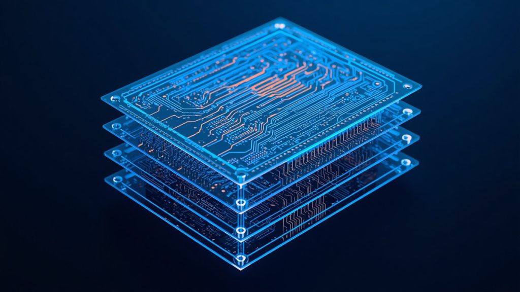
Unveiling the Core: Inside the Multilayer HDI PCB Stackup Design for High-Reliability Avionics
The choice of dielectric material is critical to withstand high thermal stress and prevent delamination or signal degradation.
A&D Substrate Selection Matrix
- High-Tg FR-4: Delivers extended thermal stability with Tg ≥ 170°C.
- Polyimide: Offers extreme thermal resistance with Tg ≥ 250°C for high-heat environments.
- PTFE / Ceramic Hydrocarbon: Used for RF and microwave high-frequency designs requiring exceptionally low Dk and Df.
- Low-Outgassing Dielectrics: Essential for orbital space and high-vacuum applications.
4.1 Key Dielectric Properties
- High Glass Transition Temperature ($T_g$): Materials must maintain structural stability. High-Tg FR-4 ($T_g \ge 170^\circ\text{C}$) and Polyimide ($T_g \ge 250^\circ\text{C}$) are widely specified.
- Decomposition Temperature ($T_d$): $T_d \ge 340^\circ\text{C}$ is required to withstand multiple thermal excursions during assembly and rework.
- Low Coefficient of Thermal Expansion (CTE): $Z$-axis CTE must be minimized (typically $< 3.5\%$ up to $T_g$) to prevent Plated Through-Hole (PTH) barrel cracking during thermal shocks.
4.2 Material Classifications
| Material Category | Examples | Key Parameters | Typical Applications |
| High-Tg Polyimide | Ventec VT-901, Arlon 85N | Tg ≥ 250°C, High Thermal Stability | Engine Controls, High-Temp Military Avionics |
| High-Tg Advanced FR-4 | Isola 370HR, Shengyi S1000-2M | Tg ≥ 170°C, High Reliability | Defense Avionics, Power Distribution Modules |
| Ultra-Low Loss Substrates | Panasonic Megtron 6 / Megtron 7 | Tg 185°C–200°C, Ultra-low Dk/Df | High-Speed Digital, Radar Signal Processing |
| High-Frequency PTFE/Hydrocarbon | Rogers RO4000 Series, Taconic TLY | Low Dk (2.15–3.50), Low Df (< 0.003) | RF Communication, Phased Array Radar, Satellite Payload |
5. Advanced Fabrication & Mechanical Engineering
5.1 High-Precision Drilling & Microvia Creation

High-Precision Laser Microvia Technology for IPC Class 3 HDI Aerospace PCBs
- Mechanical Micro-Drilling: High-speed CNC drilling machines equipped with air-bearing spindles operating up to 200,000–350,000 RPM are utilized for micro-drill diameters down to 0.10–0.15 mm.
- Laser Microvia Drilling: UV and $\text{CO}_2$ pulsed lasers are used for blind/buried microvias in HDI stackups, operating at high pulse rates (typically 1,000–3,000 holes/sec) to achieve clean dielectric ablation.
5.2 Copper Plating & Hole Integrity
IPC Class 3 and Class 3A require robust plating integrity:
- Minimum Average Copper Thickness: 25 μm (1.0 mil) in PTH walls to resist thermal expansion stresses.
- Zero Wrap Plating Failures: Continuous surface-to-hole copper transitions without voids or thin spots.
- Etch Back / Desmear: Plasma desmear or chemical etch-back is required to ensure clean inner-layer interconnects before plating.
6. Precision Controlled Impedance
For high-frequency RF and high-speed digital signals (e.g., radar, optical links), impedance matching is crucial.
6.1 Process Capabilities
- Standard Control: ±10% tolerance across the manufacturing lot.
- Precision Control: ±5% tolerance achieved through strict dielectric thickness control, automated optical inspection (AOI) of trace geometry, and differential etching process controls.
7. High-Reliability PCBA Assembly & Inspection
7.1 Advanced SMT & Reflow Process
- Vacuum Nitrogen Reflow: Vacuum-assisted reflow soldering is employed for power electronics and high-reliability BGA components to reduce solder voiding.
- Solder Joint Voiding Limits: Aligned with IPC Class 3 standards, overall solder voiding on critical power components and BTCs is controlled to ≤ 15% (with single voids ≤ 9%), ensuring superior thermal dissipation and mechanical strength.
Assembly Quality Note: Switching from standard reflow to vacuum-assisted reflow consistently reduces solder void rates from 15%–25% down to under 10%, drastically improving thermal dissipation and reliability under thermal cycling.
7.2 Conformal Coating & Potting
Ultraviolet (UV) Inspection of Conformal Coating on Aerospace PCBA Assembly
To protect assembled circuit boards against moisture, salt spray, and fungal growth:
- Coating Types: Polyurethane (UR), Acrylic (AR), Epoxy (ER), and Silicone (SR) per IPC-CC-830 or MIL-I-46058C.
- Parylene (XY): Vapor-deposited coating used for space-grade applications requiring ultra-thin, pinhole-free coverage.
8. Environmental Verification & Quality Control
Every aerospace PCB/PCBA batch undergoes rigorous screening before deployment:
| Inspection / Test Item | Purpose & Standard Alignment |
| Microsectioning / Cross-Section Analysis | Evaluates hole wall copper thickness, registration, and internal layer integrity per IPC-6012. |
| Thermal Stress Testing | Solder float testing at 288°C (IPC-TM-650 Method 2.6.8) to verify dielectric delamination resistance. |
| Thermal Cycling & Thermal Shock | Evaluates thermal expansion endurance across extreme gradients (-55°C to +125°C+). |
| Outgassing Screening | Verifies TML < 1.0% and CVCM < 0.1% per ASTM E595 for orbital/space vacuum environments. |
| X-Ray Inspection (AXI) & Testing | Validates solder joint integrity, BGA wetting, and electrical continuity per IPC-A-610 Class 3. |
9. Conclusion
Aerospace and defense electronics require uncompromising engineering discipline from substrate selection to final assembly verification. By strictly following AS9100D, IPC Class 3/3A, and MIL-PRF-31032 standards, manufacturers can deliver ultra-reliable circuit assemblies capable of performing flawlessly in the harshest mission-critical environments.
Frequently Asked Questions (FAQ)
What is the main difference between IPC Class 3 and IPC Class 3A for aerospace PCBs?
IPC Class 3 applies to High-Performance Electronic Products where continued high performance or performance-on-demand is critical, such as military avionics and medical systems.
IPC Class 3A (which includes the IPC-6012DS/ES Space and Military Avionics Applications Addendum) imposes even stricter requirements specifically for spaceflight hardware, including thicker minimum hole-wall copper plating (typically ≥ 25 μm), tighter annular ring tolerances, and mandatory thermal stress microsectioning.
Why is ASTM E595 outgassing compliance mandatory for space-grade PCBs?
In the vacuum of space, volatile organic compounds (VOCs) and moisture trapped in PCB substrates or conformal coatings can evaporate (outgas). These vaporized molecules can condense onto critical optical sensors, solar panels, or high-voltage circuits, causing optical blinding or electrical shorting.
To prevent this, space-grade materials must meet ASTM E595 screening limits:
Total Mass Loss (TML): $< 1.0\%$
Collected Volatile Condensable Material (CVCM): $< 0.1\%$
What impedance tolerance can realistically be achieved in high-reliability aerospace manufacturing?
While standard commercial PCBs typically target a ±10% impedance tolerance, precision aerospace and defense designs (such as high-frequency radar feedlines or high-speed differential pairs) target ±5%.
Achieving ±5% requires precise control over dielectric thickness tolerances, dielectric constant ($D_k$) uniformity, trace etching profile accuracy via automated optical inspection (AOI), and precise copper foil weighing. Achieving tolerances tighter than ±5% across volume production is generally cost-prohibitive and unnecessary for most mission requirements.
Can NASA-STD-8739 be used as an inspection standard for bare PCB fabrication?
No. NASA-STD-8739 series standards (such as 8739.1, 8739.4) govern assembly workmanship—specifically hand soldering, cable/harness assembly, and conformal coating application on populated board assemblies (PCBAs).
Bare PCB manufacturing must be qualified and inspected against bare-board specifications such as IPC-6012 Class 3/3A (IPC-6012ES), MIL-PRF-31032, or ECSS-Q-ST-70-60C.
How does vacuum reflow soldering improve solder joint reliability in aerospace PCBAs?
During standard reflow soldering, trapped flux vapors and air can form voids inside the solder joint, particularly under large thermal pads of power devices or Bottom-Terminated Components (BTCs). High voiding percentages (> 20%) reduce thermal conductivity and create mechanical stress concentration points during thermal cycling.
Vacuum reflow chambers draw a vacuum during the liquidus phase of the solder, pulling out trapped gas bubbles and consistently reducing total void ratios to ≤ 10%, well within the IPC Class 3 requirement of ≤ 15%.
Why is Polyimide preferred over High-Tg FR-4 in engine control unit (ECU) applications?
Although High-Tg FR-4 ($T_g \ge 170^\circ\text{C}$) performs exceptionally well in avionics bays, engine control units and missile thrust vectoring electronics operate in continuous ambient temperatures exceeding 150°C to 200°C.
Polyimide substrates offer an ultra-high Glass Transition Temperature ($T_g \ge 250^\circ\text{C}$) and superior resistance to thermal degradation ($T_d \ge 380^\circ\text{C}$), preventing substrate softening, Z-axis expansion cracking, or delamination under continuous high thermal loads.
About Shenzhen Hongda Circuit Technology Co., Ltd.
Shenzhen Hongda Circuit Technology Co., Ltd. (PCBKR) is a premier global manufacturer specializing in high-reliability PCB fabrication and PCBA assembly for Aerospace, Defense, Telecom, and High-Speed Computing sectors.
Our Core Capabilities:
- Certifications: AS9100D, ISO 9001, ISO 14001, and UL Certified.
- Manufacturing Standards: Full compliance with IPC Class 3 / Class 3A (IPC-6012DS/ES Space Addendum) and MIL-PRF-31032.
- Advanced Substrates: Specializing in High-Tg Polyimide (Ventec VT-901, Arlon 85N), Rogers, Taconic, Megtron 6/7, and Heavy Copper laminates.
- Precision Engineering: ±5% impedance control, laser microvia drilling, plasma desmear, and vacuum nitrogen reflow assembly.
For engineering inquiries, stackup consultation, or RFQ support:
- Email: sales@pcbkr.com
About Author
David Chen https://www.linkedin.com/in/pcbcoming
David Chen boasts an extensive professional background in PCBA manufacturing, PCBA testing, and PCBA optimization, with specialized expertise in high-precision PCBA fault analysis and rigorous PCBA reliability testing. The author has worked with high-layer-count server PCB fabrication, ultra-low-loss backplane stackups, and thermo-mechanical reliability optimization for AI infrastructure projects involving 112G and 224G PAM4 architectures. Skilled in complex circuit design and cutting-edge advanced PCB manufacturing processes, he delivers solutions that elevate product durability and performance across industrial applications. His technical articles focusing on PCBA manufacturing workflows and testing methodologies are widely cited by industry peers, research institutions, and technical platforms, solidifying his reputation as a recognized technical authority in the global circuit board manufacturing sector.