New Product Introduction (NPI) Process for PCB & PCBA Manufacturing
Written from 10+ years of hands-on PCB and PCBA manufacturing engineering experience, referencing IPC and industry standards
NPI for PCB & PCBA Manufacturing underpins the entire transition of electronic hardware from theoretical design to commercial mass production. Bringing a new electronic product from a schematic to a shipping SKU is universally recognized as one of the highest-risk phases of any hardware program, as unvalidated designs, unoptimized manufacturing processes and unforeseen assembly defects can easily lead to cost overruns, schedule delays and unstable product performance. Serving as a standardized and systematic workflow, the New Product Introduction (NPI) process acts as the critical structured bridge that reliably moves a design from initial concept to formal mass production, effectively avoiding failures in cost control, progress management and product reliability assurance. As a manufacturing engineer who has steered hundreds of PCB and PCBA board projects through this complete industrial pipeline — covering first article inspection, process validation, quality testing and final production sign-off — I will fully elaborate on the practical workflow of each NPI stage in PCB and PCBA manufacturing, summarize the typical failure points of most hardware projects during implementation, and illustrate how professional fabrication and assembly equipment can fundamentally improve production results and project stability.
The New Product Introduction (NPI) process is precisely the structured bridge that solves these pain points. It standardizes every procedure from design verification, PCB fabrication, PCBA assembly to sample testing and production validation, ensuring that a mature design can steadily move from concept to mass production without excessive cost overruns, schedule delays, or compromised product reliability.
As a manufacturing engineer who has guided hundreds of PCB and PCBA board projects through the complete NPI pipeline — covering first article inspection, process verification, parameter optimization and final production sign-off — I have accumulated practical insights into the actual operation logic of each NPI stage. In this article, I will systematically elaborate on the core workflow of PCB and PCBA manufacturing NPI, summarize the common breakdown points of most hardware projects in the NPI phase, and analyze how professional and matched fabrication and assembly equipment can fundamentally optimize project outcomes and improve mass production yield.
What Is the NPI Process in PCB Manufacturing?
The NPI process in PCB and PCBA manufacturing is the disciplined sequence of engineering, fabrication, assembly, and validation steps that a new circuit board design passes through before it is released for volume production. It exists because a PCB is never “done” the moment the layout file is finished — it has to be proven manufacturable, testable, and reliable under real production conditions.
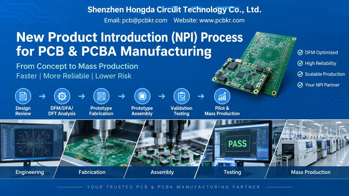
A mature PCB NPI process typically includes design review, design-for-manufacturing analysis, prototype fabrication, prototype assembly, several rounds of validation testing, and a controlled ramp into pilot and mass production. Skipping or rushing any of these stages is the single most common reason new products arrive late, fail certification, or generate high field-return rates in their first year.
The Complete NPI Process Flow: From Concept to Mass Production
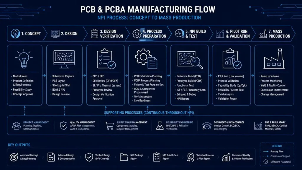
PCB & PCBA Manufacturing Flow: NPI Process from Concept to Mass Production
At Shenzhen Hongda Circuit Technology, our NPI workflow follows a linear, gated flow. Each gate requires sign-off before the board moves forward, which prevents defects from compounding downstream — a lesson the industry learned the hard way over decades of costly re-spins.
Product Concept and Requirement Definition
Every NPI process starts with defining electrical, mechanical, thermal, and regulatory requirements — impedance targets, layer count, copper weight, IPC class (Class 1, 2, or 3 per IPC-6012), and end-use environment. Locking these requirements early prevents the most expensive category of change: a spec change discovered after tooling is cut.
PCB Design Stage
The schematic is translated into a physical layout, with stack-up, trace routing, and via structures chosen to meet the requirement set. This is also where controlled-impedance planning and thermal relief design happen, both of which have outsized influence on first-pass yield later.
NPI Engineering Review
Before any material is cut, our engineering team reviews the design package — Gerbers, drill files, BOM, and assembly drawings — against fabrication and assembly capability. This is a manual, experience-driven checkpoint, not just a software rule-check, because automated DRC tools routinely miss issues like marginal annular ring on buried vias or BOM parts nearing end-of-life.
DFM / DFA / DFT Analysis
This is the stage where most manufacturability risk gets caught or missed. Design for Manufacturing (DFM) looks at whether the fab house can reliably produce the board — trace/space limits, aspect ratio on drilled holes, solder mask registration tolerance. Design for Assembly (DFA) checks component placement, package selection, and panelization for SMT line compatibility. Design for Test (DFT) verifies there is adequate test-point access for flying-probe or in-circuit test coverage. In our experience, roughly a third of first-time designs submitted for NPI carry at least one DFM issue serious enough to require a layout revision before fabrication.
PCB Prototype Fabrication
Bare boards are fabricated to the finalized design. Prototype runs are usually small (often single-digit to low double-digit panel counts) and are inspected far more intensively than a production lot — full electrical test, cross-sectioning on sample coupons, and dimensional verification against the IPC-A-600 acceptability standard.
PCBA Prototype Assembly
Components are placed and reflowed onto the bare board to build the first working assemblies. This stage validates not just the design but the assembly process itself — solder paste stencil design, reflow profile, and placement accuracy for fine-pitch or BGA components.
EVT (Engineering Validation Test)
Engineering Validation Test confirms the design meets its core electrical and functional specifications. This is where firmware bring-up, power-on testing, and initial functional debugging happen. EVT failures are expected and normal — this stage exists specifically to surface them cheaply, before tooling and process are locked further downstream.
DVT (Design Validation Test)
Design Validation Test verifies the product against its full requirement set under realistic conditions — thermal cycling, vibration, EMC pre-compliance, and mechanical fit. DVT units are typically built using production-intent tooling and processes so results reflect what customers will actually receive.
PVT (Production Validation Test)
Production Validation Test builds units on the actual production line, using production tooling, fixtures, and operators, at a build volume large enough to expose process variation that small prototype batches cannot reveal. A successful PVT run is usually the formal gate to release the product for pilot production.
Pilot Production
A limited production run under normal manufacturing conditions, used to validate yield rates, cycle time, and quality metrics at a scale close to full volume. Pilot data is what feeds the final capacity and yield planning for mass production.
Production Release
All engineering documentation — BOM, assembly drawings, test procedures, and quality specifications — is formally released and locked as the controlled baseline for manufacturing. From this point, any change requires a formal engineering change order (ECO).
Mass Production
The product moves into full-volume, ongoing manufacturing, monitored against the yield and quality baselines established during pilot production.
How Advanced Manufacturing Technology Shapes the NPI Process
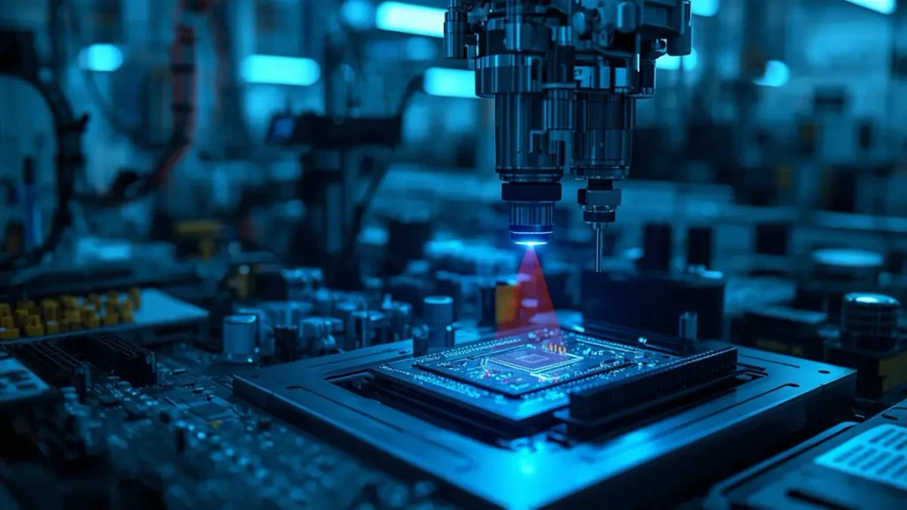
Advanced PCB Inspection and Manufacturing Technology
The equipment behind a fabrication and assembly line has a direct, measurable effect on how smoothly a design moves through NPI — and how tight the final tolerances can be held.
Laser Direct Imaging (LDI) replaces traditional photo-tooling with direct laser exposure of the resist layer, which improves line-width accuracy and layer-to-layer registration. This matters most during the PCB design and prototype fabrication stages, where tighter trace/space capability lets designers hit smaller feature sizes without needing a DFM-driven layout revision.
Automated Optical Inspection (AOI) at both the bare-board and post-assembly stages catches shorts, opens, and placement defects that are easy to miss visually, especially on high-density boards. Running AOI at the prototype stage, not just in mass production, is one of the highest-leverage habits an NPI process can adopt — it turns a defect that would otherwise surface during EVT debugging into a same-day fabrication finding.
X-ray inspection is essential for verifying solder joint quality on BGA, QFN, and other bottom-terminated components where the joint is not visible for optical inspection. During PCBA prototype and EVT stages, X-ray is often the only way to distinguish a design-related failure from an assembly-related one.
Flying probe testing allows electrical verification of prototype and low-volume boards without the cost and lead time of a dedicated bed-of-nails fixture, which is why it is the default test method during the earlier NPI stages, before test fixtures are built for production volume.
Impedance and TDR (time-domain reflectometry) testing confirms that controlled-impedance traces meet their target values on actual fabricated coupons, not just simulation — critical for high-speed digital and RF designs entering DVT.
Manufacturers that combine these capabilities in-house, rather than outsourcing steps across multiple vendors, generally compress NPI cycle time because engineering feedback from fabrication and assembly reaches the design team in days rather than weeks.
The Biggest Pain Points in Manufacturing During the NPI Process
Circuit Board Production Quality Control and Data Analysis
Across programs, the same handful of pain points recur more than any others:
DFM issues found too late. When manufacturability problems surface at PCBA prototype or EVT rather than during the DFM review, the cost of the fix multiplies — a layout change after tooling and stencils exist is far more expensive than the same change on paper.
BOM component availability. Parts specified during the design stage can go end-of-life or into allocation shortage by the time PVT or pilot production begins, forcing late substitutions that require re-qualification.
Inconsistent first-pass yield between prototype and pilot builds. A board that assembles cleanly at low volume with hand-tuned reflow settings can show yield drop-off once it moves to a production-representative line speed — usually a sign that DFA wasn’t fully validated at prototype scale.
Test coverage gaps. Boards designed without adequate test-point access for flying probe or ICT create blind spots in fault detection that aren’t discovered until failures show up in the field.
Documentation drift. When engineering changes made during EVT/DVT debugging aren’t formally captured before production release, the released BOM and drawings no longer match what was actually validated — a quiet but serious quality risk.
The common thread across all of these is timing: catching a problem one stage earlier in the NPI process is consistently cheaper than catching it one stage later.
Why an Experienced NPI Manufacturing Partner Matters
Standards and equipment set the baseline, but NPI success depends heavily on engineering judgment applied at each gate — knowing which DFM flags are cosmetic and which are genuine risk, and knowing when a marginal EVT result warrants a design hold rather than a workaround.
Our fabrication and assembly processes are built around recognized industry references, including IPC-6012 (qualification and performance of rigid PCBs), IPC-A-600 (acceptability of printed boards), J-STD-001 (requirements for soldered electrical and electronic assemblies), and IPC-A-610 (acceptability of electronic assemblies), alongside ISO 9001 quality management practices. These standards give customers a common, auditable language for what “acceptable” means at every NPI gate, rather than relying on informal or vendor-specific judgment calls.
Frequently Asked Questions
What Does NPI Mean in Engineering?
In engineering, NPI (New Product Introduction) refers to the structured process of taking a product from design concept through prototyping, validation testing, and pilot builds to a fully released, manufacturable design. It is an engineering discipline focused on de-risking a design before it reaches volume production.
What Does NPI Mean in Supply Chain?
In a supply chain context, NPI refers to the cross-functional coordination needed to launch a new product — sourcing components, qualifying suppliers, planning tooling and capacity, and managing the transition from prototype-quantity purchasing to production-volume purchasing without creating shortages or excess inventory.
What Is NPI Manufacturing?
NPI manufacturing is the fabrication and assembly work performed specifically to support the New Product Introduction process — building prototype, EVT, DVT, and PVT units under increasingly production-representative conditions, rather than standard high-volume production runs.
How Long Does the PCB NPI Process Typically Take?
Timelines vary with design complexity, but a typical NPI process spans several weeks to a few months from finalized design to production release, with prototype fabrication and assembly turnaround, validation test cycles, and any required design iterations as the main drivers of schedule.
What Documents Are Required to Start an NPI Process?
At minimum: finalized Gerber/ODB++ fabrication files, drill files, a complete BOM with approved manufacturer part numbers, assembly drawings, and any applicable test or acceptance specifications (e.g., target IPC class).
About the author
David Chen https://www.linkedin.com/in/pcbcoming
This article was prepared by a manufacturing engineer with over ten years of direct experience managing PCB and PCBA NPI programs, from DFM review through mass production ramp, across consumer, industrial, and communications electronics.
Shenzhen Hongda Circuit Technology Co., Ltd. supports customers through the full NPI process — from PCB design review and DFM/DFA/DFT analysis through prototype fabrication, PCBA assembly, and validation testing into mass production. Learn more at www.pcbkr.com. Email:pcb@pcbkr.com