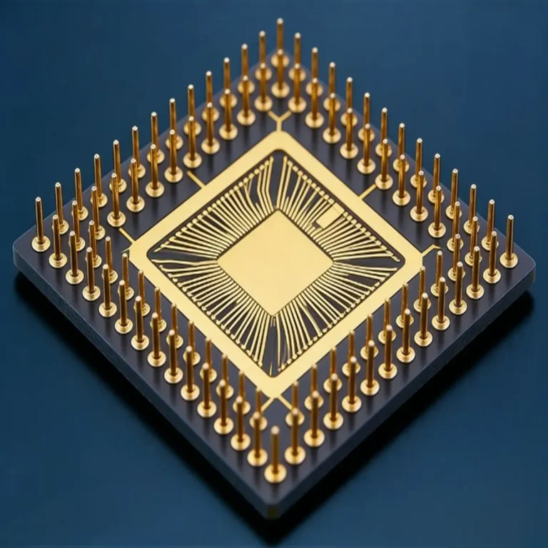
What Causes Tombstoning in SMT Assembly and How Can It Be Prevented?
Tombstoning defect cause mainly lies in unbalanced forces on two solder joints during SMT reflow, lifting one terminal of the SMD from PCB pads. Trigger factors include pad design, copper balance, paste volume, placement offset, poor solderability and improper reflow. Hongda Circuit offers PCB & PCBA services with pre-production risk checks. Email sales@pcbkr.com for project review.
What Is a Tombstoning Defect in SMT Assembly?
Tombstoning is an SMT soldering defect in which a small surface-mount component stands vertically or at an angle instead of remaining flat on both solder pads. One termination remains soldered to the PCB while the opposite end lifts away from its pad.
The defect is also known as the Manhattan effect because the raised component can resemble a building standing upright.
It most frequently affects small two-terminal passive components, including:
- 0201 and 01005 chip resistors
- 0402 and 0603 ceramic capacitors
- Small inductors and other chip components
Smaller components are particularly sensitive because their low mass makes them easier to rotate or lift when the soldering forces at their two terminations become unequal.
A tombstoned component can create an open circuit, interrupt a signal or power path, and cause functional test failures. Even when the defect is detected during inspection, repair adds labor, increases production cost, and may introduce additional thermal stress to the PCB and nearby components.
For procurement teams, tombstoning should therefore be treated as a manufacturing process-control issue rather than simply a cosmetic soldering defect.
What Causes Tombstoning During Reflow Soldering?
The fundamental mechanism behind tombstoning is an imbalance in the forces generated as solder melts and wets the component terminations and PCB pads.
During reflow, solder paste on both pads passes through a sequence of heating, flux activation, melting, and wetting. If one solder joint develops a stronger or earlier wetting force than the other, the resulting force difference can rotate the component and lift one end.
However, the actual cause is not always the same. A component may tombstone because of a PCB design characteristic, a printing variation, a placement error, a component-related issue, or an unsuitable thermal process.
The following factors should be investigated separately.
1. Asymmetric PCB Pad Geometry and Copper Distribution
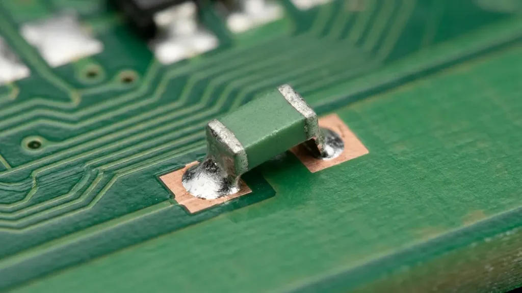
Tombstoning Caused by Asymmetric PCB Pad Geometry
PCB pad design is one of the first areas to investigate when tombstoning repeatedly occurs at the same component location.
Potential design-related causes include:
- Unequal pad dimensions or pad shapes
- Different copper connection areas on the two pads
- One pad connected directly to a large ground or power plane
- Inconsistent thermal relief connections
- Unequal local copper density
- Differences in nearby thermal mass
For example, one pad may connect directly to a large ground plane while the opposite pad connects to a relatively narrow signal trace. The larger copper area can change the local heat distribution during reflow.
As a result, the two pads may not reach the solder melting and wetting stages at the same rate.
This does not mean that every direct ground-plane connection causes tombstoning. The actual result depends on the PCB stackup, copper geometry, board thickness, component location, thermal conditions, and oven loading.
Recommended engineering checks:
- Review the PCB Gerber files and component land pattern.
- Compare the copper connections on both sides of the component.
- Check whether either pad is connected to a large copper region.
- Review thermal relief geometry and local copper density.
- Compare the suspected location with other positions where the same component is mounted.
If the defect consistently appears at one footprint or one board location, PCB design and local thermal conditions deserve particular attention.
2. Uneven Solder Paste Deposition
Solder paste volume and distribution directly affect the formation of the two solder joints.
When one pad receives significantly more solder paste than the other, the resulting solder joints may develop different wetting behavior during reflow. This can contribute to component rotation or lifting.
Common causes include:
- Unequal stencil aperture dimensions
- Inconsistent paste release from stencil openings
- Stencil blockage or contamination
- Printing misalignment
- Poor PCB support during printing
- Variations in solder paste condition
- Incorrect stencil thickness or aperture design
For small components, even relatively small differences in paste deposition can become significant.
How should engineers investigate the problem?
Compare the solder paste deposits on both pads of the affected component. Where solder paste inspection (SPI) data is available, review the measured volume, height, area, and positional offset rather than relying only on visual inspection.
The investigation should also compare:
- Affected component locations
- Similar components without defects
- Different PCB panels or production batches
- Printing conditions before and after the defect appeared
A useful distinction is whether the paste imbalance is isolated to one footprint or appears across many components. A repeated pattern may indicate a stencil or printing-process issue rather than an isolated PCB design problem.
3. Component Placement Offset and Rotation
Incorrect component placement can increase the likelihood of tombstoning.
If a chip component is placed too far from the center of its footprint, the two terminations may not initially contact their solder paste deposits in the intended positions.
Potential contributing factors include:
- Incorrect component center coordinates
- Excessive placement offset
- Component rotation errors
- Incorrect nozzle selection
- Inconsistent pickup or release
- Unsuitable placement pressure
- Feeder or vision-recognition errors
Placement offset alone does not prove the root cause. It should be assessed together with solder paste distribution and the final solder joint geometry.
Recommended checks include:
- Review the placement program and component coordinates.
- Compare actual component positions with the PCB footprint.
- Check placement accuracy for the affected package size.
- Inspect nozzle condition and component pickup consistency.
- Compare the affected components with correctly assembled examples.
If the defect occurs across several component types or board locations, the placement process should be reviewed as part of a wider process investigation.
4. Component Termination Oxidation and Poor Solderability
The condition of component terminations can also affect solder wetting.
Oxidation, contamination, damaged plating, or inconsistent termination quality may prevent one end of a component from wetting properly.
Potential sources include:
- Component storage conditions
- Moisture or contamination exposure
- Oxidized or damaged terminations
- Differences between component manufacturing lots
- Inconsistent solderability of incoming components
A component-related problem may become more apparent when a new material lot is introduced.
When tombstoning starts after a component supplier or batch change, engineers should compare the affected and unaffected lots instead of immediately modifying the reflow profile.
Incoming material records, component packaging condition, termination appearance, and supplier quality information can help establish whether the issue is batch-related.
5. Unsuitable Reflow Temperature Profile
Reflow conditions influence how quickly solder paste heats, activates, melts, and wets the component terminations.
An unsuitable temperature profile may increase the difference between the thermal response of the two pads.
Relevant process variables include:
- Heating ramp rate
- Preheat and soak conditions
- Time above liquidus
- Peak temperature
- Board-level temperature variation
- Conveyor speed
- PCB loading and orientation
A key point is that the temperature displayed by the reflow oven does not necessarily represent the temperature experienced by every component on the PCB.
A board with large copper areas, different component thermal masses, and uneven component distribution may experience different thermal responses across its surface.
Do not assume that increasing or decreasing the oven temperature will automatically solve tombstoning.
A suitable investigation should measure the actual temperature profile on representative PCB locations using thermocouples. The measured profile should then be compared with the solder paste manufacturer’s process requirements and the assembly’s thermal limitations.
Any adjustment should also be checked for its effect on other components and solder joints.
How Should Engineers Diagnose a Tombstoning Defect?
Effective root cause analysis requires more than identifying the possible causes. Engineers need to determine which factor is responsible for the actual production defect.
A practical investigation should follow a structured sequence.
Step 1: Identify the Defect Distribution
Start by recording where tombstoning occurs.
Check whether the affected components share:
- The same PCB reference designator
- The same component package
- The same board location
- The same lifting direction
- The same PCB panel position
- The same component or solder paste lot
- The same production date or SMT line
If the defect repeatedly occurs at the same component location, investigate the footprint, copper distribution, and local thermal environment.
If multiple unrelated components are affected, a common process factor may be involved.
Step 2: Review Solder Paste Printing Evidence
Inspect the two solder paste deposits associated with each affected component.
Where SPI records are available, compare:
| Inspection parameter | What engineers should investigate |
|---|---|
| Paste volume | Difference between the two pads |
| Paste height | Uneven deposit height |
| Paste area | Inconsistent stencil transfer |
| Printing offset | Paste displaced from the pad center |
| Repeated variation | Similar imbalance across multiple boards |
The purpose is to determine whether the solder paste deposits were already unbalanced before component placement and reflow.
Step 3: Check Component Placement Records
Review the actual placement position and orientation of affected components.
Compare the placement data with the original PCB coordinates and examine whether the same offset appears on multiple boards.
If the component is consistently misplaced, investigate the placement program, vision recognition, nozzle condition, and machine setup.
Step 4: Review Gerber Data and PCB Thermal Characteristics

PCB Gerber and Copper Distribution Analysis
For recurring defects at specific locations, review the PCB design.
The investigation should include:
- Pad dimensions and spacing
- Copper connection geometry
- Ground and power plane connections
- Local copper density
- Thermal relief design
- Nearby large copper areas
- Component spacing and surrounding thermal mass
The objective is to identify whether the two pads experience significantly different thermal conditions during reflow.
Step 5: Compare Component Lots and Solderability
If the defect is associated with a specific component batch, review the incoming material records.
Check component termination condition, packaging, storage, and supplier quality documentation.
Where necessary, conduct suitable solderability evaluation or supplier investigation rather than assuming that the PCB design is responsible.
Step 6: Measure the Actual Reflow Profile
Use representative PCB assemblies and thermocouple measurements to assess the temperature profile at relevant locations.
Compare the measured results against:
- The solder paste manufacturer’s recommended profile
- Component temperature limitations
- PCB thermal characteristics
- Actual production loading conditions
The purpose is to determine whether the affected components experience a different thermal response from other board locations.
Step 7: Confirm the Root Cause Through Controlled Trials
A suspected cause should be tested before implementing a permanent process change.
For example:
- If copper imbalance is suspected, compare affected and alternative footprint configurations where design changes are feasible.
- If printing variation is suspected, evaluate stencil cleaning, aperture design, and printing conditions.
- If placement offset is suspected, verify the result after controlled machine adjustment.
- If reflow is suspected, compare measured profiles under controlled loading conditions.
A root cause should be considered confirmed only when the evidence supports the explanation and the corrective action produces a repeatable improvement.
What Corrective Actions Can Reduce Tombstoning?
Corrective actions should target the verified cause. Applying several unrelated process changes at once makes it difficult to determine which adjustment actually improved the result.
| Verified problem | Corrective action direction | Validation method |
|---|---|---|
| Unequal pad geometry | Review and correct land pattern dimensions | Compare revised footprint and assembly results |
| Asymmetric copper connection | Evaluate copper balance and thermal relief | Review Gerber and test representative assemblies |
| Uneven paste deposition | Optimize stencil aperture, cleaning, and printing conditions | Compare SPI measurements |
| Placement offset | Correct placement coordinates and machine setup | Verify component position and orientation |
| Poor component solderability | Investigate incoming material and supplier lot | Compare lot records and solderability results |
| Uneven thermal response | Optimize the reflow profile based on measured board temperatures | Compare thermocouple profiles and solder joint results |
| Process variation between batches | Improve process monitoring and material traceability | Review production trends and recurrence data |
Why Changing the Reflow Profile Alone May Not Solve Tombstoning
Adjusting the reflow profile is a common response to soldering defects, but it should not be the first and only corrective action.
Consider three different production situations:
Situation 1: Tombstoning occurs at one specific footprint.
The two pads may have different copper connections or local thermal characteristics. Changing the entire oven profile could affect the rest of the PCB without correcting the underlying design issue.
Situation 2: Tombstoning occurs across multiple component locations.
A common printing, placement, or reflow condition may be involved. Process records should be reviewed to identify the shared factor.
Situation 3: Tombstoning appears after a component lot change.
The component terminations, storage conditions, or incoming material quality should be investigated before making broad changes to the assembly process.
The correct approach is to identify the mechanism first and then select the smallest effective corrective action.
How Can PCBA Manufacturers Prevent Tombstoning in Mass Production?
Preventing tombstoning in mass production requires controls at several stages, from design review to final inspection.
1. Conduct DFM and DFA Reviews Before Production
The PCB and assembly data should be reviewed before the first production run.
Important checks include:
- Small passive component footprints
- Pad symmetry and solder mask definition
- Copper connections and thermal relief
- Component spacing
- Stencil aperture requirements
- Placement accessibility
- Potential local thermal imbalances
Early engineering review can identify potential assembly risks before they become repeated production defects.
PCBKR provides engineering support for PCB fabrication and PCBA assembly projects. Customers can submit Gerber files, BOM information, and assembly requirements for project evaluation.
For broader design-stage considerations, see our PCB DFM engineering review.
2. Control Solder Paste Printing
Solder paste printing should be controlled through appropriate stencil design, printing parameters, cleaning frequency, and inspection.
Where SPI is available, inspection data can help identify abnormal paste volume or positional variation before reflow.
The objective is not simply to detect printing defects but to prevent inconsistent solder paste deposits from reaching the next production stage.
3. Verify Component Placement Accuracy
Placement programs should be validated against the actual PCB design and component specifications.
Small passive components require particular attention because placement errors can influence their initial position relative to the solder paste deposits.
Machine setup, feeder condition, nozzle selection, and vision recognition should be maintained according to the production requirements.
4. Validate Reflow Conditions With Actual PCB Assemblies
Reflow conditions should be established using representative assemblies rather than relying only on standard oven settings.
Validation should consider:
- PCB thickness and copper distribution
- Component thermal mass
- Board loading
- Solder paste requirements
- Component temperature limitations
- Temperature differences between board locations
This is especially important for multilayer boards, high-copper designs, and assemblies with mixed component sizes.
5. Use Inspection and Electrical Testing to Identify Assembly Problems
Visual inspection and automated optical inspection (AOI) can help identify tombstoned components and other visible assembly defects.
For assemblies with hidden solder joints or fine-pitch packages, X-ray inspection may provide additional evidence where applicable.
Electrical testing can help determine whether the assembly meets the specified functional or connectivity requirements.
The inspection method should match the package type, defect risk, and customer acceptance requirements. AOI alone should not be treated as proof that every solder joint is reliable.
6. Monitor Production Trends and Prevent Recurrence
A single corrected board does not demonstrate that a manufacturing problem has been permanently resolved.
Manufacturers should review defect trends across production batches and retain relevant process information.
A practical quality-control system should include:
- Defect records by component reference and package
- Material and component lot traceability
- Inspection and test results
- Reflow profile records where required
- Corrective action documentation
- Process change review
- Verification of subsequent production batches
This creates a feedback loop between engineering, production, and quality teams.
For customers evaluating a new PCBA manufacturing partner, our PCB Assembly Services Buyer’s Guide explains additional factors to consider when assessing supplier capabilities.
How Should Buyers Evaluate a PCBA Supplier’s Tombstoning Control?
For overseas OEMs and electronics manufacturers, the supplier’s response to a soldering defect is often more important than a simple statement that the factory has AOI equipment.
A capable PCBA supplier should be able to explain how it identifies the defect, investigates its cause, implements corrective actions, and verifies the result.
Before selecting a supplier, buyers should ask the following questions.
Can the Supplier Identify the Actual Root Cause?
Ask whether the engineering team can review PCB Gerber data, component footprints, solder paste conditions, placement records, and reflow parameters.
A supplier that immediately recommends changing the oven temperature without examining the other process variables may not have completed a sufficient root cause investigation.
Can the Supplier Provide Inspection and Process Evidence?
Depending on the project requirements, ask whether the supplier can provide relevant records such as:
- Visual inspection and AOI results
- X-ray inspection results where applicable
- Solder paste inspection records where available
- Reflow temperature profile data
- Electrical test results
- Defect and corrective action reports
The availability and scope of these records should be agreed upon during project review.
Can the Supplier Support Both PCB Fabrication and PCBA Assembly?
Tombstoning can involve both PCB design and assembly-process factors.
When the same supplier handles PCB fabrication and PCBA assembly, engineering teams can coordinate the review of pad geometry, copper distribution, material selection, and assembly conditions.
This does not automatically eliminate defects, but it can simplify technical communication and shorten the feedback loop between PCB design review and assembly production.
Can the Supplier Support Prototype, Pilot, and Mass Production?
A process that works on a few prototype boards may not remain stable when production volume increases.
Buyers should evaluate whether the supplier can support:
- Prototype and sample production
- First-article inspection
- Pilot production validation
- Repeat production
- Material and process traceability
- Corrective action and process change management
For NPI-related engineering support, see our NPI Engineering for PCB and PCBA service information.
PCBKR PCB and PCBA Manufacturing Support
Hongda Circuit provides PCB fabrication and PCBA assembly services for customers developing and manufacturing electronic products.
For projects involving small passive components, high-density layouts, or demanding assembly requirements, engineering review should consider both PCB design characteristics and downstream SMT process conditions.
Depending on the project scope and customer specifications, PCBKR can support:
- PCB fabrication based on customer Gerber and technical requirements
- PCBA assembly based on customer BOM and assembly documentation
- DFM and assembly-risk review
- Inspection and quality-control planning
- AOI and X-ray inspection where applicable
- Electrical testing according to project requirements
- Prototype, small-batch, and mass-production manufacturing
Actual manufacturing parameters, inspection scope, testing methods, and acceptance criteria should be confirmed against the customer’s drawings, BOM, specifications, and quality requirements.
If your current supplier is experiencing repeated tombstoning, or you are qualifying a new PCBA manufacturing partner, PCBKR can review the project information and discuss suitable manufacturing controls.
Request a PCB/PCBA Manufacturing Review
Send the following information for an initial project evaluation:
- PCB Gerber files
- BOM and component package information
- Assembly drawings or placement files
- Photos of the tombstoning defects, if available
- Production quantity and delivery requirements
- Applicable quality and inspection specifications
Contact Hongda Circuit
Email: sales@pcbkr.com
Website: https://www.pcbkr.com/
Shenzhen Hongda Circuit Technology Co., Ltd.
PCB Fabrication | PCBA Assembly | Prototype to Mass Production
Frequently Asked Questions About Tombstoning Defects
What is the most common cause of tombstoning in SMT assembly?
Tombstoning is caused by an imbalance in the forces generated by molten solder at the two ends of a surface-mount component. Uneven pad heating, asymmetric copper connections, unequal solder paste deposits, and placement variation can contribute to this imbalance. The dominant cause must be confirmed through inspection and process evidence.
Can a PCB assembly manufacturer prevent tombstoning on 0201 and 01005 components?
A manufacturer can reduce the risk through appropriate PCB footprint review, stencil design, solder paste control, placement verification, reflow validation, and production inspection. However, no responsible supplier should guarantee that tombstoning can never occur under every design and production condition. The process should be evaluated against the actual component, PCB, materials, and customer requirements.
How do I know whether tombstoning is caused by PCB design or the SMT process?
Start by comparing the defect distribution across component locations, PCB panels, and production batches. Repeated defects at the same footprint may indicate a design or local thermal issue. Defects across unrelated locations may point toward printing, placement, material, or reflow conditions. Gerber review, solder paste inspection records, placement data, and actual reflow profiles help distinguish the causes.
What information should I send to a PCBA supplier for tombstoning troubleshooting?
Provide PCB Gerber files, BOM, component package details, assembly drawings, defect photos, production quantity, and any available inspection or process records. If the issue has occurred during production, include the affected component reference designators, production batch, and information about recent material or process changes. This allows the supplier’s engineering team to investigate the problem more efficiently.
What should buyers check before choosing a PCB assembly supplier for high-reliability products?
Buyers should evaluate the supplier’s PCB and PCBA engineering support, SMT process control, inspection capability, electrical testing scope, traceability, and corrective action process. Ask for evidence of how the supplier investigates defects and verifies improvements across production batches. The supplier should also confirm that its manufacturing and inspection capabilities match the product’s technical specifications and required quality standards.
About Author
David Chen LinkedIn Profile
David Chen is a Senior RF/PCB Process Engineer at Shenzhen Hongda Circuit Technology Co., Ltd., with over 12 years of experience in high-frequency PCB fabrication, impedance-controlled stack-up design, and Rogers/PTFE laminate processing. He also boasts an extensive professional background in PCBA manufacturing, PCBA testing, and PCBA optimization, with specialized expertise in high-precision PCBA fault analysis and rigorous PCBA reliability testing. The author has worked with high-layer-count server PCB fabrication, ultra-low-loss backplane stackups, and thermo-mechanical reliability optimization for AI infrastructure projects involving 112G and 224G PAM4 architectures. Skilled in complex circuit design and cutting-edge advanced PCB manufacturing processes, he delivers solutions that elevate product durability and performance across industrial applications. His technical articles focusing on PCBA manufacturing workflows and testing methodologies are widely cited by industry peers and technical platforms, and have gained attention and recognition from industry colleagues.