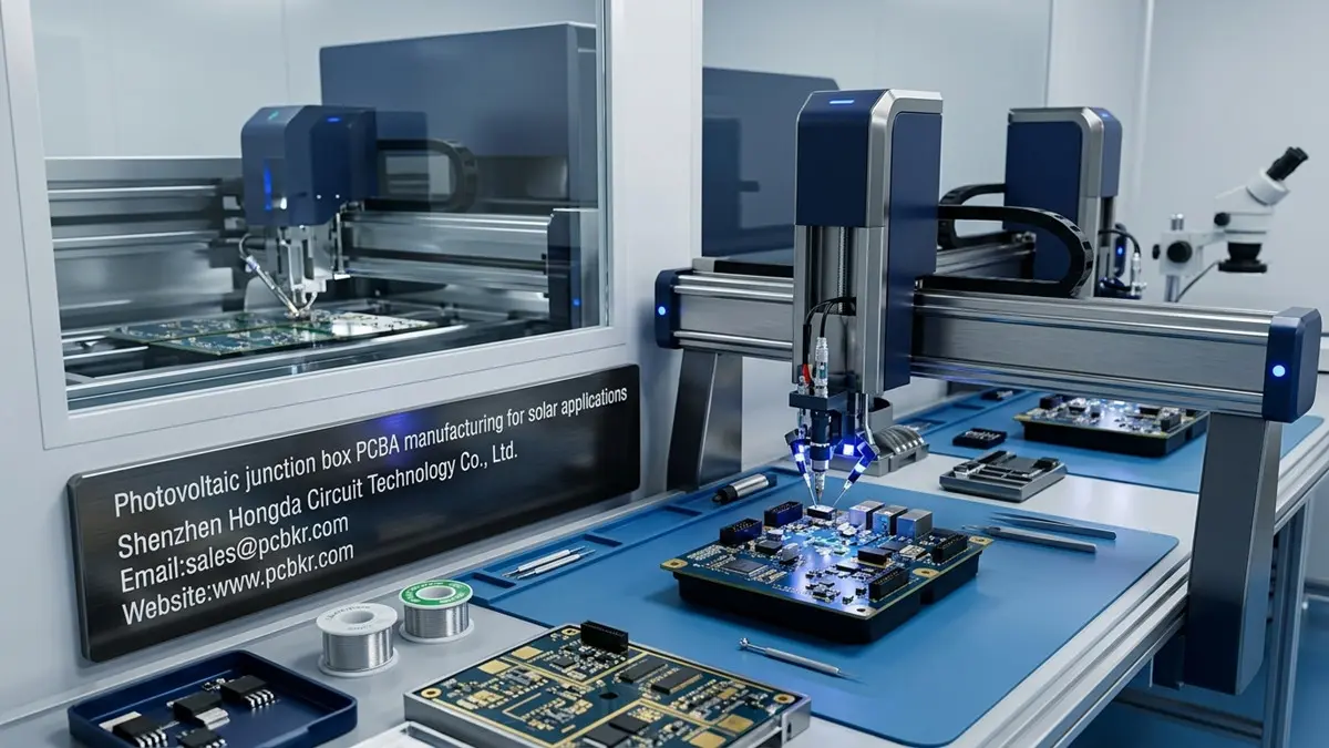
Photovoltaic Junction Box PCBA Manufacturing for Solar Applications
Photovoltaic junction box PCBA manufacturing requires more than assembling electronic components onto a printed circuit board. The PCB must meet the customer’s electrical, thermal, insulation, and mechanical requirements while maintaining consistent manufacturing quality. Shenzhen Hongda Circuit Technology Co., Ltd. (PCBKR) provides PCB fabrication and PCBA assembly for photovoltaic junction box applications, backed by actual production experience in this product category.
PCBKR supports OEM customers with custom PCB manufacturing and electronic assembly based on customer-provided Gerber files, BOMs, assembly drawings, and technical specifications. From engineering review and PCB fabrication to SMT/THT assembly and quality inspection, our manufacturing service helps photovoltaic equipment manufacturers source their internal PCB assemblies through one manufacturing partner.
For photovoltaic junction box manufacturers and solar module OEMs, PCBKR provides a practical manufacturing solution for prototype evaluation, small-batch production, and volume manufacturing, subject to project requirements and production assessment.
Photovoltaic Junction Box PCB and PCBA Manufacturing
A photovoltaic junction box is installed on a solar module to provide electrical connections and protection for the module’s internal circuits. Depending on the product architecture, the junction box may contain bypass diodes, conductive connections, or additional electronic circuits for converting, controlling, or monitoring functions.
When a junction box design includes a printed circuit board or electronic assembly, the PCB becomes an important part of the product’s electrical and mechanical integration.
PCBKR manufactures and assembles internal PCBs and PCB assemblies for photovoltaic junction box applications. Our confirmed service scope covers:
- PCB fabrication: Manufacturing printed circuit boards according to customer-approved Gerber data, stack-up requirements, materials, copper specifications, and dimensional tolerances.
- PCBA assembly: SMT and THT component assembly according to the approved BOM, assembly drawings, component specifications, and production instructions.
- OEM manufacturing: Production based on customer designs and technical documentation, with project requirements reviewed before manufacturing.
- Production inspection: PCB and assembly inspection using applicable manufacturing quality-control processes.
- Production support: Manufacturing support for prototype, small-batch, and volume requirements, subject to project review.
PCBKR has already produced photovoltaic junction box internal PCB/PCBA products. This practical production experience provides a manufacturing foundation for customers looking for a PCB and PCBA supplier familiar with this application.
The exact production scope depends on the customer’s product architecture. PCB fabrication and PCBA assembly should not be confused with manufacturing the complete junction box, including its enclosure, cables, connectors, terminals, busbars, sealing, or other mechanical and electrical components.
PCB Requirements for Photovoltaic Junction Box Applications
The PCB requirements for a photovoltaic junction box depend on its electrical function, component selection, operating environment, and mechanical structure. A board carrying power-related components may have different requirements from a low-power monitoring or control board.
A manufacturing review should consider the following design factors before production.
PCB Structure and Material Selection
The PCB material and stack-up should be selected according to the electrical, thermal, mechanical, and environmental requirements of the application.
Important parameters include:
- PCB material and applicable material grade
- Number of copper layers
- Finished board thickness
- Copper thickness for each relevant layer
- Minimum trace width and spacing
- Finished hole diameter and via structure
- Surface finish
- Board dimensions and dimensional tolerances
- Solder mask and legend requirements
Material selection should not be based on a generic solar PCB specification. The correct material depends on the actual design, operating temperature, insulation requirements, component power dissipation, and customer qualification criteria.
PCBKR reviews the customer’s PCB data and manufacturing requirements before confirming the production process and quotation.
Component Layout and Manufacturing Considerations
Photovoltaic junction box PCBA designs may have limited installation space. Component placement, pad geometry, soldering access, and board dimensions therefore need to be considered together.
During manufacturing preparation, the following items should be reviewed:
- Component package compatibility with the PCB footprint
- Polarity and orientation of diodes and other polarized components
- Pad dimensions and soldering requirements
- Component spacing and assembly accessibility
- Potential interference with the customer’s enclosure or mechanical structure
- Special process requirements for power components
The PCB layout and assembly drawing should be consistent. Differences between the Gerber files, BOM, component datasheets, and assembly documentation should be resolved before production.
Bypass Diode Integration and PCB Thermal Management
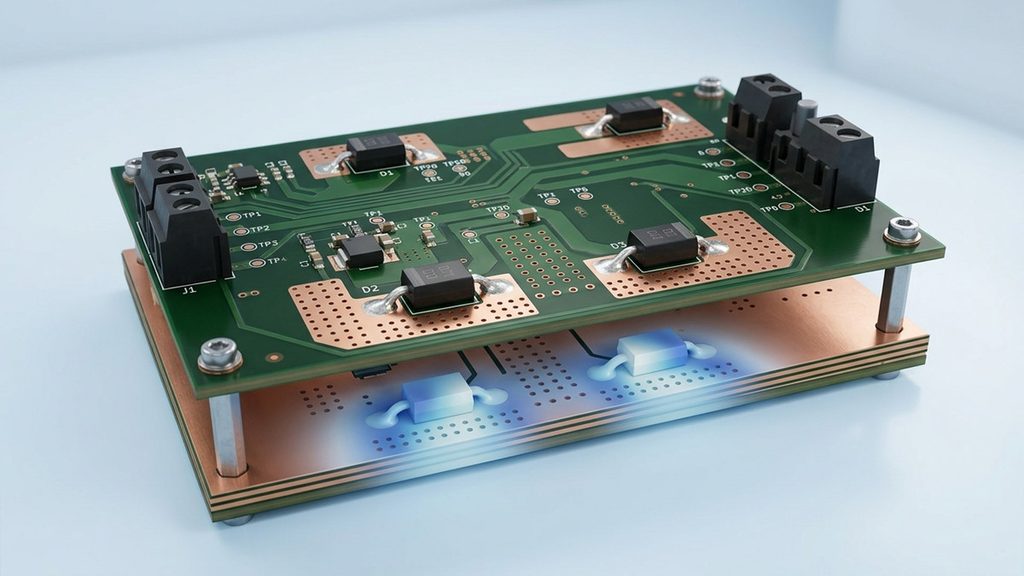
Photovoltaic Junction Box PCBA Bypass Diode Thermal Management
Bypass diodes are used in photovoltaic module junction box designs to provide an alternative current path under specified operating conditions. Their electrical and thermal behavior is important to the overall junction box design.
Where bypass diodes are mounted on or electrically connected through a PCB, the board layout and thermal path can influence operating temperature and long-term reliability.
Heat Dissipation Around Bypass Diodes
A bypass diode dissipates power during operation. The amount of heat depends on the device characteristics and actual operating conditions, including current and forward voltage.
The PCB design review may need to consider:
- Copper area around the diode pads
- Copper thickness and current path
- Thermal spreading through copper layers
- Thermal vias, where included in the design
- Distance between heat-generating components
- Thermal coupling to the enclosure or other heat-dissipation structures
- Local temperature rise under the specified operating conditions
A larger copper area or additional thermal vias may help spread heat, but neither guarantees acceptable junction temperature by itself. The complete thermal path, component package, solder interface, PCB construction, enclosure design, and operating environment all influence the result.
PCB manufacturers should therefore work from the customer’s approved design and applicable thermal requirements rather than selecting copper thickness or thermal-via quantities based on an assumed current rating.
PCB and Solder Joint Reliability
Thermal cycling can cause repeated expansion and contraction of PCB materials, components, and solder joints. Differences in material properties and local temperature gradients may contribute to mechanical stress.
For photovoltaic junction box PCBA, the manufacturing review should pay attention to:
- Solder joint formation and consistency
- Component termination and pad design
- PCB surface finish compatibility
- Soldering process requirements
- Component placement and alignment
- Inspection criteria for power-device connections
The customer’s design qualification and reliability testing should define the required operating limits. PCBA manufacturing inspection can verify assembly quality, but it cannot replace complete product-level thermal and reliability validation.
High-Current PCB Design and Electrical Connections
Some photovoltaic junction box designs contain power-related electrical paths. These designs may require careful coordination between copper thickness, conductor geometry, component terminals, and the external connection structure.
A high-current PCB should not be specified by copper weight alone.
Copper Thickness and Current-Carrying Capacity
The current-carrying capability of a PCB trace depends on several interacting factors:
- Trace width and copper thickness
- Internal or external copper-layer location
- Permitted temperature rise
- Ambient temperature
- PCB material and thermal properties
- Nearby heat-generating components
- Cooling conditions and enclosure design
- Duration and profile of the operating current
The required copper specification should be confirmed against the customer’s electrical design and thermal calculations.
For designs requiring heavier copper, PCBKR can review the specified copper requirements as part of its PCB fabrication assessment. Related manufacturing information is available on our Heavy Copper PCB manufacturing page.
Electrical Connection and Soldering Considerations
The interface between PCB pads, component leads, and other conductive structures can affect electrical and mechanical reliability.
Manufacturing documentation should define:
- Pad and hole dimensions
- Component termination requirements
- Solder alloy and soldering process requirements, where specified
- Acceptable solder joint appearance
- Electrical test requirements
- Any special inspection criteria
The design of terminals, busbars, cables, and external conductive connections remains dependent on the complete junction box architecture. PCBKR’s confirmed service scope is the internal PCB fabrication and PCBA assembly, not automatic manufacturing of all junction box conductive or mechanical components.
Insulation and Environmental Reliability Requirements
Photovoltaic junction boxes operate as part of outdoor solar modules. Their design must account for the intended electrical ratings and environmental conditions.
For PCB and PCBA manufacturing, insulation and environmental requirements should be communicated clearly during the engineering review.
Clearance and Creepage Distance
Clearance is the shortest distance through air between conductive parts. Creepage is the shortest distance along an insulating surface between conductive parts.
The required distances depend on the applicable design standard, working voltage, insulation category, pollution conditions, material properties, and other relevant factors.
The PCB layout should be reviewed against the customer’s approved insulation requirements. Relevant items may include:
- Spacing between conductive pads and tracks
- Distance between component terminals
- Solder mask limitations and exposed copper
- PCB material and surface conditions
- Slots or cut-outs specified in the design
- Component package insulation characteristics
Solder mask should not be treated as an automatic substitute for the required insulation distance.
Environmental and Thermal Conditions
The complete junction box may be exposed to moisture, temperature variation, ultraviolet radiation, and other outdoor conditions. These factors influence material selection and product qualification.
For the PCB assembly, the customer should define applicable requirements for:
- Operating and storage temperature
- Thermal cycling
- Moisture exposure
- Insulation resistance
- Dielectric withstand testing, where applicable
- Corrosion-related material requirements
- Environmental qualification of the complete assembly
The PCB/PCBA supplier should manufacture against the agreed drawings, material requirements, and acceptance criteria. Complete junction box environmental qualification remains a product-level responsibility defined by the OEM and its certification or testing program.
PCB Fabrication Process for Photovoltaic Junction Box Boards
Consistent PCB fabrication starts with reviewing the customer’s design data and confirming the manufacturing specifications.
PCBKR’s PCB manufacturing workflow is based on the approved production files and technical requirements.
1. Gerber and Engineering Data Review
The engineering review checks the supplied fabrication data and identifies missing or conflicting requirements.
Typical review items include:
- Gerber file completeness
- PCB outline and dimensions
- Layer definition and stack-up
- Copper thickness
- Drill data
- Surface finish
- Solder mask and legend
- Controlled tolerances
- Special manufacturing notes
Any unclear specification should be confirmed with the customer before production.
2. Material and Stack-Up Confirmation
The PCB material, copper construction, finished thickness, and layer arrangement are confirmed against the approved design.
For multilayer boards, stack-up details should be reviewed to ensure the manufacturing construction matches the customer’s requirements.
3. PCB Fabrication
The fabrication process follows the confirmed PCB construction and manufacturing instructions. Depending on the design, production may include imaging, etching, lamination, drilling, plating, solder mask application, surface finishing, and profiling.
The actual process route depends on the board structure and selected manufacturing specifications.
4. PCB Inspection
Finished boards are checked against applicable dimensional, visual, and electrical requirements.
Inspection items may include:
- Board dimensions and outline
- Surface condition
- Solder mask and surface finish
- Hole and via quality
- Copper pattern integrity
- Electrical continuity and isolation, as specified
The inspection scope should be agreed according to the customer’s drawings and quality requirements.
SMT and THT Assembly for Photovoltaic Junction Box PCBA
Photovoltaic junction box PCBA assembly requires accurate component placement and controlled soldering processes. The production requirements depend on the component packages, PCB design, and customer assembly specifications.
PCBKR provides SMT and THT assembly as part of its PCB and PCBA manufacturing services.
BOM and Component Review
Before assembly, the BOM should be checked for:
- Manufacturer part numbers
- Component package and footprint
- Electrical ratings
- Polarity
- Approved alternatives
- Availability and supply requirements
- Special handling or storage instructions
For power components such as diodes, the component datasheet and customer-approved part number should be used to confirm package, polarity, and assembly requirements.
SMT and THT Production
The assembly method depends on the component package and PCB design.
SMT components are placed on surface-mount pads and soldered according to the approved process. Through-hole components are installed and soldered according to the assembly drawing and applicable process requirements.
Important production controls include:
- Component placement accuracy
- Polarity and orientation
- Solder paste application
- Reflow profile requirements
- Through-hole soldering quality
- Component alignment
- PCB handling and protection
The process should be matched to the actual assembly design rather than assuming every photovoltaic junction box PCBA uses the same component configuration.
PCBA Quality Inspection and Electrical Testing
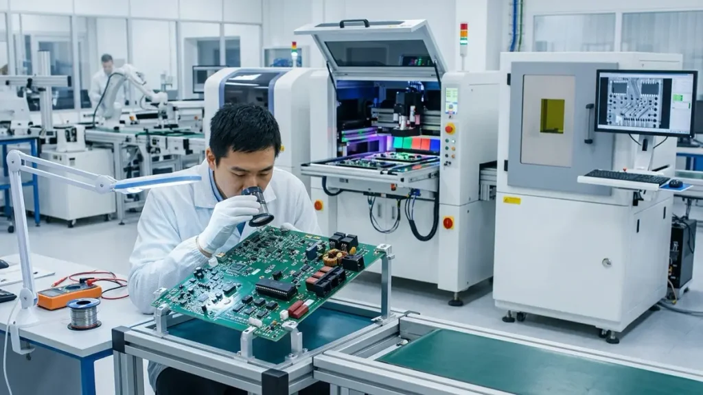
Photovoltaic Junction Box PCBA Quality Inspection and Electrical Testing
Quality inspection should verify that the assembled PCB conforms to the customer’s approved manufacturing and acceptance requirements.
PCBKR has manufacturing inspection capabilities including 3D AOI, X-ray inspection, and electrical testing equipment. The inspection methods selected for a photovoltaic junction box PCBA depend on the board design, component package, test coverage, and customer specifications.
Visual and Automated Inspection
Visual inspection and automated optical inspection can be used to check applicable assembly characteristics, such as:
- Component presence and placement
- Polarity and orientation
- Solder joint appearance
- Component alignment
- Visible assembly defects
X-ray inspection may be appropriate for solder joints that cannot be adequately evaluated by visual inspection, depending on the package and assembly structure.
Electrical Testing
Electrical testing should be defined according to the circuit design and customer test specification.
Depending on the product, the test plan may include continuity, isolation, resistance, or functional checks. Functional testing requires an agreed test method, fixture, test limits, and relevant operating conditions.
A manufacturing inspection report should distinguish between:
- PCB fabrication inspection
- PCBA assembly inspection
- Electrical testing
- Customer-specific functional testing
- Complete junction box qualification
These activities are not interchangeable. A PCBA inspection report does not, by itself, establish that the complete photovoltaic junction box complies with all applicable product standards.
OEM Photovoltaic Junction Box PCBA Procurement
For OEM buyers, the most efficient way to obtain an accurate quotation is to provide complete and consistent engineering documentation.
PCBKR evaluates photovoltaic junction box PCB and PCBA projects based on the customer’s actual design, production quantity, component requirements, and inspection specifications.
Documents Required for an RFQ
| Document or Information | Purpose |
|---|---|
| Gerber or ODB++ files | PCB fabrication assessment |
| PCB stack-up | Layer and material construction |
| BOM with manufacturer part numbers | Component and sourcing review |
| Assembly drawings | Component placement and orientation |
| Pick-and-place / centroid file | SMT assembly preparation, where applicable |
| Drill files | PCB hole and via manufacturing |
| PCB technical specification | Thickness, copper, finish, and tolerances |
| Test specification | Inspection and electrical test planning |
| Required quantity | Production planning and quotation |
| Target delivery date | Lead-time assessment |
If the customer has not finalized all documents, the available files can be submitted for an initial review. Missing information should be identified before the quotation and production scope are confirmed.
Factors Affecting Photovoltaic Junction Box PCBA Cost
The cost of a photovoltaic junction box PCBA depends on both PCB fabrication and electronic assembly requirements.
Major cost factors include:
- PCB size, layer count, material, and copper thickness.
- Finished board thickness and special manufacturing tolerances.
- Surface finish and required PCB specifications.
- BOM complexity and component package types.
- SMT and THT assembly quantities.
- Special soldering or handling requirements.
- Inspection coverage and electrical testing.
- Production quantity and material sourcing arrangements.
- Packaging, delivery, and project-specific requirements.
A reliable quotation should be based on the actual Gerber files, BOM, assembly drawings, quantity, and test requirements rather than a generic price per board.
Prototype, Small-Batch, and Volume Production
Photovoltaic OEM projects may require engineering samples before moving into regular production.
A typical manufacturing sequence includes:
- Review of PCB and PCBA documentation.
- Confirmation of material, components, and manufacturing scope.
- Prototype or sample production, where required.
- Customer inspection and design validation.
- Revision control and production approval.
- Small-batch or volume manufacturing.
The transition to volume production should use the approved PCB revision, BOM, assembly documentation, and quality acceptance criteria. Any design or component change should be reviewed before it is introduced into production.
Why Choose PCBKR for Photovoltaic Junction Box PCB and PCBA Manufacturing?
PCBKR provides PCB fabrication and PCBA assembly for OEM customers requiring a manufacturing partner for electronic circuit boards.
For photovoltaic junction box applications, our service is based on actual production experience and a defined focus on internal PCB and PCBA manufacturing.
Customers can work with PCBKR for:
- Relevant production experience: PCBKR has already manufactured and assembled internal PCB/PCBA products for photovoltaic junction box applications.
- PCB fabrication: Production according to customer Gerber files, stack-up, material, copper, and dimensional requirements.
- PCBA assembly: SMT and THT assembly according to the approved BOM and assembly documentation.
- Manufacturing inspection: Applicable visual, AOI, X-ray, and electrical inspection capabilities based on project requirements.
- OEM production support: Project evaluation for prototype, small-batch, and volume production.
- Engineering document review: Confirmation of manufacturing data, component information, and inspection requirements before production.
Our manufacturing scope is focused on the internal PCB and PCBA. Complete junction box design, enclosure manufacturing, diode production, terminal and busbar manufacturing, cable assembly, sealing, and product-level certification should be separately defined and assigned according to the OEM project requirements.
Request a Photovoltaic Junction Box PCBA Quotation
If you are sourcing a photovoltaic junction box PCB manufacturer or PCBA assembly supplier, PCBKR can review your project files and manufacturing requirements.
To start an RFQ, please provide:
- PCB Gerber or ODB++ files
- BOM with manufacturer part numbers
- Assembly drawings
- PCB specifications and stack-up
- Required quantity
- Inspection and electrical test requirements
- Target delivery schedule
Send your project information to sales@pcbkr.com.
Shenzhen Hongda Circuit Technology Co., Ltd. (PCBKR)
PCB Fabrication | PCBA Assembly | OEM Manufacturing
Website: https://www.pcbkr.com/
Frequently Asked Questions
How do I find a manufacturer for photovoltaic junction box PCBA?
Look for a PCB and PCBA manufacturer with relevant production experience, PCB fabrication capability, SMT/THT assembly services, and a defined inspection process. Ask the supplier to review your Gerber files, BOM, assembly drawings, and test requirements before confirming the manufacturing scope. PCBKR has actual production experience manufacturing and assembling internal PCBs/PCBAs for photovoltaic junction box applications.
Can PCBKR manufacture photovoltaic junction box PCBs from customer Gerber files?
Yes. PCBKR can assess PCB fabrication projects based on customer-provided Gerber data and technical specifications. The quotation and production plan depend on the board’s material, layer count, copper thickness, finished dimensions, surface finish, tolerances, and other manufacturing requirements.
Does PCBKR provide both PCB fabrication and PCBA assembly for photovoltaic junction box projects?
Yes. PCBKR’s confirmed service scope covers internal PCB fabrication and PCBA assembly for photovoltaic junction box applications. SMT and THT assembly requirements are evaluated according to the BOM, component packages, assembly drawings, and customer specifications. Complete junction box manufacturing is not automatically included.
What files are required to get a photovoltaic junction box PCBA quotation?
For an accurate quotation, provide Gerber or ODB++ files, PCB stack-up, BOM with manufacturer part numbers, assembly drawings, pick-and-place data where applicable, required quantity, and inspection or electrical test specifications. If some documents are unavailable, submit the existing files first so the missing information can be identified.
Can PCBKR support photovoltaic junction box PCBA prototypes and mass production?
PCBKR can evaluate prototype, small-batch, and volume production requirements. The production arrangement depends on the PCB design, BOM, component availability, assembly complexity, inspection requirements, and requested delivery schedule. The approved design revision and manufacturing documentation should be confirmed before volume production.
About Author
David Chen LinkedIn Profile
David Chen is a Senior RF/PCB Process Engineer at Shenzhen Hongda Circuit Technology Co., Ltd., with over 12 years of experience in high-frequency PCB fabrication, impedance-controlled stack-up design, and Rogers/PTFE laminate processing. He also boasts an extensive professional background in PCBA manufacturing, PCBA testing, and PCBA optimization, with specialized expertise in high-precision PCBA fault analysis and rigorous PCBA reliability testing. The author has worked with high-layer-count server PCB fabrication, ultra-low-loss backplane stackups, and thermo-mechanical reliability optimization for AI infrastructure projects involving 112G and 224G PAM4 architectures. Skilled in complex circuit design and cutting-edge advanced PCB manufacturing processes, he delivers solutions that elevate product durability and performance across industrial applications. His technical articles focusing on PCBA manufacturing workflows and testing methodologies are widely cited by industry peers and technical platforms, and have gained attention and recognition from industry colleagues.


](https://www.pcbkr.com/wp-content/uploads/2026/10/server-bmc-remote-management-board-cover-1-768x432.webp)