PCB Assembly Services: A 2026 Buyer’s Guide toManufacturing, Cost, and Supplier Selection
Sourcing a dependable partner for PCB assembly services has become one of the more
consequential decisions an electronics buyer makes, and the stakes only grow as board
designs shrink, layer counts climb, and lead times tighten. Whether you are a hardware
engineer finalizing a first prototype or a procurement manager qualifying a second-source
supplier for a production ramp, the underlying questions rarely change: what exactly is
PCB assembly, what should it cost, how does the ordering process work, and which
manufacturer can actually deliver on the promises in their capability sheet.
This guide walks through all of it in the order a buyer typically needs it — from the
fundamentals of what a PCB assembly actually is, through the manufacturing technologies
reshaping the industry in 2026, to a practical framework for evaluating suppliers. Shenzhen
Hongda Circuit Technology Co., Ltd. put this guide together drawing on daily production
experience across prototype runs, mid-volume builds, and high-reliability programs for
automotive, industrial, and communications customers.
Treat this as a working reference rather than a one-time read. The sections on cost drivers
and the ordering workflow are written to be revisited each time a new design goes out for
quote, and the supplier evaluation checklist toward the end is deliberately structured so it
can be copied directly into an RFQ or a supplier audit template.
What Is PCB Assembly? Understanding PCBA From Bare Board to Finished Product
A printed circuit board on its own — the bare fiberglass panel with copper traces etched
into it — is not a functioning product. It is a wiring map with no components attached. PCB
assembly is the manufacturing process that turns that bare board into a working electronic
subsystem by populating it with resistors, capacitors, integrated circuits, connectors, and
every other component the design calls for, then soldering, inspecting, and testing the
result. The finished product is usually referred to by its shorthand, PCBA (printed circuit
board assembly).
What Is a PCB Assembly vs a Bare PCB Board?
This distinction trips up a surprising number of first-time buyers, so it is worth stating
plainly. A bare board is the output of PCB fabrication: drilling, copper plating, etching,
solder mask application, and silkscreen printing. A PCB assembly is what you get after that
bare board goes through component placement and soldering. If your purchase order only
covers the bare board, you will receive a panel that still needs a separate assembly step
before it can power on. Buyers who ask “what is a pcb assembly” are usually trying to
confirm exactly this — that the deliverable they are quoting includes populated, soldered
components rather than an unpopulated panel.
From Custom PCB Prototype to Full PCB Manufacturing and Assembly
Most designs move through a predictable lifecycle. It starts with a custom PCB prototype —
a small batch, often single digits to a few dozen units, built to validate the design before
committing to tooling and volume pricing. A prototype PCB run typically uses the same
fabrication and assembly processes as production, just at a smaller panel count, so that any
defects surface early rather than after a large purchase order is already placed. Once the
prototype passes functional and environmental testing, the design transitions into PCB
manufacturing and assembly at production volume, where panelization, tooling, and
process optimization start to matter far more for unit cost.
Full-Service PCB Fabrication and Assembly: Inside a Modern PCB Assembly Manufacturer
A one-stop PCB assembly manufacturer typically manages the entire chain in-house: PCB
fabrication, component sourcing, surface-mount and through-hole assembly, inspection,
and functional test. Keeping fabrication and assembly under one roof — rather than
splitting the work across separate fab houses and assembly houses — removes a common
source of delay and miscommunication, since engineering changes on the bare board can
be coordinated directly with the assembly line rather than routed through a second vendor.
SMT, THT, and Mixed-Technology PCB Manufacturing and Assembly Lines
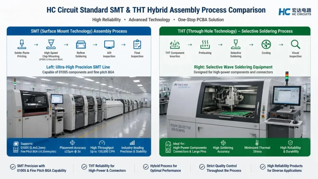
Shenzhen Hongda Circuit SMT & THT Hybrid PCB Assembly Services
Surface-mount technology (SMT) is the dominant assembly method for modern
electronics, handling everything from 01005 passives to fine-pitch BGAs and QFNs. A
typical SMT line runs solder paste printing, high-speed and fine-pitch pick-and-place,
reflow soldering, and automated optical inspection in sequence. Through-hole technology
(THT) remains necessary for connectors, power components, and parts that need the
added mechanical strength of a soldered lead running through the board — these are
placed either by hand or by selective soldering equipment, then wave-soldered or hand
soldered depending on volume.
Most real-world boards mix both technologies, which is why capability sheets for pcb
manufacturing and assembly usually list line counts, placement speed (components per
hour), minimum pitch, and maximum board size side by side. A manufacturer that only
advertises SMT capacity is not equipped for boards with connectors, transformers, or
power modules, so it is worth confirming THT and selective soldering capability explicitly
during supplier qualification.
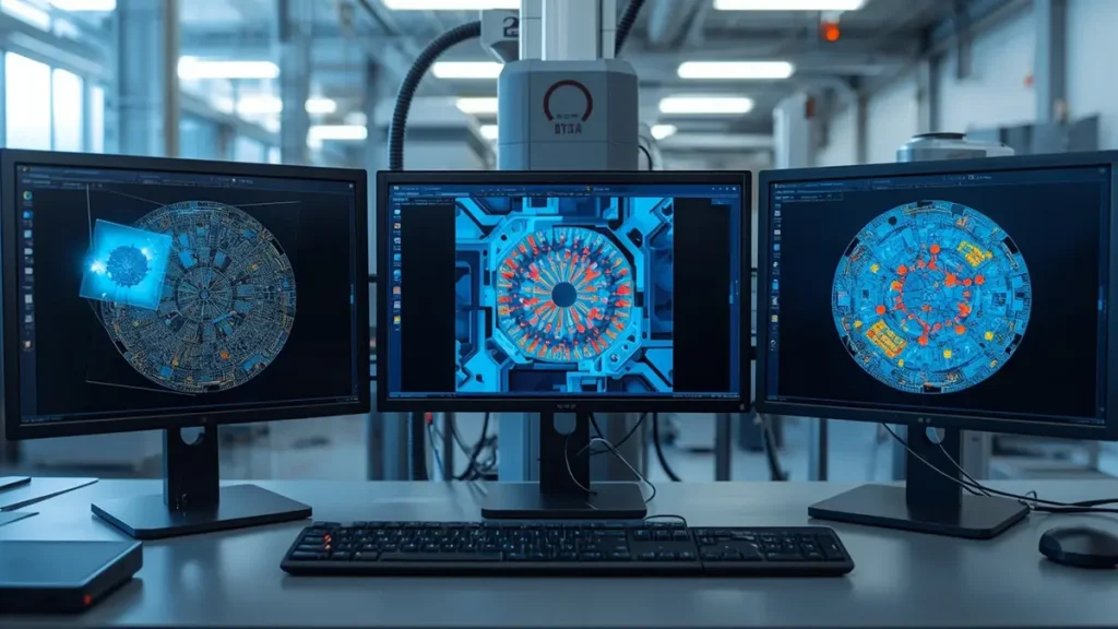
Quality Control: AOI, X-Ray, and Functional Testing in PCB Assembly Services
Shenzhen Hongda Circuit Quality Control System
Quality control is where reputable pcb assembly services separate themselves from low
cost, low-oversight shops. A defensible inspection stack includes:
1. Automated optical inspection (AOI) after paste printing and after reflow, checking
for missing components, solder bridging, tombstoning, and polarity errors.
2. X-ray inspection (AXI) for BGA, QFN, and other packages where the solder joint is
hidden beneath the component body and cannot be verified visually.
3. In-circuit test (ICT) and flying probe test to catch shorts, opens, and incorrect
component values against the schematic.
4. Functional test (FCT) built around the customer’s own test fixture or a jig developed
jointly with the manufacturer, confirming the board actually performs its intended
function, not just that it is electrically continuous.
Traceability matters just as much as the tests themselves. Serialized work orders, reflow
oven temperature profiles logged per batch, and component lot tracking all make it possible
to isolate a root cause quickly if a field failure ever surfaces — a requirement that
automotive and medical customers in particular will ask about directly during an audit.
2026 PCB Manufacturing Technology Trends Shaping PCB Assembly Services
Board designs keep pushing toward higher density, higher speed, and higher power in a
shrinking footprint, and the fabrication and assembly technologies available in 2026 reflect
that pressure. Buyers evaluating a pcb assembly manufacturer today should expect the
following capabilities to be either already in place or on a clearly stated roadmap.
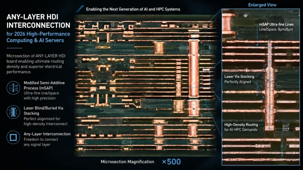
High-Density Interconnect (HDI) and Any-Layer HDI for Next-Gen PCB Fabrication and Assembly
Any-Layer HDI Microsection for AI Server PCB Assembly
HDI boards use microvias, laser drilling, and finer line widths and spacing to pack more
routing into less board area — essential for smartphones, wearables, and compact industrial
controllers. The current frontier is any-layer HDI, built using modified semi-additive
process (mSAP) plating, which allows microvias to stack directly on top of one another
across multiple layers rather than being confined to the outer layers. This matters for pcb
fabrication and assembly because it directly enables smaller form factors without
sacrificing signal integrity, and it is increasingly requested for AI accelerator boards, high
density servers, and 5G/6G radio modules where trace density and impedance control both
need to hold tight tolerances simultaneously.
Advanced Materials for High-Frequency and High-Power PCB Manufacturing and Assembly
Standard FR-4 laminate is not sufficient for every application. High-frequency designs —
RF front ends, radar, satellite communication, and high-speed data links — increasingly
specify low-loss laminates with tightly controlled dielectric constant (Dk) and dissipation
factor (Df) to minimize signal attenuation at gigahertz frequencies. On the power side,
insulated metal substrate (IMS) boards and embedded copper coin technology pull heat
away from power semiconductors far more effectively than standard laminate, which is
why they show up so often in LED lighting, motor drives, and EV charging electronics. A
pcb assembly manufacturer that stocks and reliably processes these materials — rather
than treating them as a special-order exception — is signaling real investment in the
higher-value segment of the market.
AI-Driven Automated Optical Inspection and Smart Factory Integration
Inspection systems have moved well past simple rule-based image comparison. Machine
learning-trained AOI now distinguishes true defects from acceptable process variation with
far fewer false calls, which shortens the review cycle and reduces the chance that a genuine
defect gets waved through by an operator fatigued from chasing false positives all shift.
Paired with manufacturing execution system (MES) software, this generates a closed loop:
inspection data feeds back into placement and reflow parameters in near real time, so a
drifting solder profile gets corrected before it produces a batch of defective boards rather
than after. For buyers, the practical benefit shows up as tighter first-pass yield and more
consistent quality between production runs placed months apart.
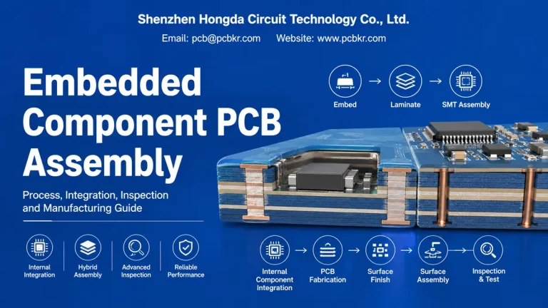
Embedded Component and 3D Packaging Technologies
Space-constrained designs are increasingly embedding passive components — and in
some cases active die — directly inside the PCB substrate rather than mounting them on
the surface. Combined with package-on-package (PoP) and fan-out wafer-level packaging
on the component side, this lets a finished assembly do more in less area, which is
particularly relevant for wearables, hearing aids, and compact IoT sensors. These processes
require assembly partners with correspondingly tighter process control, since a defect
embedded inside a multilayer board is far harder — and more expensive — to rework than
one on the surface.
Lead-Free Soldering, RoHS Compliance, and Supply Chain Resilience in PCB Assembly Services
Environmental compliance is no longer a niche request confined to European-market
products. Lead-free (SAC alloy) reflow profiles are now the default across most pcb
assembly services, and RoHS and REACH compliance documentation is a standard part of
the quote package rather than an add-on that buyers need to specifically ask for. Alongside
compliance, component supply chain resilience has become a recurring topic during
supplier qualification, following several years of allocation cycles on MLCCs,
microcontrollers, and connectors. Manufacturers that maintain approved alternate-part
libraries, multiple distributor relationships, and safety stock on long-lead components are
far better positioned to hold a delivery date than those relying on a single distributor quote
at time of order. Buyers evaluating a pcb assembly manufacturer for a multi-year
production program should ask directly how sourcing risk on long-lead or single-source
components is managed, since that answer often matters more to on-time delivery than the
assembly line’s raw placement speed.
Panel-Level Packaging and Ultra-Fine-Pitch Assembly for AI and High-Performance Computing Boards
The surge in AI accelerator and high-performance computing hardware has pushed
component pitch and panel size in directions that older SMT lines were not built to handle.
Panel-level packaging, larger substrate formats, and ultra-fine-pitch placement below 0.3
mm are becoming routine requirements for server and networking boards rather than a
specialty request. This is one of the clearer dividing lines in the market in 2026: a pcb
assembly manufacturer whose newest placement equipment tops out at standard fine
pitch tolerances simply cannot bid competitively on next-generation compute hardware,
regardless of how strong their general SMT capability is elsewhere in the shop.
How Much Does PCB Assembly Cost? A Transparent Pricing Breakdown
This is, understandably, one of the first questions almost every buyer asks, and it is also one
of the hardest to answer with a single number because so many variables feed into it.
Key Cost Drivers Behind PCB Assembly Services Pricing
1. Board complexity: layer count, board size, and minimum trace/space width all affect
fabrication cost before a single component is placed.
2. Component count and mix: a board with 40 components costs far less to place and
solder than one with 400, and fine-pitch or exotic packages (0201 passives, BGAs,
QFNs) add setup and inspection time.
3. Component sourcing: parts you supply (consignment) versus parts the manufacturer
sources (turnkey) shift both cost and lead-time risk. Turnkey sourcing usually costs a
small premium but protects the schedule against last-minute part shortages.
4. Volume: setup costs — stencils, programming, first-article inspection — are largely
fixed regardless of quantity, so unit cost drops meaningfully as order quantity rises. A
10-unit prototype and a 1,000-unit production run on the identical design can differ in
per-unit cost by several multiples.
5. Testing requirements: adding ICT, functional test fixtures, or burn-in testing
increases cost but reduces the risk of field failures, which is usually the better trade for
safety-critical or high-reliability products.
6. Turnaround time: expedited builds that compress a normal multi-week schedule into
a few days typically carry a rush premium, since they require reprioritizing the line
ahead of other customer orders.
How to Reduce Cost Without Compromising Quality
The most reliable lever is design for manufacturing (DFM) review before the order is placed
rather than after. Standardizing on common component packages, avoiding unnecessarily
tight tolerances where the application does not require them, and consolidating orders to
hit better volume price breaks all reduce cost without touching quality. A capable pcb
assembly manufacturer will flag DFM issues during quoting — inconsistent silkscreen
clearances, components placed too close to board edges, missing fiducials — because
catching them before production avoids costly respins later.
Comparing quotes across suppliers only works if the quotes are structured the same way. A
quote that bundles fabrication, components, and labor into a single line item is far harder to
evaluate than one that itemizes each cost driver separately, because a low total price can
mask an inflated component markup or an unrealistically thin margin on labor that later
shows up as schedule pressure or corner-cutting on inspection. Buyers who request
itemized quotes as a standard part of their RFQ process tend to make better apples-to
apples comparisons and catch pricing anomalies before they sign a purchase order rather
than after production has already started.
How to Order PCB Assembly: A Step-by-Step Guide
How Do PCB Assemblies Get Ordered? From Gerber Files to Finished Boards
The ordering workflow is fairly consistent across reputable suppliers, even if the exact
portal or file format varies:
- Submit design files — Gerber files (or the native CAD output), a bill of materials
(BOM), and a centroid/pick-and-place file that tells the assembly line where each
component sits and in what orientation. - DFM and quote review — the manufacturer checks the files for manufacturability
issues and returns a quote broken down by fabrication, component cost, and assembly
labor. - Component procurement — for turnkey orders, the manufacturer sources parts
against the BOM; for consignment orders, the buyer ships parts directly. - First article / prototype build — especially for a new design, a small pilot batch
confirms fit, function, and process settings before the full order runs. - Production run — the confirmed process moves to full panel quantity, with in-line
AOI and any agreed test steps. - Final inspection, packaging, and shipment — boards are inspected against the
agreed acceptance criteria (commonly IPC-A-610 Class 2 or Class 3), packed to
prevent ESD and mechanical damage, and shipped with the documentation package
the buyer requires.
Buyers researching “how to order pcb assembly” for the first time often underestimate how
much smoother this process runs when the BOM is clean up front — correct manufacturer
part numbers, approved alternates listed for hard-to-source parts, and no ambiguous
reference designators. A few extra minutes spent tightening the BOM before submission
routinely saves days of back-and-forth later.
Choosing Between Prototype PCB Runs and Volume Production
A prototype PCB order should prioritize speed and flexibility — small batch sizes, faster
turnaround, and the ability to make design revisions between iterations without disrupting
a production schedule. Volume production, by contrast, prioritizes cost efficiency and
consistency: locked BOMs, qualified component sources, and process parameters that have
already been validated on the prototype run. Moving from one stage to the other without
re-validating the design on production tooling is a common and avoidable source of yield
problems, so it is worth confirming with your supplier whether the prototype and
production builds will use the same stencils, fixtures, and process settings.
How to Choose a Reliable PCB Assembly Manufacturer
Certifications and Capability Checklist for PCB Fabrication and Assembly Partners
A short list of things worth verifying directly rather than taking on faith from a website:
1. ISO 9001 as a baseline quality management certification, with IATF 16949 for
automotive programs and ISO 13485 for medical device work.
2. IPC-A-610 and J-STD-001 certified operators, and clarity on which acceptance class
(Class 2 for general industrial electronics, Class 3 for high-reliability applications) the
line is qualified against.
3. UL certification for the facility where relevant to the end product.
4. Documented traceability from component lot to finished serial number.
5. Line capacity and equipment list — placement speed, minimum component pitch,
maximum board dimensions, and whether both SMT and THT assembly are handled
in-house.
6. Communication and engineering support — how quickly DFM feedback comes
back, and whether an actual engineer reviews the files rather than a sales contact
simply forwarding the quote request.
None of these items are hard to ask about, but they are surprisingly easy to skip during a
fast quoting cycle when a buyer is juggling several supplier conversations at once. A short
standard checklist, applied consistently to every new supplier under evaluation, catches
gaps that a single rushed phone call usually misses — and it gives procurement a
documented basis for the selection decision if it is ever questioned internally or during a
customer audit further down the supply chain.
Why Shenzhen Hongda Circuit Technology Co., Ltd. Is Built for 2026 Manufacturing Demands
Shenzhen Hongda Circuit Technology Co., Ltd. runs PCB fabrication and assembly under
one roof, which keeps engineering changes, DFM feedback, and schedule commitments in
a single line of communication rather than split across separate vendors. The production
floor supports mixed SMT and THT lines for standard FR-4 designs alongside HDI, high
frequency laminate, and metal-core builds for power and RF applications, backed by AOI, X
ray, and functional test stations at each stage of the process. For buyers moving from a
custom PCB prototype into full production, that means the same process parameters and
quality documentation carry through both stages instead of resetting at a hand-off between
suppliers. The engineering team reviews Gerber, BOM, and centroid files directly during
quoting, which is where most avoidable delays get caught before they ever reach the
production floor.
Industries and Applications Served by Modern PCB Fabrication and Assembly
Different end markets place very different demands on a pcb assembly manufacturer, and
understanding where a supplier’s real strength lies — rather than assuming a general
purpose line can handle everything equally well — saves buyers from a mismatch
discovered only after a failed audit or a field return.
Industrial, Automotive, and Power Electronics PCB Manufacturing and Assembly
Industrial control boards, motor drives, and automotive electronics share a common
demand for durability across wide temperature ranges, vibration, and long service life,
often ten years or more in the field. This is where metal-core boards, embedded copper coin
thermal management, and IATF 16949-aligned process control matter most, since a power
supply or motor controller failing in the field carries a much higher cost than a consumer
gadget field return. Buyers in this segment typically prioritize documented process stability
and long-term component availability over the fastest possible turnaround time.
Communications, Networking, and AI Infrastructure PCB Assembly Services
5G radio units, networking switches, and AI server boards sit at the opposite end of the
spectrum: extremely tight signal integrity requirements, high layer counts, and
increasingly, any-layer HDI construction with low-loss laminate. These programs tend to
move fast, with design revisions arriving between prototype rounds, so an assembly
partner’s engineering responsiveness and ability to turn around a revised stencil or fixture
quickly can matter as much as raw production capacity.
Consumer Electronics and IoT: Balancing Cost, Density, and Speed to Market
Consumer and IoT products compete primarily on cost and time to market, which puts
pressure on component sourcing efficiency and DFM discipline early in the design cycle —
a board redesigned twice because of an avoidable placement issue can cost a product its
launch window. High component density in a small form factor, frequently paired with
embedded passives or fan-out packaging, is now common even in mid-range consumer
devices, not just flagship products.
PCB Assembly Services FAQ: Answers Procurement Teams Search For
What is the difference between PCB fabrication and PCB assembly?
PCB fabrication produces the bare board itself — the copper traces, layers, and solder mask etched onto a substrate. PCB assembly is the subsequent step of placing and soldering components onto that bare board to create a functioning printed circuit board assembly (PCBA). Buyers requesting “pcb manufacturing and assembly” from a single vendor are asking for both
steps combined under one purchase order.
How much does PCB assembly typically cost for a small prototype run?
Cost depends heavily on component count, board complexity, and whether parts are supplied by the buyer or sourced by the manufacturer, so there is no single figure that applies across designs. What buyers can control is the request for an itemized quote that separates fabrication, component, and assembly labor costs, which makes it possible to compare suppliers on equal terms and identify exactly where cost is concentrated.
How do I know if a PCB assembly manufacturer can handle my specific board design?
Send the actual Gerber files, BOM, and centroid file for a DFM review rather than relying on a general capability sheet. A manufacturer’s response to that review — whether they flag real manufacturability issues, ask specific questions about tolerances, and quote a realistic
lead time — is a far more reliable signal of fit than the capability list on their homepage.
What lead time should I expect between placing an order and receiving finished PCB assemblies?
Lead time varies with board complexity, component availability, and order
volume, and it typically differs meaningfully between a prototype build and a full production run. The most useful step a buyer can take is requesting a lead-time commitment broken out by fabrication, component procurement, and assembly, since component sourcing is usually the variable most likely to shift the overall schedule.
What documentation should a PCB assembly supplier provide with a finished order?
At minimum, expect a certificate of conformance, test reports for any agreed inspection or functional testing, and traceability records linking component lots to the finished assembly. For regulated industries — automotive, medical, aerospace — confirm in advance which specific certifications (IATF 16949, ISO 13485, AS9100) and inspection classes (IPC-A-610 Class 2 or Class 3) the documentation package will reference, since requirements differ by end application.
About Author
David Chen https://www.linkedin.com/in/pcbcoming
David Chen boasts an extensive professional background in PCBA manufacturing, PCBA testing, and PCBA optimization, with specialized expertise in high-precision PCBA fault analysis and rigorous PCBA reliability testing. The author has worked with high-layer-count server PCB fabrication, ultra-low-loss backplane stackups, and thermo-mechanical reliability optimization for AI infrastructure projects involving 112G and 224G PAM4 architectures. Skilled in complex circuit design and cutting-edge advanced PCB manufacturing processes, he delivers solutions that elevate product durability and performance across industrial applications. His technical articles focusing on PCBA manufacturing workflows and testing methodologies are widely cited by industry peers, research institutions, and technical platforms, solidifying his reputation as a recognized technical authority in the global circuit board manufacturing sector.