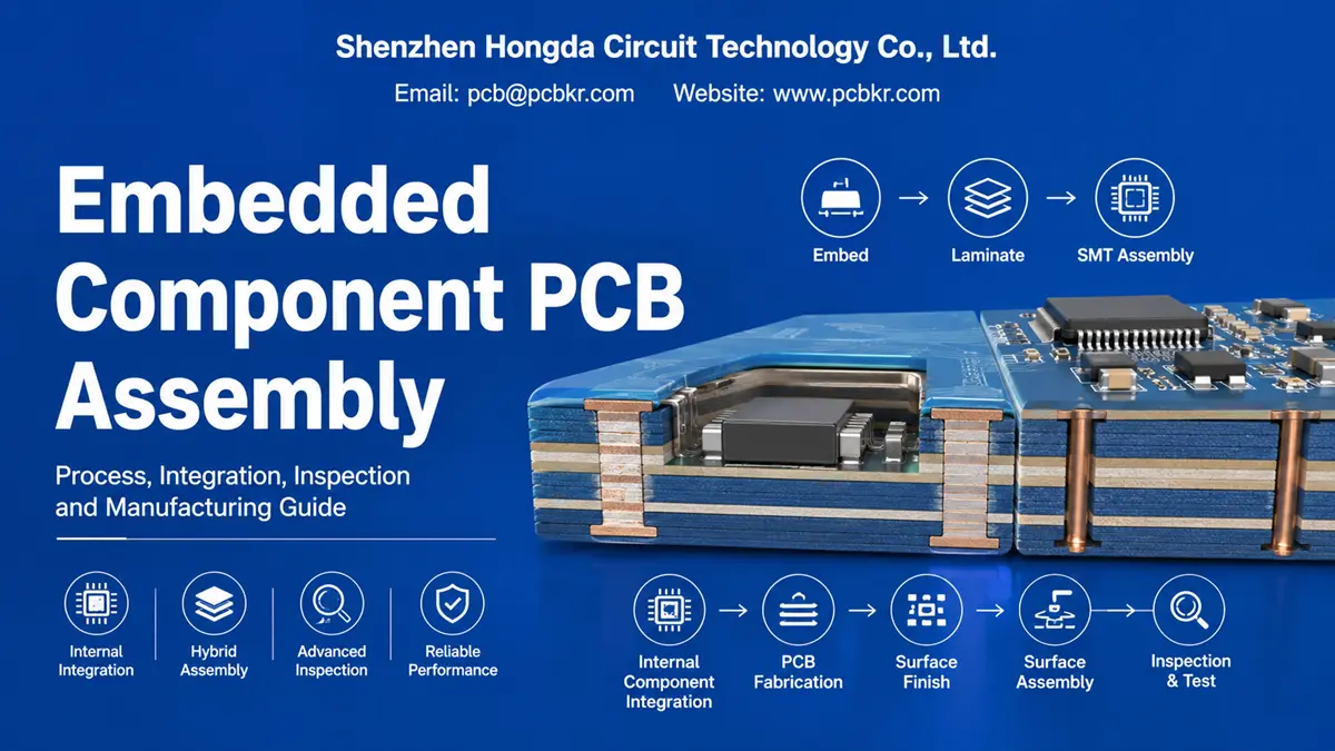
Embedded Component PCB Assembly: Engineering and Manufacturing Guide
Embedded component PCB assembly differs from conventional SMT assembly because some components are integrated into the PCB before conventional surface assembly begins. The manufacturing challenge is coordinating internal component integration with the subsequent outer-layer SMT process.
What Is Embedded Component PCB Assembly?
Embedded component PCB assembly is the process of integrating selected electronic components into internal PCB structures and subsequently completing any required external component assembly.
A typical product may therefore contain both:
- Internally embedded components
- Externally mounted SMT components
- Through-hole components where required
The internal and external assembly operations must be treated as a connected manufacturing sequence. For end‑to‑end technology overview, design challenges and supplier procurement evaluation criteria, please refer to our Embedded Component PCB: Technology, Manufacturing & Procurement Guide.
How Does Embedded Assembly Differ From Conventional SMT?
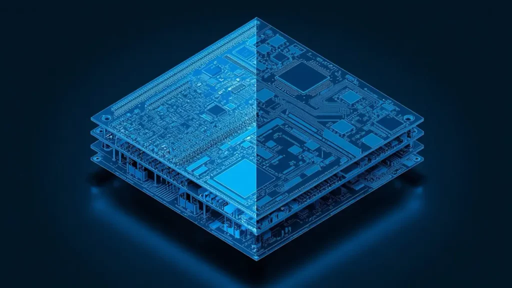
3D Cross-Section Comparison of Embedded PCB vs Conventional SMT Assembly
In conventional SMT, the component is placed directly onto an accessible PCB surface.
In embedded assembly, the component may be positioned inside a cavity or internal structure before the PCB is fully laminated.
| Feature | Embedded Component Assembly | Conventional SMT |
|---|---|---|
| Component location | Internal and/or surface | Mainly surface |
| Accessibility | Some components inaccessible after lamination | Accessible |
| Placement sequence | Integrated into PCB fabrication | After PCB fabrication |
| Rework | Difficult after embedding | Relatively accessible |
| Inspection | Requires internal inspection methods | Primarily surface inspection |
| Process coupling | High | Lower |
The important distinction is that embedding turns component placement into part of PCB fabrication.
What Components Can Be Used in Embedded Assembly?
Common categories include:
- Resistors
- Capacitors
- Inductors
- Passive networks
- Selected active devices
- Semiconductor dies
The manufacturing requirements vary considerably between passive and active devices.
Passive embedding is generally easier to integrate because thermal and mechanical requirements may be less demanding than those associated with active semiconductor devices.
How Are Embedded Components Positioned?
Component placement normally requires controlled X/Y positioning and orientation.
The placement process should consider:
- Cavity dimensions
- Component body tolerance
- Pad geometry
- Electrical connection points
- Lamination clearance
- Adjacent copper structures
- Thermal requirements
For fine-pitch embedded structures, vision-assisted alignment can provide a higher degree of process control than manual placement.
How Are Embedded Components Electrically Connected?
The connection architecture depends on the component and PCB construction.
Possible approaches include:
- Direct pad connections
- Microvias
- Via-in-pad
- Copper-filled vias
- Fine-line redistribution structures
The interconnection strategy must be established before production because the embedded component’s position determines the location of downstream PCB structures.
Why Is Lamination Part of Embedded Component Assembly?
In conventional SMT, solder reflow is normally a major assembly operation.
For embedded components, however, lamination can become part of the component integration process.
The embedded device must survive:
- Thermal exposure
- Mechanical pressure
- Resin flow
- Vacuum conditions
- Chemical processing
- Subsequent drilling and plating
Therefore, the component itself becomes a manufacturing-process constraint.
How Is SMT Completed After Embedding?
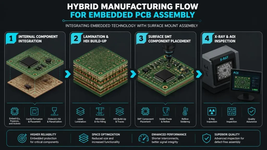
Step-by-Step Hybrid Manufacturing Flow for Embedded PCB Assembly
A hybrid manufacturing flow may look like:
Internal Component Integration → Lamination → HDI Build-Up → PCB Fabrication → Surface Finish → SMT Placement → Reflow → Inspection → Electrical Test
This approach allows a single product to combine internal integration with conventional external assembly.
What Are the Main Inspection Challenges?
Once an embedded component is laminated inside the board, visual access is lost.
Inspection can therefore require:
- X-ray inspection
- 3D inspection
- Electrical testing
- Cross-section analysis
- Process traceability
For external SMT components, AOI can inspect solder joints and component placement.
For internal structures, X-ray and destructive analysis can provide additional visibility.
How Should Embedded Assembly Be Qualified?
Prototype builds should verify:
- Component placement
- Cavity compatibility
- Lamination integrity
- Electrical connectivity
- Microvia integrity
- External SMT compatibility
- Thermal behavior
- Production repeatability
A successful prototype does not automatically establish mass-production capability.
The manufacturing process should therefore include a transition plan from prototype to volume production.
Key Takeaway
Embedded component PCB assembly is best understood as PCB fabrication plus internal component integration plus conventional assembly where required.
The most important engineering consideration is process coordination. Component placement, cavity design, lamination, interconnection and final SMT assembly must work together rather than being optimized independently.
What is the main difference between Embedded Component Assembly and Conventional SMT Assembly?
The fundamental distinction between Embedded Component Assembly and Conventional SMT Assembly lies in component placement location and manufacturing process coupling.
1. Component Location: Conventional SMT places components on external, accessible PCB surfaces, whereas embedded assembly integrates selected components into internal PCB structures or cavities (often combined with external surface placement).
2. Manufacturing Sequence: Conventional SMT occurs strictly after PCB fabrication is complete, while embedded placement becomes an integral part of the PCB fabrication and lamination process itself.
3. Inspection & Rework: SMT solder joints remain visible and accessible for AOI inspection and rework, whereas embedded components lose visual accessibility once laminated, requiring specialized non-destructive internal inspection methods (e.g., X-ray) and making rework extremely difficult.
How does embedding passive devices compare to active semiconductor devices?
In embedded PCB manufacturing, integrating passive devices (resistors, capacitors, inductors) differs significantly from active devices (semiconductor dies, ICs) in terms of process complexity and material constraints:
Passive Device Embedding:
Process Complexity: Generally easier to integrate.
Thermal & Mechanical Demands: Less demanding, as passives tolerate the mechanical pressure and thermal cycles of lamination better.
Active Semiconductor Embedding:
Process Complexity: Considerably higher.
Thermal & Mechanical Demands: Extremely stringent; active dies require precise alignment (often vision-assisted) and fine-pitch interconnection structures (such as microvias or redistribution layers) to withstand lamination forces and maintain reliability.
How do electrical connection methods differ between embedded components and conventional SMT pads?
Conventional SMT relies on surface solder paste and reflow soldering to form electrical and mechanical joints. In contrast, embedded components are interconnected within internal layers during HDI build-up and lamination.
Key electrical connection architectures for embedded components include:
Microvias & Copper-Filled Vias: Laser-drilled and electroplated to build direct electrical paths to internal component pads.
Via-in-Pad: Optimizes density and shortens signal paths.
Fine-Line Redistribution Structures: Used for high-density active semiconductor die fan-out.
Direct Pad Connections: Configured within internal copper layers prior to lamination.
What are the main inspection challenges of embedded PCB assembly compared to surface assembly?
Visual access is completely lost once embedded components are enclosed during lamination, shifting the inspection paradigm from surface optics to internal volume imaging:
Conventional SMT Inspection: Relies primarily on Automated Optical Inspection (AOI) and visual checks to evaluate solder joints, alignment, and bridging.
Embedded Assembly Inspection:
X-Ray Inspection: Evaluates internal alignment, voiding, and microvia connectivity non-destructively.
3D Internal Inspection: Assesses structural integrity inside multi-layer builds.
Destructive Cross-Section Analysis: Used during prototype qualification to verify lamination integrity and interface plating.
Process Traceability & Electrical Test: Tracks manufacturing parameters and functional integrity across internal layers.
How does lamination in embedded assembly compare to reflow soldering in conventional SMT?
While solder reflow is the primary thermal joining step in conventional SMT, lamination serves as a key component-integration step in embedded assembly:
Conventional Reflow: Components are subjected mainly to controlled thermal profiles under ambient pressure without severe physical mechanical loads.
Embedded Lamination: Embedded components must survive a much harsher, combined stress environment involving high mechanical pressure, thermal exposure, resin flow, vacuum conditions, and subsequent drilling/plating chemicals. Consequently, the embedded component itself becomes a critical constraint on the entire PCB manufacturing process.
About Author
David Chen https://www.linkedin.com/in/pcbcoming
David Chen boasts an extensive professional background in PCBA manufacturing, PCBA testing, and PCBA optimization, with specialized expertise in high-precision PCBA fault analysis and rigorous PCBA reliability testing. The author has worked with high-layer-count server PCB fabrication, ultra-low-loss backplane stackups, and thermo-mechanical reliability optimization for AI infrastructure projects involving 112G and 224G PAM4 architectures. Skilled in complex circuit design and cutting-edge advanced PCB manufacturing processes, he delivers solutions that elevate product durability and performance across industrial applications. His technical articles focusing on PCBA manufacturing workflows and testing methodologies are widely cited by industry peers, research institutions, and technical platforms, solidifying his reputation as a recognized technical authority in the global circuit board manufacturing sector.