Embedded Component PCB Manufacturing Process: Step-by-Step Guide
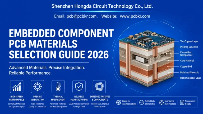
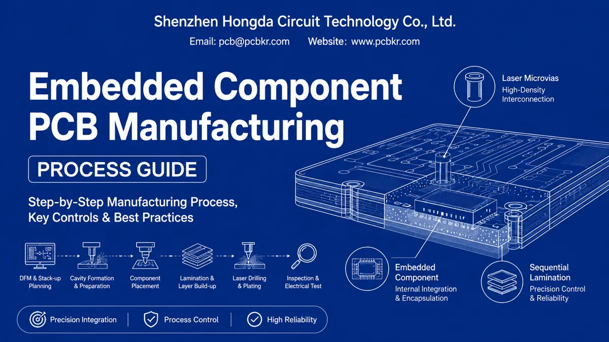
An embedded component PCB requires a controlled manufacturing sequence that integrates component placement with PCB fabrication. The critical process stages include inner-layer preparation, cavity formation, component placement, lamination, laser drilling, plating, routing, surface finishing, inspection and electrical verification.
Unlike a conventional multilayer PCB, embedded-component fabrication cannot treat PCB fabrication and component integration as independent operations. The position and physical characteristics of the embedded device must remain compatible with subsequent lamination, drilling, interconnection and inspection processes.
What Is the Embedded Component PCB Manufacturing Process?
The embedded component PCB manufacturing process is a coordinated sequence in which selected components are incorporated into internal PCB structures during board fabrication.
A typical process can be organized as:
DFM → Material Preparation → Inner-Layer Circuit Formation → Cavity Formation → Component Placement → Lamination → Laser Drilling → Plating/Copper Filling → Outer-Layer Processing → Surface Finish → Inspection → Electrical Test
The exact sequence depends on the component type, PCB construction, cavity architecture and interconnection technology. For broader design, procurement and supplier‑evaluation guidance covering embedded active and passive devices, refer to our Embedded Component PCB: Technology, Manufacturing & Procurement Guide.
How Is the PCB Stack-Up Prepared for Embedded Components?
The process begins with a manufacturing stack-up designed around the embedded component rather than simply adding the component to an existing conventional stack-up.
Engineers must coordinate:
- Core and prepreg structures
- Copper thickness
- Component thickness
- Cavity depth
- Dielectric thickness
- Microvia locations
- Thermal expansion
- Lamination requirements
- Final board thickness
The component’s Z-height is particularly important. A component that physically fits into a cavity may still create excessive local pressure or dielectric-flow problems during lamination.
Therefore, cavity depth, component thickness and surrounding dielectric construction must be considered together.
How Are Embedded Component Cavities Manufactured?
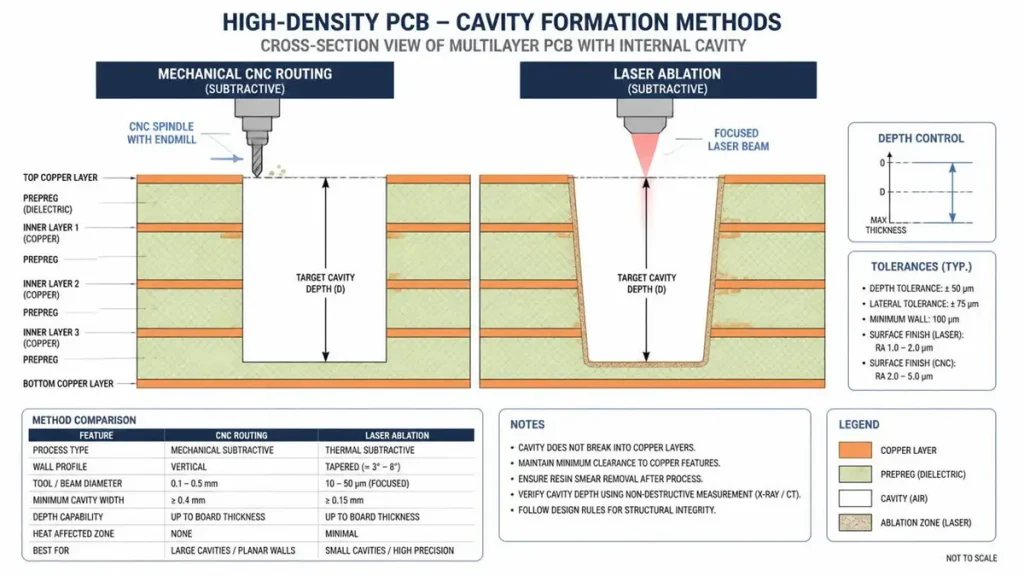
Comparison of Mechanical CNC Routing vs. Laser Ablation for PCB Cavity Formation in Embedded Component Manufacturing
Cavity formation is one of the defining manufacturing steps.
Depending on the PCB architecture, cavities may be created using:
- Mechanical routing
- CNC machining
- Laser processing
- Specialized depth-controlled processes
The objective is not simply to create an opening.
The cavity must provide:
- Sufficient component clearance
- Controlled depth
- Correct X/Y positioning
- Adequate mechanical support
- Compatible dielectric and adhesive conditions
- Stable dimensions through subsequent processing
For high-density embedded PCBs, cavity registration becomes increasingly important because subsequent microvias and fine-line structures may reference the embedded component position.
How Are Components Placed Inside the PCB?
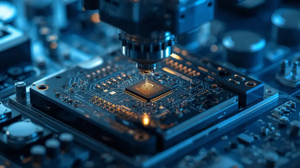
Precision Placement of Microscopic Components into Embedded PCB Cavities
After cavity preparation, the embedded component is positioned according to the PCB reference system.
Component placement must account for:
- Component orientation
- X/Y location
- Component height
- Pad position
- Cavity clearance
- Adhesive or dielectric interaction
- Subsequent lamination pressure
Vision-assisted placement can help improve positioning consistency.
The key manufacturing principle is that component placement accuracy cannot be evaluated independently from downstream via and routing registration.
Why Is Lamination Critical for Embedded Component PCBs?
Lamination is one of the most sensitive stages because pressure and temperature affect both the PCB structure and the embedded component.
During lamination, manufacturers must control:
- Temperature profile
- Pressure
- Resin flow
- Vacuum conditions
- Dielectric thickness
- Component protection
- Board registration
- Warpage
An embedded component changes the local mechanical structure of the PCB.
Consequently, a lamination process that works for a conventional multilayer board may require modification for an embedded structure.
Poor process control can result in:
- Voids
- Delamination
- Component displacement
- Resin-flow problems
- Internal stress
- Dimensional instability
How Are Microvias Connected to Embedded Components?
After the embedded structure has been laminated, laser drilling may be used to create microvias connecting build-up layers.
Typical structures include:
- Staggered microvias
- Stacked microvias
- Via-in-pad structures
- Copper-filled microvias
Laser drilling provides a practical way to establish fine electrical connections without consuming as much routing space as conventional through-hole structures.
The exact drilling method depends on the dielectric system, copper structure, via diameter and required aspect ratio.
Why Is Copper Filling Important?
Copper filling can provide both electrical and structural functions.
For example, copper-filled microvias can support:
- Layer-to-layer interconnection
- Via-in-pad structures
- High-density routing
- Improved connection reliability
The quality of the filled via depends on process control during:
Laser drilling → Desmear → Activation → Plating → Copper filling → Surface preparation
Incomplete filling or defects around the microvia can become reliability risks later in the product lifecycle.
How Are Embedded Component PCBs Inspected During Manufacturing?
A major manufacturing challenge is that important structures are hidden inside the PCB.
Consequently, inspection cannot depend only on conventional surface inspection.
Manufacturers may combine:
- AOI
- 3D inspection
- X-ray inspection
- Cross-section analysis
- Dimensional inspection
- Electrical testing
- Process traceability
The inspection strategy should be developed around the actual failure mechanisms of the embedded construction.
For example, a surface AOI system cannot directly confirm every internal component-positioning or lamination condition.
What Are the Most Critical Manufacturing Controls?
For embedded component PCB production, the highest-value controls normally occur around:
| Manufacturing Stage | Critical Control |
|---|---|
| Stack-up | Component-to-layer relationship |
| Cavity | Depth and dimensional accuracy |
| Placement | X/Y position and orientation |
| Lamination | Pressure, temperature and void control |
| Laser drilling | Via diameter and registration |
| Plating | Interconnection integrity |
| Routing | Mechanical dimensional control |
| Inspection | Hidden-structure visibility |
| Electrical test | Open/short and connectivity |
| Process records | Lot-level traceability |
This is why embedded PCB manufacturing should be managed as an integrated process rather than a sequence of isolated operations.
What Manufacturing Data Should a Supplier Provide?
For technically demanding projects, procurement teams should request evidence such as:
- Manufacturing capability documentation
- Cross-section samples
- Cavity inspection data
- Microvia inspection results
- X-ray records where applicable
- Electrical test results
- Yield information
- Process-control records
- Prototype-to-production validation information
The purpose is to establish whether the supplier can repeat the process, not merely manufacture one successful prototype.
Key Takeaway
The defining feature of embedded component PCB manufacturing is process integration. Cavity formation, component placement, lamination, laser drilling, plating and inspection must be controlled as one manufacturing system.
The objective is therefore not simply to manufacture an embedded PCB once, but to establish a repeatable process capable of maintaining dimensional accuracy, interconnection integrity and production yield.
What is the primary difference between Embedded Component PCB and Conventional PCB manufacturing?
The essential difference is process integration. Conventional PCB manufacturing treats bare board fabrication and surface component assembly as two independent, sequential operations. Embedded component PCB fabrication integrates component placement directly into the internal layer sequence before final board lamination, making component assembly and board fabrication an inseparable single system.
1. Process Logic: Conventional PCB follows a sequential path (Bare board fabrication $\rightarrow$ Surface SMT assembly). Embedded PCB uses an integrated path where component placement occurs during inner-layer core build-up.
2. Component Location: Conventional components sit externally on top or bottom surface pads. Embedded components reside internally, encapsulated within core, prepreg, or cavity dielectrics.
3. Interconnection Method: Conventional boards use surface solder paste reflow. Embedded boards rely on direct laser microvias and electroplated copper filling connected directly to component pads.
4. Inspection Approach: Conventional boards use 2D optical AOI, visual inspection, and ICT. Embedded boards require penetrative 3D X-ray (CT), acoustic microscopy (SAM), and micro-sectioning.
5.Reworkability: Conventional surface components can be desoldered and repaired. Embedded defects are completely unrecoverable and result in immediate board scrap.
How does Mechanical Routing compare to Laser Machining for PCB cavity formation?
Mechanical CNC routing relies on physical cutting tools best suited for large, deep cavities requiring high material removal rates. Laser machining uses pulsed light energy to ablate material, offering the precise depth control and micro-scale geometry needed for High-Density Interconnect (HDI) structures and ultra-thin bare die encapsulation.
1. Depth Accuracy: Mechanical routing is limited by physical tool wear (within +/- 25 microns). Laser machining provides high-precision pulse ablation control (within +/- 10 microns).
2. Target Components: Mechanical routing targets standard discrete passives, modules, and thick active ICs. Laser machining handles thin bare dies and ultra-small 0201 or 01005 passives.
3. Edge Quality: Mechanical routing introduces physical stress with potential micro-burrs or delamination. Laser machining offers non-contact, clean edges but requires Heat-Affected Zone (HAZ) management.
4. Cost Efficiency: Mechanical routing is highly cost-effective for large cavity volumes. Laser machining carries higher tool and equipment costs, making it optimal for micro-cavities.
How does Lamination for Embedded PCBs differ from Standard Multilayer Lamination?
Standard lamination manages resin flow to encapsulate planar copper circuits. Embedded PCB lamination must achieve void-free resin encapsulation around complex 3D internal components without crushing the device, causing lateral displacement, or inducing extreme thermal stress in the dielectric matrix.
1. Thermal & Pressure Profile: Standard lamination uses single-stage pressure and temperature ramps. Embedded lamination requires multi-stage stepped pressure cycles and gradual thermal ramps.
2. Resin Hydrodynamics: Standard lamination fills planar copper trace gaps. Embedded lamination requires precise, controlled resin displacement to fill cavity clearances without creating voids.
3.Mechanical Stress: Standard lamination maintains uniform stress distribution across layers. Embedded lamination produces high localized stress concentration along rigid component edges.
4.Registration Control: Standard lamination manages layer-to-layer copper artwork alignment. Embedded lamination must strictly control X/Y component drift caused by lateral resin shear flow.
Why are Laser Microvias preferred over Mechanical Drills for embedded interconnections?
Mechanical drilling creates through-holes that penetrate the entire board stackup, taking up valuable routing area across all layers. Laser microvias allow direct, high-density vertical z-axis connections from build-up layers straight to embedded component pads (Via-in-Pad) without wasting inner-layer real estate.
1. Via Diameter: Mechanical drilling produces holes typically greater than or equal to 150 microns. Laser microvias achieve diameters from 50 microns to 100 microns.
2. Routing Impact: Mechanical drills penetrate all layers and block routing channels throughout the stackup. Laser microvias are blind or buried, terminating directly on the embedded pad.
3. Physical Stress: Mechanical drilling exerts high vibration and physical drill pressure. Laser microvias use non-contact beam delivery with zero mechanical impact on delicate components.
4. Plating Standard: Mechanical through-holes use standard thin-wall electrolytic copper plating. Laser microvias require electroplated copper filling to enable stacked via structures.
How does Inspection for Embedded Component PCBs differ from Standard Optical AOI?
Standard PCB inspection relies on surface-level 2D Automated Optical Inspection (AOI) to verify exposed conductors. Because embedded components and microvias are entirely encapsulated within internal dielectric layers, embedded PCB inspection relies on penetrative non-destructive testing (AXI/3D CT) and destructive physical cross-sectioning.
1. Primary Inspection Tool: Standard inspection uses surface 2D Optical AOI and automated solder inspection. Embedded inspection uses Automated X-ray Inspection (AXI) and 3D X-ray CT scans.
2. Defect Target: Standard inspection detects surface shorts, opens, solder bridging, and surface contamination. Embedded inspection targets internal resin voids, component tilt or shift, and internal micro-cracks.
3. Interconnection Audit: Standard inspection uses visual checks and basic electrical continuity. Embedded inspection requires metallographic cross-sectioning and thermal shock stress analysis.
4. Traceability Scope: Standard inspection tracks bare-board lot numbers. Embedded inspection implements dual-level tracking for both the PCB lot and individual embedded component serial numbers.
About Author
David Chen https://www.linkedin.com/in/pcbcoming
David Chen boasts an extensive professional background in PCBA manufacturing, PCBA testing, and PCBA optimization, with specialized expertise in high-precision PCBA fault analysis and rigorous PCBA reliability testing. The author has worked with high-layer-count server PCB fabrication, ultra-low-loss backplane stackups, and thermo-mechanical reliability optimization for AI infrastructure projects involving 112G and 224G PAM4 architectures. Skilled in complex circuit design and cutting-edge advanced PCB manufacturing processes, he delivers solutions that elevate product durability and performance across industrial applications. His technical articles focusing on PCBA manufacturing workflows and testing methodologies are widely cited by industry peers, research institutions, and technical platforms, solidifying his reputation as a recognized technical authority in the global circuit board manufacturing sector.