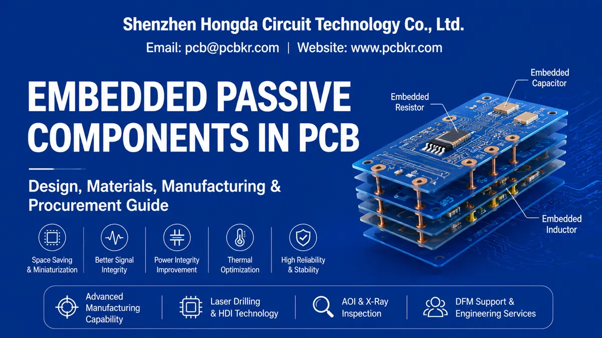
Embedded Passive Components in PCB: Design, Materials, Manufacturing & Procurement Guide
What Are Embedded Passive Components in a PCB?
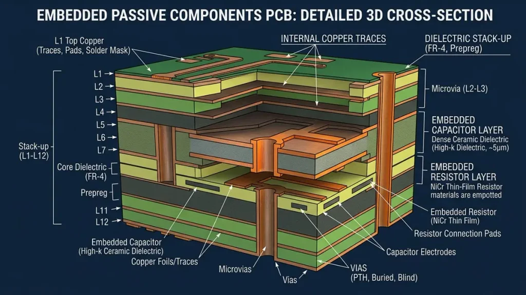
3D Cross-Section Diagram of Embedded Passive Components PCB Architecture
Direct answer: Embedded passive components are resistive, capacitive, or inductive functions integrated into the internal structure of a printed circuit board instead of being placed exclusively as conventional surface-mounted parts. This approach allows designers to use internal PCB volume for electrical functions while preserving valuable outer-layer space.
The concept is broader than simply placing a discrete resistor or capacitor inside a cavity.
An Embedded Passive PCB can implement passive functions through several approaches, including:
- Discrete embedded resistors
- Discrete embedded capacitors
- Embedded inductors
- Resistive films or resistive materials
- Capacitive dielectric structures
- Integrated passive networks
- Passive structures formed directly within PCB layers
This distinction matters because the electrical behavior of an embedded passive component depends not only on the component itself, but also on the surrounding copper, dielectric material, layer geometry, vias and return paths.
For engineering teams, an Embedded Passive Components PCB should therefore be treated as an integrated electrical and manufacturing structure rather than simply a conventional PCB with components moved underneath the surface. See our Embedded Component PCB: Technology, Manufacturing & Procurement Guide for the full scope including embedded active devices and die embedding.
Why Are Embedded Passive Components Becoming More Important?
PCB design is increasingly constrained by the amount of functional circuitry that must fit into a fixed mechanical envelope.
At the same time, electronic systems are placing greater demands on:
- Component density
- Power integrity
- Signal integrity
- Electrical path length
- Thermal management
- Electromagnetic behavior
- Mechanical thickness
- Assembly space
A conventional PCB normally uses the outer surfaces for most discrete passive components. As the number of components increases, these surfaces become crowded.
Embedding selected passive functions creates another design dimension: the internal PCB structure itself becomes part of the component architecture.
This can be particularly useful when a product requires a smaller form factor without simply reducing component functionality.
The engineering objective is therefore not:
“Embed as many components as possible.”
A better objective is:
“Embed the passive functions that provide the greatest system-level benefit for the additional manufacturing complexity.”
That distinction should guide both design and procurement decisions.
What Types of Passive Components Can Be Embedded in a PCB?
Embedded Resistors
Embedded resistors can be implemented using discrete resistor components or specially formulated resistive materials integrated into PCB layers.
Depending on the design approach, resistive structures can be used for:
- Bias networks
- Pull-up and pull-down functions
- Termination
- Current limiting
- Voltage division
- Signal conditioning
One advantage of a resistive layer structure is that the resistor function does not necessarily require a conventional component package occupying surface area.
However, resistance tolerance, temperature coefficient, material uniformity and process variation must be considered during design.
Embedded Capacitors
Embedded capacitors are particularly interesting for power distribution and high-speed electronic systems.
A capacitor is created through conductive layers separated by a dielectric.
When this structure is incorporated into the PCB stack-up, the electrical distance between the capacitor and the circuit can be significantly reduced compared with some conventional surface-mounted arrangements.
Applications may include:
- Local decoupling
- Power distribution
- High-frequency bypassing
- Noise control
- Power integrity optimization
The effectiveness of an embedded capacitor depends strongly on dielectric properties, electrode geometry and interconnection inductance.
Embedded Inductors
Embedded inductors can be created through PCB trace geometry, magnetic materials or specialized multilayer structures.
They may be considered for:
- Filtering
- RF circuits
- Power conversion
- Matching networks
- Electromagnetic functions
Compared with embedded resistors and capacitors, inductors generally require more careful electromagnetic modeling because their performance depends strongly on geometry and surrounding structures.
How Does an Embedded Resistor PCB Work?
There are two broad engineering approaches to embedded resistance.
The first uses a discrete resistor element integrated into the PCB.
The second uses a resistive material or resistive film to form the required resistance directly within the PCB structure.
The second approach can be attractive when many small resistance functions are required.
Instead of:
PCB → solder pad → resistor package → solder joint
the electrical function may become:
PCB copper → resistive layer → PCB interconnection
This can eliminate selected surface-mounted packages and solder joints.
However, the design engineer must understand that the resistance value is determined by the resistive material and its geometry.
Important parameters include:
- Sheet resistance
- Resistor dimensions
- Pattern geometry
- Material tolerance
- Temperature coefficient
- Processing variation
- Contact geometry
- Operating temperature
A supplier should therefore provide appropriate material and process data before the design is released for production.
How Does an Embedded Capacitor PCB Work?
An Embedded Capacitor PCB uses conductive layers and dielectric material to create capacitance within the PCB stack-up.
The basic electrical principle can be represented conceptually as:
Copper electrode → dielectric → copper electrode
The capacitance is influenced by:
- Electrode area
- Dielectric thickness
- Dielectric constant
- Material uniformity
- Operating temperature
- Frequency
The major engineering attraction is the physical proximity between the capacitance and the circuit that needs it.
For high-speed power delivery, reducing the physical distance between power and ground structures can reduce the impact of interconnection inductance.
This is why embedded capacitance can be considered as part of a broader power integrity strategy, rather than simply a component-count reduction technique.
What Is the Difference Between Embedded Passive Components and Surface-Mounted Passives?
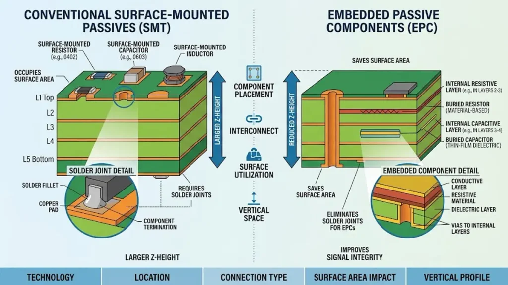
Comparison Diagram: Conventional SMT vs. Embedded Passive Components PCB
| Design consideration | Embedded Passive Components | Conventional Surface-Mounted Passives |
|---|---|---|
| Component location | Internal PCB structure | PCB surface |
| Surface area | Lower usage | Higher usage |
| Solder joints | Can be reduced | Required for discrete parts |
| Electrical path | Potentially shorter | Often longer |
| Inspection | More difficult | Easier |
| Repairability | Limited | Relatively easy |
| Design freedom | High | High |
| Manufacturing complexity | Higher | Lower |
| Thermal interaction | Closely tied to PCB structure | More accessible |
| Component replacement | Difficult | Relatively straightforward |
| Best use case | Space-constrained/high-density designs | General electronics |
The comparison should not be interpreted as meaning embedded passives are always superior.
A surface-mounted capacitor may be preferable when field replacement, component tuning or easy debugging is important.
An embedded structure becomes more attractive when space, electrical proximity and integration density have greater priority.
What Are the Electrical Advantages of Embedded Passive Components?
Shorter Electrical Interconnections
Embedding a passive function can reduce the distance between the electrical function and the associated circuit.
This may be valuable in high-speed and high-frequency designs where interconnection geometry becomes increasingly important.
Lower Parasitic Effects
Every physical interconnection introduces parasitic resistance, capacitance and inductance.
For selected designs, integrating passive structures into the PCB can reduce unwanted parasitic effects associated with conventional component packages and solder connections.
The actual improvement must be demonstrated through electrical simulation or measurement rather than assumed from component location alone.
Improved Power Integrity
Embedded capacitance can be positioned close to power-distribution structures.
This can provide an additional tool for controlling power-delivery impedance over selected frequency ranges.
More Controlled Electrical Geometry
Unlike a discrete component that introduces a package and solder interfaces, a PCB-embedded passive structure can be designed as part of the multilayer geometry.
This creates opportunities for closer coordination between:
- PCB stack-up
- Power planes
- Ground planes
- Signal routing
- Passive structures
How Do Embedded Passive Components Affect PCB Miniaturization?
Miniaturization is one of the strongest reasons for considering embedded passive technology.
However, the benefit should be measured at the system level, not simply by counting removed components.
For example, embedding several resistive functions may create additional surface area for:
- Connectors
- Larger processors
- RF components
- Sensors
- Heat-management structures
- Mechanical features
The result can be a more efficient use of the PCB’s three-dimensional volume.
This is particularly useful when the product enclosure is fixed and increasing PCB dimensions is not an option.
What Materials Are Used for Embedded Passive Components?
Material selection is one of the most important parts of an Embedded Passive Components PCB design.
Resistive Materials
Embedded resistor structures can use dedicated resistive films or materials with controlled sheet resistance.
The selected material must be compatible with the PCB fabrication process and the required resistance range.
Dielectric Materials
Embedded capacitor performance is strongly influenced by dielectric properties.
Relevant considerations include:
- Dielectric constant
- Dielectric loss
- Thickness tolerance
- Temperature stability
- Frequency behavior
- Lamination compatibility
Copper Foil
Copper functions as the electrode and interconnection material in many embedded capacitor structures.
Its thickness, surface profile and processing conditions can influence the final electrical and manufacturing performance.
Core and Prepreg Materials
The surrounding dielectric system must withstand the thermal and mechanical conditions associated with PCB fabrication.
The material system therefore needs to be considered as a complete stack rather than as isolated materials.
How Does PCB Stack-Up Design Affect Embedded Passive Components?
An embedded passive component cannot be evaluated independently from the stack-up.
The stack-up determines:
- Component position
- Dielectric thickness
- Copper separation
- Electrical coupling
- Thermal paths
- Via length
- Impedance environment
For embedded capacitors, the distance between conductive layers is especially important.
For embedded resistors, the surrounding copper geometry and connection structure can influence both manufacturability and electrical behavior.
For high-speed designs, the stack-up must also preserve appropriate signal return paths.
Therefore, an experienced Embedded Passive PCB Manufacturer should review the stack-up during the DFM stage rather than waiting until production.
What Are the Main DFM Challenges of Embedded Passive PCB Manufacturing?
Embedded passive technology introduces manufacturing considerations that do not exist in exactly the same way on a conventional SMT board.
Component Thickness Variation
If a discrete component is embedded inside a multilayer structure, its physical thickness must be compatible with the surrounding dielectric system.
An unsuitable thickness relationship can create lamination and mechanical issues.
Lamination Pressure and Resin Flow
During lamination, dielectric materials flow and consolidate around internal structures.
The presence of embedded components can alter local thickness and resin distribution.
This makes lamination process control important for dimensional stability.
Registration
The internal passive structure must remain aligned with the copper features and subsequent interconnections.
As the number of build-up operations increases, registration becomes increasingly important.
Via-to-Component Clearance
Laser microvias and other interconnections may need to approach embedded structures closely.
The design must provide sufficient clearance for reliable fabrication while avoiding unnecessary routing area.
Surface Flatness
An embedded structure should not create unacceptable topographical variation.
Surface geometry affects subsequent layer formation and imaging.
Process Yield
The more specialized process steps a PCB requires, the more important process capability and yield become.
This is one reason why DFM should be performed before the purchase order is finalized.
How Does Modern Laser Technology Support Embedded Passive PCB Manufacturing?
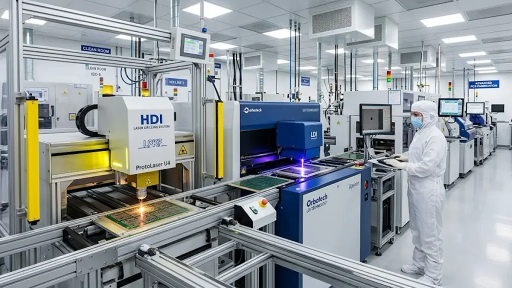
Advanced HDI Laser Drilling and LDI Manufacturing Line for Embedded Passive PCBs
Modern embedded passive designs increasingly overlap with advanced HDI manufacturing.
Laser drilling can create microvias that connect internal structures without consuming the same amount of board area as larger conventional vias.
For complex designs, the combination of:
Embedded Passives + HDI + Microvias + Fine-Line Routing
can provide significantly greater routing flexibility.
Laser processing also becomes important when the design requires very small interconnection geometries.
For a supplier evaluation, procurement teams should look beyond the equipment name and ask for the manufacturer’s qualified production capability for the relevant structure.
The important questions are:
- What microvia dimensions are routinely manufactured?
- What registration capability is achieved in production?
- Which materials can be processed?
- Can the process support prototypes and volume production?
- How is microvia quality verified?
Equipment capability is valuable only when it translates into repeatable production performance.
How Do LDI and Fine-Line PCB Technology Influence Embedded Passive PCB Design?
Laser Direct Imaging can support increasingly dense PCB geometries by improving imaging precision and reducing some limitations associated with conventional phototools.
For embedded passive structures, this can become important when:
- Passive structures occupy small areas
- Microvias must connect to fine pads
- Multiple internal functions are densely arranged
- Routing channels are limited
- Registration windows become narrow
Fine-line and mSAP technologies can further expand the available routing density for advanced PCB structures.
This means the evolution of embedded passive PCB technology is closely connected with the development of HDI, mSAP, laser processing and high-precision registration.
What Reliability Issues Should Be Considered for Embedded Passive PCBs?
Reliability is one of the areas where embedded passive technology requires a different engineering mindset.
Thermal Expansion
The PCB and embedded materials may have different coefficients of thermal expansion.
Repeated temperature changes can create mechanical stress at interfaces.
Lamination Stress
Embedded structures are subjected to thermal and mechanical conditions during multilayer fabrication.
The compatibility of the component, dielectric and copper structure must therefore be evaluated.
Electrical Stability
For embedded resistors, resistance drift can be influenced by:
- Temperature
- Material stability
- Humidity
- Process variation
- Long-term operating conditions
For embedded capacitors, capacitance and dielectric behavior must be evaluated against the intended operating environment.
Interconnection Reliability
Microvias and internal connections should be evaluated for their ability to withstand thermal and mechanical cycling.
For demanding applications, reliability validation should be based on the actual stack-up and operating environment rather than generic PCB data.
How Should Embedded Passive PCB Designs Be Tested?
Testing should reflect the function of the embedded structure.
Electrical Testing
Electrical testing can verify:
- Continuity
- Isolation
- Resistance
- Selected capacitance characteristics
- Interconnection integrity
Cross-Section Analysis
Cross-sections can reveal:
- Layer registration
- Dielectric thickness
- Via structure
- Copper thickness
- Component placement
- Lamination quality
X-Ray Inspection
X-ray can be particularly useful when critical structures are hidden inside the PCB and cannot be visually inspected from the surface.
Thermal and Reliability Evaluation
For demanding applications, testing may include thermal cycling and other environmental reliability evaluations appropriate to the product.
The objective is not simply to prove that the board works immediately after production.
The objective is to establish confidence that the embedded structure remains within specification throughout its intended operating life.
When Should Engineers Choose Embedded Passive Components?
Embedded passive technology is most attractive when at least one of the following conditions exists:
The PCB Surface Is Crowded
If the surface has insufficient space for additional passive components, internal integration can create valuable design capacity.
The Electrical Path Must Be Minimized
Applications sensitive to interconnection parasitics may benefit from integrating the passive function closer to the circuit.
Component Count Is High
Large numbers of small passive components can consume significant assembly area.
Product Thickness Is Restricted
Moving selected functions inside the PCB can help designers work within a constrained mechanical envelope.
Assembly Complexity Needs to Be Reduced
Embedding selected passive functions can eliminate some surface-mount placement and soldering operations.
However, embedding should not be selected automatically.
If a component requires frequent tuning, field replacement or easy debugging, conventional surface mounting may still be the better engineering decision.
When Should You Avoid Embedded Passive Components?
There are situations where conventional SMT remains more appropriate.
Avoid unnecessary embedding when:
- The board has sufficient surface area.
- Components require frequent replacement.
- Design parameters are likely to change during development.
- The embedded structure provides little system-level benefit.
- Production volume does not justify the additional engineering effort.
- The component requires easy visual inspection.
- The manufacturing process cannot maintain the required tolerance.
The correct question is therefore not:
“Is embedded technology more advanced?”
It is:
“Does embedding create enough technical or commercial value to justify its manufacturing complexity?”
How Much Does an Embedded Passive PCB Cost?
There is no universal price for an Embedded Passive PCB because cost depends on the complete structure.
Major variables include:
- PCB dimensions
- Layer count
- Material system
- Embedded passive type
- Resistance/capacitance tolerance
- Cavity requirements
- Microvia density
- Fine-line requirements
- Lamination sequence
- Inspection requirements
- Prototype quantity
- Production volume
- Yield
A useful procurement model is:
Total Cost = PCB Fabrication + Embedded Component Processing + Tooling + Inspection + Testing + Yield Impact + Engineering Cost
This is more useful than comparing only the quoted PCB unit price.
For high-volume programs, a slightly higher fabrication price may be justified if embedded passives significantly reduce surface assembly operations.
How Should Buyers Evaluate an Embedded Passive PCB Manufacturer?
Selecting an Embedded Passive PCB Manufacturer requires more than checking whether the supplier lists “embedded PCB” on its website.
Procurement teams should verify five areas.
1. Material Capability
Ask whether the supplier has experience with:
- Resistive materials
- Embedded capacitor structures
- High-Tg materials
- Low-loss materials
- Specialized dielectric systems
2. Process Capability
Verify experience with:
- Multilayer lamination
- Sequential build-up
- Laser microvias
- Fine-line routing
- Copper filling
- Internal registration
3. Inspection Capability
Ask how hidden structures are verified.
Relevant capabilities may include:
- AOI
- X-ray
- Cross-section analysis
- Electrical testing
- Dimensional inspection
4. Engineering Support
A capable supplier should be able to review:
- Component dimensions
- Stack-up
- Material compatibility
- Clearance
- Via structures
- Tolerance
- Manufacturing yield
5. Prototype-to-Production Transfer
The supplier should demonstrate that the embedded passive process can be stabilized beyond prototype production.
This is particularly important for customers developing automotive, medical, industrial or other reliability-sensitive products.
What Should Be Included in an Embedded Passive Components PCB RFQ?
A high-quality RFQ should give the manufacturer enough information to assess both electrical and manufacturing feasibility.
Recommended information includes:
PCB Information
- Board dimensions
- Layer count
- Finished thickness
- Copper thickness
- Stack-up
Embedded Passive Information
- Component type
- Resistance or capacitance value
- Tolerance
- Component dimensions
- Location
- Required operating temperature
- Electrical specifications
Manufacturing Information
- Via structure
- Microvia requirements
- Surface finish
- Material requirements
- Impedance requirements
- Inspection requirements
Commercial Information
- Prototype quantity
- Production quantity
- Annual demand
- Target lead time
- Packaging requirements
Providing this information early allows the manufacturer to identify potential DFM issues before the quotation becomes a production commitment.
What Are the Most Common Embedded Passive PCB Design Mistakes?
Treating an Embedded Passive as a Normal SMT Component
An embedded structure interacts with the PCB stack-up and lamination process.
It cannot always be transferred directly from an SMT design.
Ignoring Material Tolerance
The nominal electrical value is only one part of the specification.
Material tolerance and process variation also affect the final result.
Designing the Component Before the Stack-Up
Embedded passive geometry should be developed together with the stack-up.
Leaving DFM Until After the RFQ
Late DFM review can force changes to:
- Component dimensions
- Layer thickness
- Via positions
- Material selection
- Clearance
Optimizing Unit Price Instead of Total Cost
The cheapest quotation may not provide the lowest overall project cost if yield, testing and assembly savings are ignored.
How Is Embedded Passive PCB Technology Evolving in 2026?
The development of embedded passive technology is increasingly connected to several broader PCB manufacturing trends.
Higher-Density HDI
As electronic packages become smaller, embedded passives are increasingly being combined with high-density interconnect structures.
Fine-Line and mSAP Processing
More precise circuit formation creates additional freedom for integrating small passive structures into dense PCB architectures.
Advanced Laser Processing
Smaller and more accurately positioned microvias enable higher interconnection density around embedded structures.
More Sophisticated Inspection
As more critical functions move inside the PCB, X-ray, cross-section analysis and electrical validation become increasingly important.
PCB and Packaging Convergence
The boundary between advanced PCB fabrication and electronic packaging continues to become less distinct.
Embedded passive structures are part of this broader movement toward three-dimensional electronic integration.
For manufacturers, this means equipment capability alone is no longer enough. Process integration and repeatability increasingly determine whether advanced embedded passive designs can be manufactured economically.
How Can Shenzhen Hongda Circuit Technology Support Embedded Passive PCB Projects?
For customers developing Embedded Passive Components PCB, Shenzhen Hongda Circuit Technology Co., Ltd. can approach the project from both the PCB fabrication and advanced process-control perspective.
The company’s manufacturing portfolio includes technologies relevant to high-density embedded structures, including:
- LDI imaging
- Laser drilling
- HDI microvias
- Fine-line PCB processing
- mSAP-related manufacturing
- Automated plating
- AOI inspection
- X-ray inspection
- Multilayer PCB fabrication
These capabilities are important because embedded passive PCB production requires multiple processes to remain aligned.
For example, a design may require a passive structure to be positioned accurately within the stack-up, followed by controlled lamination, microvia formation, fine-line circuit fabrication and inspection.
The practical manufacturing objective is therefore:
Design feasibility → Process compatibility → Stable fabrication → Inspection → Electrical validation → Repeatable production
For procurement teams, this integrated approach can reduce the risk of qualifying a supplier that can produce a prototype but struggles to maintain consistent volume production.
Shenzhen Hongda Circuit Technology Co., Ltd.
Website: www.pcbkr.com Email: pcb@pcbkr.com
Embedded Passive PCB Procurement Checklist
Before approving an Embedded Passive PCB Manufacturer, procurement teams can use the following checklist:
| Evaluation Area | Questions to Ask |
|---|---|
| Passive technology | What types of embedded passives can you manufacture? |
| Resistors | What resistance range and tolerance can be controlled? |
| Capacitors | What dielectric and capacitance structures are available? |
| Materials | Can you process the required dielectric and resistive materials? |
| Stack-up | Can your engineering team review the embedded stack-up? |
| Laser | What microvia technology is available? |
| Fine-line | What production line/space capability is qualified? |
| Lamination | How are internal structures controlled during lamination? |
| Inspection | How are hidden defects detected? |
| Reliability | What validation can be performed? |
| Prototype | Can prototypes be produced before volume production? |
| Yield | What is the expected production yield? |
| Engineering | Is DFM support available before PO release? |
| Volume | Can the process be transferred from prototype to mass production? |
Frequently Asked Questions About Embedded Passive Components
What are embedded passive components in PCB?
Embedded passive components are resistor, capacitor, inductor or other passive functions integrated into the internal PCB structure rather than mounted exclusively on the board surface.
Can resistors and capacitors be embedded in a PCB?
Yes. Embedded resistors and capacitors are among the principal applications of embedded passive PCB technology. They can be implemented through discrete internal components or specially engineered PCB materials and structures.
Are embedded passive PCBs better than conventional SMT PCBs?
Not universally. Embedded passives can provide advantages in space utilization, integration density and selected electrical applications, but conventional SMT remains preferable when easy replacement, tuning, inspection or low manufacturing complexity is more important.
Are embedded passive PCBs more expensive?
The PCB fabrication process can be more complex and therefore may have a higher initial manufacturing cost. However, the total economic benefit can improve when embedding reduces assembly operations, surface area or system size.
How do I choose an embedded passive PCB manufacturer?
Evaluate the supplier’s material capability, embedded-process experience, lamination control, laser microvia technology, fine-line capability, inspection systems, reliability testing, DFM support, prototype capability and production yield—not only the quoted unit price.
When Does Embedded Passive PCB Technology Make Commercial Sense?
Embedded Passive Components become valuable when the PCB itself needs to perform more of the electrical work while using less external component space.
The technology can provide an effective solution for designs where:
- PCB area is limited
- Component density is high
- Electrical paths need to be compact
- Power integrity is important
- Product thickness is constrained
- Assembly complexity must be reduced
But successful implementation requires more than selecting an embedded resistor or capacitor.
The complete solution depends on the interaction between:
Passive Component Technology + PCB Materials + Stack-Up + Lamination + Microvias + Fine-Line Circuits + Inspection + Reliability
For engineering and procurement teams, the most important decision is therefore to select a manufacturing partner early enough to evaluate the complete structure.
A capable Embedded Passive PCB Manufacturer should not simply quote the drawing. The supplier should help determine whether the proposed embedded structure can be manufactured consistently, inspected effectively and scaled from prototype to production.
That is where advanced PCB engineering turns embedded passive technology from a design concept into a manufacturable product.
Shenzhen Hongda Circuit Technology Co., Ltd.
Email: pcb@pcbkr.com Website: www.pcbkr.com
About Author
David Chen https://www.linkedin.com/in/pcbcoming
David Chen boasts an extensive professional background in PCBA manufacturing, PCBA testing, and PCBA optimization, with specialized expertise in high-precision PCBA fault analysis and rigorous PCBA reliability testing. The author has worked with high-layer-count server PCB fabrication, ultra-low-loss backplane stackups, and thermo-mechanical reliability optimization for AI infrastructure projects involving 112G and 224G PAM4 architectures. Skilled in complex circuit design and cutting-edge advanced PCB manufacturing processes, he delivers solutions that elevate product durability and performance across industrial applications. His technical articles focusing on PCBA manufacturing workflows and testing methodologies are widely cited by industry peers, research institutions, and technical platforms, solidifying his reputation as a recognized technical authority in the global circuit board manufacturing sector.